MILLENNJUM INFORMATION SYSTEMS ,INC.
UNIVERSAL ONE
Microco~er
Development System
UNIVERSAL ONE
Microcom:pJlter
Development System
Hardware Reference
Manual
TABLE OF CONTENTS
Chapter 1 INTRODUCTION
1.0 1.1 1.2 1.3 1.4 1.5 1.6
Universal One System Computer Components . . Development Software
Universal Emulator . . . Universal Emulator Software. Purpose of this Manual
Manual Contents . . . . . .
Chapter 2 DEVELOPMENT COMPUTER DESCRIPTION
2.0 2.1 2.2 2.3 2.4 2.5 2.5.1 2.5.2 2.5.3 2.5.4 2.5.5 2.5.6 2.5.7 2.5.8 2.5.9 2.5.10 2.5.11 Chapter 3.0 3.1 3.1.1 3.1. 2 3.1.2 3.1.4 3.2 3.2.1 3.2.2 3.2.3 3.2.4 3.2.5 3.3 3.3.1 3.3.2 3.3.3
Computer Architecture Memory Organization . . Bus Structure . . . . Debug Hardware
I/O Provisions
Development Computer Subassemblies Master CPU Module . . . . Slave CPU and Emulation Interface Debug and Front Panel I/O Module Master Memory . . . . .
Slave Memory . . . .
4K RAM/2K PROM Module . . . . 16K Dynamic RAM Module
General Purpose I/O Module PROM Programmer Modules . . Hardware Analyzer Module Emulation Cable . . . .
3 MASTER CPU MODULE
Introduction
General Description
The CPU . . . .
I/O Logic
Interrupt Logic . . DMA Logic . . . .
Detailed Description . . . . 2650 CPU Support
I/O Logic . . .
Interrupt Logic . . .
DMA Logic . . . .
Baud Rate and Timer Logic
Utilization . . . .
Installation . . . . Switch and Jumper Options
Interface and Connector Pinouts .
TABLE OF CONTENTS (Continued)
Chapter 4 DEBUG AND FRONT PANEL I/O MODULE Page
4.0 Introduction
·
·
· ·
4-14.1 General Description
·
4-14.1.1 Master/Slave Control 4-2
4.1.2 Debug Features
·
· . ·
· . ·
4-24.1.3 I/O Commands and In.terrupts 4-6
4.1.4 Front Panel Interface 4-6
4.2 Detailed Description
·
4-84.2.1 Master/Slave Control and Halt Detector 4-8
4.2.2 I/O Commands and Interrupts
·
·
4-104.2.3 Debug Features 4-17
4.2.4 Front Panel Interface
·
4-214.3 Utilization
·
·
· .
4-234.3.1 Installation 4-23
4.3.2 Switch and Jumper Options
· .
4-254.3.3 Interface and Connector Pinouts '.
·
4-25Chapter 5 RAM/PROM MEMORY MODULE Page
5.0 General Description
·
·
5-15.1 Detailed Description
·
5-15. 1.1 Memory El ements
.
·
·
5-15.1.2 PROM Addressing 5-2
5.1.3 RAM Address i ng
·
·
5-25.1.4 Timing
. .
5-25.1.5 -9V Regulator
·
·
· ·
5-45.2 Utilization 5-4
5.2.1 Installation
·
5-45.2.2 Switch and Jumper Options 5-5
5.2.3 Interface and Connector Pinouts
·
5-7Chapter 6 16K DYNAMIC RAM MODULE Page
6.0 Introduction 6-1
6.1 General Description
·
·
6-16.2 Detailed Description
.
·
·
6-66.2.1 RAM Storage 6-6
6.2.2 PROM Memory
· ·
.
·
6-66.2.3 Module Select and System Request Logic 6-8
6.2.4 Byte/Word Control
·
· ·
6-106.2.5 Address Control
·
6-106.2.6 Data-Parity Control
·
·
6-146.2.7 Refresh Request Logic
·
·
6-166.2.8 Operation Control and Timing
·
6-196.3 Utilization
. . ·
. ·
6-206.3.1 Installation
·
·
·
·
·
6-206.3.2 Switch and Jumper Options
· ·
6-22TABLE OF CONTENTS (Continued)
Chapter 7 GENERAL PURPOSE I/O MODULE
7.0 7.1 7.2 7.2.1 7.2.2 7.2.3 7.2.4 7.3 7.3.1 7.3.2 7.3.3
Introduction . . . . . General Description Detailed Description .
Serial I/O Ports .
Module and Port Address Control Parallel Input and Output Ports Interrupt Logic . . . .
Utilization . . . . Installation . . . . Switch and Jumper Options . . . .
Interface and Connector Pinouts . . . .
Chapter 8 1702A AND 82S115 PROM PROGRAMMER MODULES
8.0 8.1 8.2 8.2.1 8.2.2 8.2.3 8.2.4 8.3 8.3.1 8.3.2 8.3.3 8.3.4 8.4 8.4.1 8.4.2 8.4.3 8.5 8.5.1 8.5.2 8.5.3.
Introduction . . . . General Description . . . .
1702A Detailed Description Operation . . . . Data Control . . . . Power Supplies . . . . Sequencer and Voltage Switches. 82S115 Detailed Description
Operation . . . . Data Control . . . .
Power Supplies . . . . Sequencer and Voltage Switches . .
Utilization: 1702A . . . .
Installation . . . . Switch and Jumper Options . . .
Interface and Connector Pinouts . . Utilization . . . .
Installation . . . . Switch and Jumper Options
Interface and Connector Pinouts
Chapter 9 SYSTEM BUS
9.0 9.1 9.2
General Description . Bus Signal Definitions . Motherboard Pin Lists
TABLE OF CONTENTS (Continued)
Chapter 10 FRONT PANEL Page
10.0 Introduction
.
·
10-110.1 Functional Description
·
·
10-110.1. 1 Address, Data Entry and Display
·
·
10-310.1.2 System '.
.
10-410.1.3 CPU Control Swtiches
. .
10-410.1.4 Bus Control Switches
·
·
10-510.1. 5 Bus Status I n d i ca to rs .
·
10-610.1.6 CPU Status Indicators.
.
10-610.1.7 System Status Indicators
.
·
10-610.1.8 PROM Programming Sockets and Power Switches 10-6
10.2 Theory of Operation
·
10-710.2.1 Data and Address Logic 10-10
10.2.2 Bus Access Logic
·
10-1210.2.3 CPU Control Logic
.
10-13Chapter 1
INTRODUCTION
1.0 UNIVERSAL ONE SYSTEM
The Universal One development system is a complete general purpose tool, supporting in turn - key fashion all phases of user software and hardware
development. Its basic structure and capability is similar to a general
purpose minicomputer system but with two very important added features. It provides multiple in-circuit emulation capability for exercising and debugging user programs and prototype systems and it contains both bipolar and MOS PROM programming capability integral to the system.
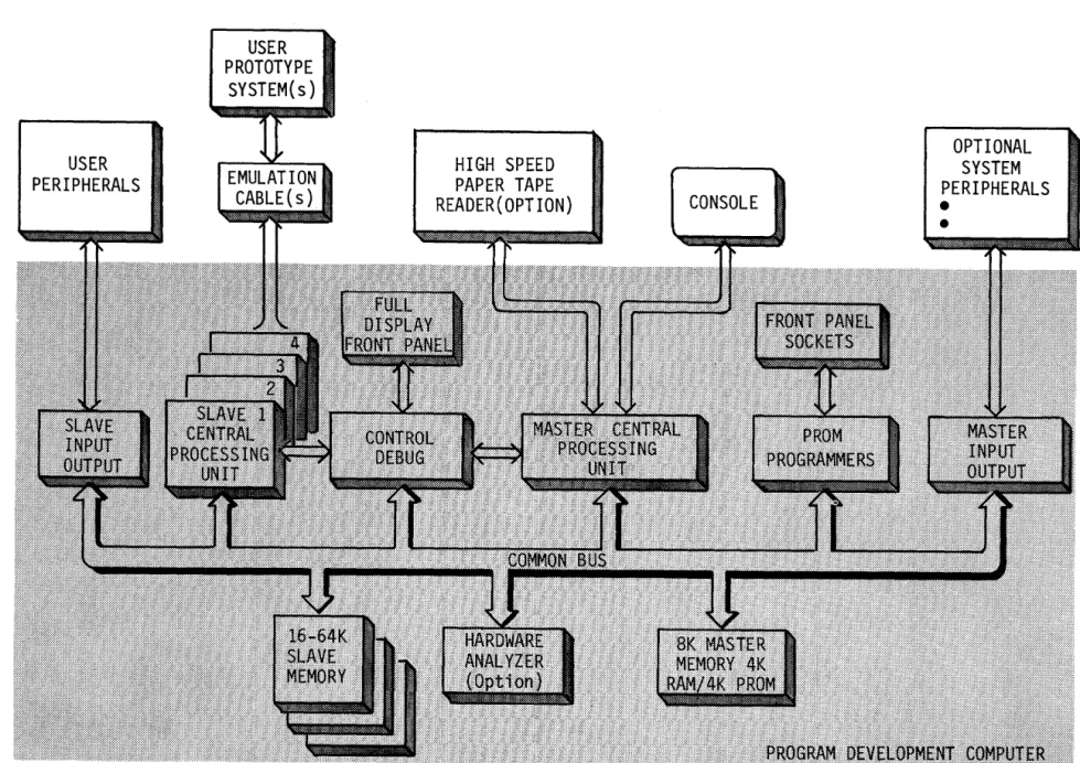
The system components, illustrated in figure 1-1 consist of the Development Computer, the Dual Floppy Disk unit, the Console (CRT or TTY) and one or more Emulation cables. Emphasis has been placed on universality and ease of opera-tion. Due to its Master-Slave structure new microprocessors can be supported with the addition of a single printed circuit module. Basic software and hardware remains unchanged. Thus, the system becomes more valuable with time, supporting more processors rather than becoming obsolete as tech-nology advances.
Ease of operation is insured through use of an interrupt driven floppy disk based operating system. The software features include:
Floppy Disk Operating System Comprehensive system monitor Disk file manager
Text edi tor
Comprehensive Debug Software Breakpoint detection Program tracing Program stepping
Static state processor control
Comprehensive Diagnostic Package System peripherals
Memory diagnostics CPU diagnostics System diagnostics
The dual expandable Disk System is controlled by its own internal micro-processor relieving the computer system of time consuming hardware re-lated functions and error checking.
In-Circuit Emulation to debug the user protot~pe is as easy as unplugging
the microprocessor chip in the user breadboard and plugging the Emulation Cable into its socket. Full debug capability with system RAM and user I/O or user memory and I/O is supported. The cable actually operates with the real microprocessor, not a simulation, allowing the user to isolate tim-ing and interface problems related to the processor as well as his peri-pheral devices.
1.1 COMPUTER COMPONENTS
The Development Computer is completely modular with a bus oriented struc-ture. The Computer contains the following components:
- MASTER CENTRAL PROCESSING UNIT, based on the 2650, which
su-pervises the overall system and contains the basic system I/O interface (Console and Disk Subsystems).
- PROTECTED 16K BYTE MASTER MEMORY containing the system
soft-ware.
- SLAVE PROCESSING UNITS, containing 8 or 16 bit
t-A
I
W
USER PERIPHERALS
/
USER PROTOTYPE
SYSTEM(s)
EMULATION CABLE(s)
DUAL DISK STORAGE SUBSYSTEM
DISl1:t: , , - - -
~--~DRIVE
EXPANSION DRIVEINTELLEGENT CONTROLLER
PRINTER
CONSOLE
FIGURE 1-1 THE UNIVERSAL ONE SYSTEM
OPTIONAL SYSTEM PERIPHERALS
- 16K BYTE/WORD SLAVE RAM MEMORY expandable to 64K byte for user programs. Any mixture of RAM and ROM may be used.
- EMULATION CABLE(s) which replace user microprocessor with Slave processor to allow full debugging of user hardware.
- DEBUG MODULE which supports software debug features such as TRACE, BREAKPOINT and GO. It also interfaces both front panels.
- HARDWARE ANALYZER (option) Provides expanded breakpoints, 128 transaction real time trace storage and User memory mapping.
- GENERAL PURPOSE I/O MODULE (option) Contains RS-232 serial interface and custom configurable parallel 8 bit ports. It may be used for additional system peripherals such as a Modem or High Speed Paper Tape Reader, or for user peripherals.
- PROM PROGRAMMERS (optipn) Three front panel sockets and two independent programming modules provide erasable MOS PROM and bipolar PROM programming capability.
The unit physically consists of a 20 slot card file for 11" x ]I' circuit modules, a snap on front panel, a power supply module containing reserve power for custom user cards, and a dual fan system for reliable cooling. The unit is extremely modular for ease of replacement of any component.
The card file contains a universal bus structure to all positions except that the bus is split into Master-Slave halves with control and interrupt lines unique to each half. Master and Slave proces,sors and their memory and I/O maybe placed anywhere within their designated halves. The mother-board contains an auxiliary power bus for special user voltage requirements and it contains a 16 bit data bus to accommodate 16 bit Slave processors and memory.
contains hexadec1r,l1al data and addresses displays, paddle handle address and data entry switches, memory and I/O examine and alter functions, as well as single step and system control functions. Back lit displays in-dicate system states.
1.2 DEVELOPMENT SOFTWARE
System software provided with the Prototype Development System includes the Millennium Universal Disk Operating System (UDOS) and the Text Edi-tor. The Assembler and the Debug software are provided with each Slave supported by the system.
UDOS -- UDOS relieves the user of the necessity of understanding detailed
internal operation of the system. It provides complete control over
opera-tion of all poropera-tions of the Prototype Development System. All funcopera-tions relating to file handling, loading and execution are monitored and control-led by UDOS, including in-circuit emulation and PROM programming functions. UDOS resides in a dedicated memory consisting of 256 byte PROM and 16K RAM running under the Master CPU.
The UDOS software allows the user to create, edit, and assemble files; obtain object and listing outputs; load and execute programs; and, through the debug system, check out programs in an efficient manner.
UDOS provides a powerful command file capability that enables the user to create customized operating system commands.
UDOS controls the multi-drive Floppy Disk Subsystem, a Line Printer, and the CRT Console, which may be an ASR-33 TTY or an RS-232 compatible device. Software drivers are provided within UDOS for these I/O devices. The UDOS software provides a flexible input/output system that enables the user to dynamically assign any logical channel to any physical device or file within the system. In this way, system I/O devices may be dynamically assigned
using UDOS commands either from the console or from within a user's program. Thus, the user may write his own driver for other peripheral devices and
link them into the UDOS system by use of the optional General Purpose I/O Card.
TEXT EDITOR -- The Text Editor is a comprehensive software package that
allows the user to enter and modify text files. The Text Editor is line oriented and accepts inputs from the terminal or a disk file, performs modifications in a work space, and outputs the revised text to a disk file.
ASSEMBLER -- The Prototype Development System Resident Assembler
trans-lates symbolic assembly language instructions into appropriate machine language code.
The Assembler generates absolute object code. This code is in hexadecimal format and may be loaded into the system for direct execution or may be converted by an UDOS command to SMS format for PROM or ROM programming.
DEBUG -- The Debug system is a software program which provides the user
with real-time program debug capabilities within both a software and
hard-ware environment. It uses special hardware features built into the program
development system to control execution of the user's program. User
pro-grams operating under the Debug system have dynamic program trace, break-point capabilities, and memory modification capabilities. Status reporting on the memory, the program, and the processor is also provided.
1.3 UNIVERSAL EMULATOR
USER
PERIPHERALS
USER
PROTOTYPE
SYSTEM(s)
EMULATION
CABLE(s)
HIGH SPEED
PAPER TAPE
READER(OPTION)
CONSOLE
FIGURE 1-2 THE UNIVERSAL EMULATOR SYSTEM
OPTIONAL
SYSTEM
PERIPHERALS
•
additional capability to be loaded in the 4K of Master RAM Memory. The basic configuration consists of the Master CPU, 4K PROM Master Memory, 4K of RAM Master Memory, the Debug card, 4K of Slave Memory and a Slave CPU with the Emulation Cable. The Universal Emulator is also
supplied with extended front pan~l capability.
1.4 UNIVERSAL EMULATOR SOFTWARE
The Universal Emulator software is broken down into three functional areas. Software features which are independent of the Slave processor are
contained in the Master PROM memory. Software features which are optional
and/or dependent on the Slave processor can either be loaded into Master RAM from the TTY or contained on PROM housed on the particular Slave CPU card.
1.5 PURPOSE OF THIS MANUAL
This manual is intended to acquaint an experienced logic designer with the Millennium Universal Microprocessor Development Systems, both in over-all concept and architecture, and in detail. The descriptions of functions and the detailed descriptions of each module in the system should be suf-ficient to allow troubleshooting to the board level in case of failure. It is assumed that the reader has some knowledge of microcomputer develop-ment systems and knowledge of the characteristics of the Slave micropro-cessor being used in the product. For a detailed description of system
operation refer to the Universal One or Universal Emulator Operator's Manual.
1.6 MANUAL CONTENTS
peripherals are mentioned briefly in Chapter 2, but detailed descriptions and operating theory are not provided. The reader is referred to the manuals for each peripheral deyice for operating and maintenance.
Chapter 2
DEVELOPMENT COMPUTER DESCRIPTION
2.0 COMPUTER ARCHITECTURE
The Development Computer is based on a dual processor concept, as shown in figure 2-1. The Master CPU runs the Operating System and the Text Editor and performs all interactions with system I/O devices. The Slave CPU runs user programs as well as the Assembler. The Master CPU has completely separate memory and I/O, protected from user programs. This provides a crashproof Operating System and gives the user total use of the Slave Memory and I/O address space.*
The dual processor architecture permits different Slave CPU's to be sup-ported by the system without requiring a re-write of the Operating System software. Only those portions of the system software unique to the Slave CPU being supported (the Assembler and portions of the Debugger) must be updated. Hardware provisions within the computer permit support of S1ave CPU's of up-to 16-bit word length and up to 64K address space.
Interaction of Master and Slave CPU's is controlled by the Debug module under Master CPU direction. Both CPU's share the basic bus structure, with only one processor active at anyone time. Control is transferred to the Slave by a Master HALT. Control is returned to the Master by any system interrupt or a Debug interrupt such as a breakpoint.
The bus structure is essentially universal for all board locations in the card file, with minor exceptions. The Debug board splits the bus
* For the Slave CPU a 100 -lK byte segment of Slave Memory is required for Master/Slave interface when running the Slave CPU under Debug control. For the 8080, this is provided by a 1K PROM at the upper memory boundary. '
into Master and Slave halves, with a separate interrupt structure for each ha 1 f. The PROM Programmer boards' have dedi cated 1 ocati ons because of the special AC voltages required for programmer operation. Memory or I/O boards may be placed in any open position in the appropriate half of the card file.
The Emulator Cable assembly provides in-circuit emulation of user hard-ware. The cable connects to the Slave CPU on one end and essentially replaces the CPU in user hardwa.re on the other end. This gives total debugging capability in an actual hardware environment.
The Master CPU contains provision for the basic system I/O which consists of the Floppy Disk and Printer interface and the system Console interface. General Purpose I/O modules can provide a full ElA· RS-232-C interface and parallel I/O ports to interface additional system peripherals.
With UDOS, the Slave CPU can utilize the system peripherals through Ser-vice Calls (SVC·s) to the operating system. SVC·s are described in Chap-ter 9 of the Operator·s Manual. Also special user peripherals 'under direct
Slave control may b'ei nterfaced with the use of a General Purpose I/O module.
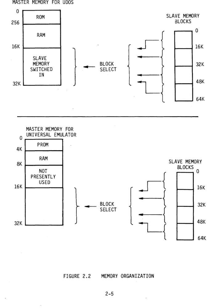
2.1 MEMORY ORGANIZATION
For UDOS, Master Memory consist of 16K of RAM, with the first 256 bytes overridden by PROM which contains the system bootstrap program. When the system is initialized, the Master accesses the bootstrap to load the operat-ing system from the system diskette into Master Memory. For the Universal Emulator, Master Memory consists of 4K PROM and 4K RAM.
Slave Memory contains 16K bytes of RAM in the UDOS system and 4K bytes in the Emulator system, both expandable to 64K bytes. The Slave has ac-cess to Slave Memory only, while the Master has acac-cess to both memories. A 16K byte portion of Slave Memory is assigned under program control to
N
I
W
USER PERIPHERALS
USER PROTOTYPE TEST J.I PROCESSOR
CLIPS SOCKET·
BUFFER EMULATION CABLE
CONSOLE (CRT OR
TTY)
FLOPPY DISK STORAGE SUBSYSTEM
the Master's 16K-32K address space as illustrated in figure 2-2. The ability of the Master to "bank switch" Slave Memory into its address space allows communication for I/O Service Calls, Debug Trace operation, and Text Editor operation.
2.2 BUS STRUCTURE
The Computer bus structure is shown in figure 2-3. The bus is split into Master and Slave sections by the Debug and front panel I/O Logic board. The bus is essentially universal in that data, address, and control lines are paralelled to all boards. The exceptions ,to this structure are the independent Debug control and interrupt lines for the Master and Slave,
an~ special PROM AC power lines. The bus structure allows freedom of Memory, CPU and I/O module placement within each half of the bus. I/O and Memory address assignment is switch selected on the individual boards.
The bus consists of 100 lines made up of the following signals:
COMMON BUS LINES
16 Address lines 16 Data lines 22 Control lines:
9 Memory and I/O Control lines 8 System Control
lines
3 Debug lines 2 Sense/Flag lines 2 Interrupt
20 Power and Ground lines 3 Spare
UNIQUE LINES
SLAVE HALF 6 Debug 1 i nes
13 Interrupt-related lines 2 Spare 1 i nes
MASTER HALF 4 Debug lines
17 Interrupt-related lines
PROM PROGRAMMER SECTION 14 AC Voltage lines
Four of the 20 power and ground pins provide an auxiliary power bus which can be connected via rear-panel terminals to an external power supply for
MASTER MEMORY FOR UDOS
o
ROM SLAVE MEMORY
256 BLOCKS
16K
RAM
..s-{
0
16K
SLAVE
...
MEMORY
SWITCHED
----
BLOCK SELECT 32KIN ~
L{
48K 64K 32KMASTER MEMORY FOR
0 UNIVERSAL EMULATOR
PROM 4K
RAM
SLAVE MEMORY 8K
BLOCKS NOT
F{
0
PRESENTLY USED
16K 16K
4 {
~ BLOCK 32K
SELECT
~
{
32K 48K
'-{
64Kuser requirements not met by the standard system supplies. The AC voltages required by the PROM programmers extend to the end board positions only and mechanical keying prevents pJugging any other boards into those posi-tions. All board connectors are offset to prevent plugging boards in backwards.
A complete description of all bus signals is contained in cbapter9.·
2.3 DEBUG HARDWARE
Hardware is contained on both the Debug module and Slave CPU module to facilitate the following major system Debug features:
- Master/Slave interaction
Breakpoints
Forced Slave Jumps
Master/Slave Interaction -- All Debug hardware communication to the
Master CPU is by way of interrupts. The Master reliquishes control to the Slave CPU by performing a HALT instruction. Control is regained by the Master when it receives an interrupt. Interrupts may be from.system I/O or from the Debug hardware. The Debug module contains its own inter-rupt priority decoder and vector generator for Debug and Service call interrupts.
Breakpoints -- Two breakpoint registers are contained on the Debug module.
The breakpoint addresses are loaded by the Master CPU under command from the user. When a breakpoint address is identical to the current Slave CPU address, the Master CPU is interrupted before the next Slave
instruc-tion fetch. Both the IIlastll instruction address and the IInextll
instruction address are stored. This allows the software to examine the Slave's pro-gram and interpret op-codes for the trace printout. It also allows the system to restore the Slave to its original address after executing a
N
I ...
DC POWER
AC POWER
PROM MASTER SLAVE
PROGRAMMERS SECTION DEBUG MODULE SECTION
,,.-_----J~_---,.,
.,.-_ _ _ _
--'A _ _ _ _ _ _ _ \ r---A"---~\•
~
• I I I •
I • I
POWER AND GROUND
CONTROL
ADDRESS
DATA
MASTER INTERRUPT SLAVE INTERRUPT
MASTER DEBUG SLAVE DEBUG
m.J
W 11
II
-
_
~ ~m
~ ~ ~W _ _
register dump routine.
Forced Slave Jumps -- Forced Slave Jumps are required for three reasons:
1) To start execution of the user's program at any commanded
location.
2) To allow Slave execution of register dump and register restore routines for trace.
3) To allow Slave execution of commands relating to user memory modification.
The jump address is cont~ined in a register in the Debug module and the
Forced Jump logic is contained on the Slave CPU module.
Emulation Cable -- The Emulation Cable allows the user to exercise his
hardware while still retaining the Debug features of the deve1bpment system. The cable connects to the Slave CPU on one end and plugs into the user's prototype microprocessor socket on the other. The cable con-tains line drivers and receivers close to the user end to insure signal integrity and minimize user circuit loading.
The Slave CPU essentially acts as the user's microprocessor. There are two basic in-circuit modes of operation illustrated in figure 2-4a, band
c. In Mode 1, the user's I/O is exercised while the program is executing
out of the computer Slave Memory. Full Debug and trace operations are
available. In Mode 2, both the user's I/O and memory are utilized, still allowing breakpoints, single step, and trace. Multiplexers on the Slave board switch between the cable interface and the computer bus for each
mode. The cable can remain installed in the normal Slave CPU mode with
no adverse effects. An optional Hardware Analyzer Module allows mapping Sl ave Memory in 256 byte blocks to ei ther the user', prototype system or the computer system while in Emulation mode 1.
A
IN-COMPUTER EXECUTION SYSTEMI/O DEVICES
~
~
MASTER SLAVE
-,
"
,
I'I
;
,",v
'"
MEMORY MEMORY
>;yti,tWt1%BfumM&1;\'<to,".{
B
EMULATION CABLE MODE 1MASTER SLAVE
MEMORY MEMORY
C
EMULATION CABLE MODE 2MASTER SLAVE
MEMORY
I.,
"-GP I/O
... ,
EMULATION CABLE
EMULATION CABLE
USER I/O
USER PROTOTYPE
I/O
USER PROTOTYPE
MEMORY AND
2.4 1/0 PROVISIONS
The basic computer I/O consists of the Floppy Disk and Console interface as shown in figure 2-1. These are both contained on the Master CPU. The Floppy Disk interface uses 8 bit parallel input and output ports for data and control. A 40 pin ribbon cable on the top edge of the Mas ter connects di rectly to the Floppy Di sk Sys tern.
The console (normally CRT or TTY) is a serial interface providing a limited EIA RS-232-C interface and a 20 ma TTY current loop interface. Baud rates and data formats are switch selectable for TTY or EIA opera-tion. Additional switch P9sitions select the EIA Baud rate for 150-2400. A 25 pin standard EIA connector on the rear panel connects through a ribbon cable to the top edge of the Master CPU board.
The General Purpose I/O board allows both system I/O expansion and user in computer I/O capability. The board contains a full RS-232-C interface, four sets of 8 bit parallel I/O ports, and eight interrupt flip-flops. This allows a hardware interface to most TTL-compatible peripherals. By inserting the card in the Slave side and setting a control switch, the card responds to Slave commands only and can operate the 8 level Slave rpriority interrupt structure.
2.5 DEVELOPMENT COMPUTER SUBASSEMBLIES
As shown in figure 2-1, the development computer is comprised of func-tional modules, with each module consisting of a separate printed circuit board. The computer is divided both functionally and physically into two sections: Master and Slave. The Master section includes the Master CPU, Master Memory (consisting of 4K or 16K memory boards) and PROM Programmer modules. Common to both Master and Slave sections is the Front Panel I/O and Debugmddule. The Slave section includes one or more Slave CPU modules and Slave Memory (consisting of 4K or 16K memory
boards). General Purpose I/O modules may be included in the Master or , Slave sections. All of the modules plug into the Motherboard which
carries Power, Address, Data and Control buses.
2.5.1 Master CPU Modu Ie . The Master CPU module functions as the
control for the system. This module contains clock circuitry for its
2650 microporcessor as well as for the rest of the system. The 2650
is supported by auxiliary logic which buffers the address and data lines to drive the system buses without loading the chip. I/O functions in-clude I/O ports for use 'with the Floppy Disk-System and the Console. Interrupt circuits are provided to interrupt the CPU during I/O opera-tions. An interval timer, driven by the system clock, is provided to give selectable 10 ms or 100 ms interrupts. The timer can be enabled or disabled under program control.
The Master CPU has full access to both Master and Slave Memory through use of bank switching previously discussed. It performs input output functions to all system peripherals through use of I/O ports located on the Master CPU module and optional General Purpose I/O mo~ules.
It directs all other computer modules, such as the Debug, Slave and PROM programmers through use of Extended I/O commands to ports located on the particular modules. The Master CPU is in control of the Computer Bus except during DMA operations or if it relinquishes control to a Slave CPU by executing a HALT instruction. Bus control is regained if any system or Debug interrupt is received.
2.5.2 Slave CPU and Emulation Interface Executi on of user
pro-grams, interface to user hardware and executi on of the 'mi croprocessor related assembler are functions provided by the Slave CPU. The board contains the microprocessor and supporting logic to drive the system bus and the Emulation interface.
Essentially, the types of operations performed are the same as the Mas-ter CPU, except that the Slave CPU can access only Slave Memory or User Memory and I/O devices. When the Master CPU is running, the Slave is PAUSED waiting for control to be relinquished to continue executing instructions or to be jumped to an address indicated by the Debug ci rcui try.
Interrupt logic is contained on the board to allow interrupts as requested from the Slave interrupt bus (separate from the Master interrupt bus). 8 level priority encoding is provided by circuitry on the board. Inter-face to user hardware is accomplished by multiplexing the microprocessor data and control to the computer bus or to the Emulation Cable. There are three modes of Slave operation. (see figure 2-4)
1) The Slave uses the development computer memory and I/O, strictly to Debug software or user peripherals interfaced to the computer.
2) The Slave CPU exercises external user I/O while executing from development computer memory allowing checkout of proto-type I/O.
3), The Slave uses external user memory and I/O. Providing Debug of the complete user prototype.
In user Mode 2 and 3, the user clock provides timing for the Slave CPU. I n Mode 2 " memory can be mapped in 256 byte b 1 oc'ks by the opti ona 1 hardware analyzer module. This allows intermix of computer and user memory or memory mapped I/O.
2.5.3 Debug and Front Panel I/O Module The Debug and Front Panel
I/O module performs three distinct functions within the development com-puter. It controls the interaction and bus time sharing of the Master
and Slave CPU's. It supports all software debug features such as break-point, trace and Slave program start at any location. Finally, it pro-vides interface to either the standard or Full Display Front Panel. The card is centrally located in the motherboard bus structure providing the dividing line for Master and Slave halves. Unique control lines connect to the Master CPU and Slave CPU in each half.
Debug features include storage of the Slave CPU address value, (P.C.) during instruction fetch, two Breakpoint registers with address compari-son logic and Forced Jump logic including jump address storage. Debug interrupts which include breakpoint, single cYcle, Slave halted as well as the eight Slave Service calls are priority vector encoded for pre-sentation to the Master CPU.
The front panel interface routes bus address, and data to the front panel display and interfaces data and address values from the front panel during memory or I/O access. It also supports the various front panel control features such as single step.
2.5.4 Master Memory For the Uni versa lane system, Master Memory
consists of one 16K byte dynamic memory module with a 256 byte PROM overriding the first 256 RAM locations.
The Master Memory for the PROM based Universal Emulator system consists of 4K bytes of Static RAM and 4K bytes of PROM Memory. This is provided by one 4K RAM/2K PROM Master module and by the 2K PROM section of the Slave Memory module. These modules are further described in sections 2.5.6 and 2.5.7.
2.5.5 Slave Memory For the Universal One system, one to four
For the Universal Emulator, the basic memory consists o,f a single 4K Static RAM module, expandable with 4K Static modules or 16K Dynamic modules
to 64K bytes.
For either system, 2K PROM Modules may be intermixed with the RAM Memory if des ired.
2.5.6 4K RAM/2K PROM Module Th is modu 1 e contains two re 1 at i ve ly independent sections: one containing 4K bytes of RAM with bus inter-face and the other containing 2K bytes of PROM with independent bus interface and timing.
The RAM section consists of 32 RAM chips, each capable of storing 1024 bits. These are arranged in 4 rows of 8 chips, providing an
organiza-tion of 4K 8 bit words.
The PROM section contains up to eight 256 x 8 bit programmable read only
memory (PROM) chips providing 2K bytes of storage. Sockets are provided for the PROM and a bank of "PROM RESIDENT" switches allows operation with any combination of PROMS plugged in.
Base address and Master-Slave identification is independently switch selectable for the PROM and RAM sections. The 4K RAM only module is a depopulated version of the 4K RAM/2K PROM module.
2.5.7 16K Dynamic RAM Module The 16K dynami c RAM module contains
thirty-six 4K x 1 dynamic memory chips. It is organized in four rows of nine bits each with the ninth bit providing parity.
The memory contains input and output storage, transparent refresh support logic and byte word addressing and data storage. A pair of cards can
provide full 16 bit word capability while still allowing the 8 bit byte
oriented Master and byte oriented Slaves full access to both memories.
,A socket is provided for a single 256 x 8 Boot PROM. This is utilized for the Master Memory and overrides the first 256 RAM locations.
2.5.8 General Purpose I/O Module Interface to peri phera 1 devi ces is provided by the General Purpose I/O module board. The module can be used by either Master or Slave CPU's. This board consists of four pairs of input/output ports, selected by an Extended Read or Write
opera-tion commanded by the CPU. The module address is switch selectable with
each port having a unique address. The module is designed to be con-nected to a variety of external parallel data devices through connectors on the top of the board. Additionally a full serial interface for either RS-232-C devices or a TTY is provided together with control and status ports for data interchange protocol. A UART (Universal Asynchronous Re-ceiver Transmitter) is located on the board to perform the necessary serial to parallel conversion. Separate drivers are provided for the RS-232-C or TTY outputs, although only one device can be used at one time. Clock circuits, using the system clock as a reference, provide data rates of 100 Baud for the TTY and 300 to 1200 Baud for the RS-232-C interface.
2.5.9 PROM Programmer Modules Two PROM programmer modul es are
designed to be resident in the system: an erasable MaS PROM programmer and a bipolar fusable link programmer. The modules are connected to the system bus and to the front panel PROM sockets. Each board, although differing in detail, performs the same function. On command from the system software, an object file is loaded into Slave Memory. The data contained in the file is transferred, one word at a time from the memory to registers on the board. Sequencers and timing circuits address the chip to be programmed, and pulse the power supplies on the board to enter
the data into the PROM. When the programming sequence is complete, the
programmer interrupts the CPU and the next word is programmed following the same sequence. Circuitry is included to read the data stored on the PROM and output it back to the system for error checking or comparison
protection and low voltage sensing are provided on each module to pre-vent improper programming of the PROM ICls.
2.5.10 Hardware Analyzer Module This module operates in
conjunc-tion with the Debug and Slave Moduies to provide these addiconjunc-tional analysis features.
1) Storage of last 128 internal or Emulation cable bus transactions.
2) Expanded breakpoint capability
3) Memory mapping
The last 128 transactions are continuously stored and may be displayed upon encountering a breakpoint or at any point in program execution. 16 address, 16 data, bus control lines and the status of 8 auxiliary test clips are stored. for each bus access. This allows real time exe-cution up to a breakpoint event.
The expanded breakpoint consist not only of data comparisons, but include 16 data, 4 bus control functions (R/W, M/IO, FETCH, INTACK) and 8 auxiliary user test clips. Any combination of these groups may contribute to the breakpoint function. Donlt cares are allowed for bus control and auxiliary user test clips. Provision is also made for selection of 8 or 16 bit
data and 8 bit address during I/O transactions.
The breakpoint may be set to occur between two address limits, thus allowing trace printouts only between those limits.
Modifiers to the basic breakpoint include a pass count (so many events before the breakpoint is allowed) and a delay (allows positioning the
stored trace informative window relative to the breakpoint event). Ad-ditionally real time or number of transactions may be measured between two breakpoint events.
Memory mapping consists of a 256 bit map which is loaded by the Master CPU under user command. The map divides the 64K Slave Memory space into 256 byte blocks. The state of the bit for each block determines whether a Slave Memory transaction is routed to user memory or computer memory.
This control logic is utilized by the Slave CPU in Emulation mode 1 only.
2.5.11 Emulation Cable The Emulation Cable consists of two sections
of cable and an in-line buffer card assembly.
The cable is attached to the Slave Module on one end and the users 40 pin
microprocessor socket on the other. The buffer card contains line driver
and receivers to interface to the Slave CPU over the main 8 foot cable
length. A short twisted pair cable attaches to the 40 pin microprocessor
plug. The i nterfa'ce is des i gned to mi ni mi ze user ci rcui try 1 oadi ng and
3.0 INTRODUCTION
Chapter 3
MASTER CPU MODULE
Data transfer and processing tasks as well as overall system control are
handled by the Master CPU and I/O module. In system operation, the board
controls all major modules and can perform I/O transfers with the disk sys-tem and console device.
The central processor function is performed by a Signetics 2650 micro-processor and its supporting logic, consisting of crystal-controlled clock and bus drivers for the bi-directional data bus, the address bus, and the control bus.
The module contains the I/O ports to the Floppy Disk Storage Subsystem and the CRT or TTY console. It also provides all system clocks for use by modules interfacing to the bus.
This chapter outlines the function of the Master CPU module in the system, and describes the logic contained on the board to implement this function. The 2650 microprocessor itself is not described. Those readers wishing detailed information on this device are referred to the Si.gnetics 2650 Reference Manual.
3.1 GENERAL DESCRIPTION
A simplified data flow block diagram of the board is shown in Figure 3-1. The board can be divided into four major sections for purposes of discussion. The first major block is the CPU itself and the supporting logic. The second section includes I/O logic for communication with the Disk System and the Console device. The third section consists of interrupt priority decoding and interrupt vector generation logic. The last major section consists of the baud rate and interval timer logic.
3.1.1 The CPU The 2650 microprocessor is the controlling element, accessing memory for instructions and executing these instructions. Logic surrounding the CPU devi£e ;s intended to provide bus driving capability and timing for the CPU's operations. Secondary logic functions include Slave Memory bank switching and power-on reset.
The clock consists of 10 MHz crystal-controlled oscillator which runs con-tinuously. The output of the oscillator drives a divide-by-eight circuit to give the required 1.25 MHz clock signal for the CPU. Part of the divider consists of a flip-flop which in turn is controlled by an external "hold" signal which effectively puts the CPU in a hold state during Front Panel single step or breakpoint.
The CPU's data lines are buffered by transceivers whose inputs and outputs are connected to the system data bus. Each of the address lines is buffered similarly, using tri-state drivers whose outputs may be floated to allow DMA operation in future applications.
The drivers and receivers provide the necessary system bus driving capa-bility. When the CPU is in a "run" state, the drivers are enabled, and signals are passed to the bus or received from the bus. When the CPU is halted, the drivers are disabled and put into a high-impedance state, so . the buses can be controlled by external devices, or by the Slave CPU.
Logic is provided to initialize the system and restart the CPU upon power turn-on. When the +5 V supply comes up to its operating level, the power-on detector initiates a "reset" signal which resets th,e 2650 CPU and also sends a system-wide reset to the rest of the modules. This causes the CPU to fetch a ZBSR instruction from location 00 in Master memory and perform start up routines.
W
1
W
__ ---~~ SYSTEM
11..---.1',>
CLOCKST06J:~w PAP~~~~APE
J
~
CLOCK
E-:~-~I
a;J""'""---~:
FROM/TO~i
:
INii:F:~~ :~;IC
r:
)~~R~~~AL
~
"
..: ~CONTROL BUS
DATA BUS
EXTERNAL - - - I
INTERRUPTS~_---I
~;t INT REQ
=>
INTERRUPT :~. ~- LOGI C ~: INT ACK
::::
TO/FROM~
SYSTEM( )
BUS ~
CONTROL BUS
,
\..
<
'::0
DRI VERI :1~'
RECEIVER
) ,
)
2650
CPU
CLOCK
CPU CLOCK LOGIC
FRONT
f
PANEL~~---~ HOLD
I
l
." •• -:; •••• : : ••••• : ••••• ~ •••• : ••••••• -;::i-» •••• : •• :-::,.:.!
"
~...
~~ ADDRESS BUS
)
. '..£-,..Jr.. Tal FROM
DRIVERI
C
')SYSTEMRECEIVER >I~ BUS
DRIVER
pli....-_~
..
SYSTEM6r---,r BUS
I
CPU I:;'I---I~CLOCK
are handled by the CPU board I/O logic. There are two separate interfaces: a serial interface for the console device, any EIA RS-232 terminal or cur-rent loop TTY, and a parallel interface for the disk system. The serial interface incorporates a UART (Universal Asynchronous Receiver Transmitter) to perform the necessary serial-to-parallel and parallel-to-serial conver-sion for the TTY or terminal. Status and control registers are included to provide the data exchange protocol signals required by the console
device and the CPU. Interface to the disk includes lines which allow
con-trol of the optional line printer which is interfaced to the disk system.
Clock generation logic provides a crystal-controlled 9.984 MHz system clock, 110 baud to 2400 baud TTY and CRT terminal clocks, a 38.4 kHZ I/O clock, and a 10 ms or 100 ms interval timer.
3.1.3 Interrupt Logic Since the system operates with an
interrupt-driven structure, a means must be provided to assign priority to interrupts from devices capable of such interrupts, and to generate interrupt vectors when the CPU has accepted an interrupt. The interrupt logic accepts up to
16 bus interrupts, 6 of which are generated on the card. It latches all
inputs when the processor is acknowledging an interrupt to prevent a higher priority line changing the vector while the CPU is receiving it. Priority encoders arbitrate priority among the devices requesting interrupts and enable the interrupt vector generation logic. An additional 16 Master
in-terrupts vectors are generated on the debug logic module. Priority and
enabling of these vectors is controlled by logic on the Master CPU card.
3.1.4 DMA Logic Capability for future implementation of DMA boards
3.2 DETAILED DESCRIPTION
This section describes individual logic blocks within the module.
3.2.1 2650 CPU Support The 2650 microprocessor and its supporting
logic, shown in figure 3-2, provide control of the system. Acting on instructions accessed from memory, the 2650 manipulates data and pro-vides control using its arithmetic and logic functions. For reference, a list of 2650 signal definitions is given in Figure 3-3.
The CPU clock is generated by a 10 MHz oscillator whose output is divided by eight in two stages. The first stage divides, the clock frequency by four. The second stage divides the clock by two and provides a means of stopping
the clock in the low signal state for any number of half cycles. The front panel "hold" signal is generated by the Full Display front panel and stops the clock during single step or breakpoint operation. The basic 10 MHz oscillator uses a series resonant crystal as the feedback element and two inverters which are biased into the linear region as amplifiers. The 10 MHz output is also buffered onto the system bus for Slave CPU use.
The CPU address, data, and control outputs are buffered by a series of drivers and receiver/transmitters. Bidirectional bus drivers receive data from the system bus and transmit it to the 2650, or receive data from the 2650 and transmit it to the bus. These devices are' enabled by ANDing the RUN and R/W outputs from the 2650 through inverters and gates. When the 2650 is not running, the transceivers are disabled and put into the high inpedance state. In this state the data bus is floating and can be driven by other modules in the system such as the Slave CPU or DMA module.
Unidirectional bus drivers buffer the address outputs from the 2650 and drive the system address bus. ' Each device is enabled by an inverted RUN
output from the 2650. For the Master CPU to access Slave memory, any 16K
CPU ~---~---'-CLOCK
~4
I/O BANK SWITCH
CMO EE >---~ REGISTER
F.P. HOLD
00-07
CLOCK HOLD FF
1.25
MHZ ... - - - - -...
- ... CLOCK
0~-07
A14
A0-A13
2650
RUN
HOL 0
>---11...
OPACK OPREQSENSE
>---__e
...
SENSE FLAGINTACK
OMA PSE
>
l:'\-____ ..
PAUSE M/lOMSTR PSE
>~---~
WRPRESET
RESET > - - - 4
POWER ON RESET
R/W
10.0 MHZ
CRYSTAL OSCILLATOR
A14 A15
FIGURE 3-2 2650 PROCESSOR AND SUPPORT
~--
....
-./J~--'" A0-A15
MSTR
.-.r-._ RUN
RUN
ADRO - ADR12
ADR13 - E/NE
ADR14 - D/e
DBUSO - DBUS7
OPREQ M/fO R/W WRP SENSE FLAG INTACK RUN/WAIT RESET CLOCK
FIGURE 3-3
ADDRESS LINES. ADRO carries the low order address bit, and ADR12 carries the high order address bit. ADRO - ADR7 are also used for I/O device selec-tion for extended I~erations. These lines are tristated with ADREN.
For memory op~rations, this line delivers the ADR13 address bit. For I/O operations, this line discriminates between EXTENDED and NON-EXTENDED I/O instructions.
For memory operations, this line delivers the ADR14 address bit. For I/O operations, this line discriminates between DATA and CONTROL non-ex-tended I/O instructions.
The ADDRESS ENABLE signal allows tristate con-trol of address bus (always grounded). The DATA BUS pins form an 8-bit bidirectional data path "in" and "out" processor. All instruc-tions and data are transferred using this bus. The DATA BUS ENABLE s~gnal allows tristate con-trol of the data bus (always grounded)
OPERATION REQUEST is the coordinating signal for all external operations.
OPERATION ACKNOWLEDGE is an input to the processor indicating completion of an external operation. This allows asynchronous functioning of external devices. If not present, the processor stays in T1 low.
MEMORY/INPUT-OUTPUT is an output signal indicating a memory or I/O operation.
The READ/WRITE output signal indicates whether an operation is a read or write operation. The WRITE PULSE output is a timing signal from the processor that provides a positive going pulse in the middle of each requested write operation. The SENSE line provides an input line to the 2650 that is independent of the normal I/O bus struc-tures. The sense signal is connected directly to one of the bits in the program status word. The FLAG output indicates the state of the flag bit in the program status word.
The INTERRUPT REQUEST input is used by external devices to suspend normal program execution and enter into an interrupt sequence.
The INTERRUPT ACKNOWLEDGE output signal is used by the processor to indicate to an external de-vice that it is ready to receive the vector address. The PAUSE input line is used to stop the processor and force it inot the "wait" state. It is used by the system for Front Panel Access and during Slave activity.
The RUN/WAIT output indicates the run/wait status of the processor.
The RESET input resets the program counter to zero and clears the interrupt inhibit bit. The CLOCK input is a 1.25 MHz square wave that determines the instruction execution rate.
2650 SIGNAL DEFINITIONS
section of Slave memory is mapped into the Master 16K-32K address space. The 16K section is specified by two control bits in a Master I/O command. The bit formats are described in the paragraphs concerning I/O operations. When the Master address is 16K or above address bit 14 is on. This outputs the bank switching bits to the address bus as bits 14 and 15.
Control signals such as INTACK~ FLAG~ WRP~ and M/IO are brought directly to a tri-state driver. Other signals such as RUN and OPREQ are conditioned by logic which is driven by the 2650 outputs. OPREQ is AN Oed with INTACK and delayed 250 ns by an RC network. The resultant signal is squared by a Schmitt trigger and inverted before being transmitted to a driver which is enabled or disabled by the RUN output of the 2650. The 250 ns delay guarantees that all bus data~ address and control liries will be valid when OPREQ is issued. HOLD and SENSE control inputs are inverted and drive the OPACK and SENSE inputs of the 2650.
The power-on reset circuit consists of an RC network which charges during power on and a Schmitt trigger which provides a 50 ms pulse to reset system logic. The RESET signal is ORed with the Front Panel RESET signal.
Basic CPU timing is shown in Figure 3-4 (a, b
&
c). Timing for Read~'Writeand Interrupt operations is shown for reference. The system bus uses a HOLD signal rather than an operation acknowledge (OPACK). If the memory or I/O device cannot return or take data within 200 ns of OPREQ~ a hold is generated by the device until the data to be read is valid, or the write data has been received.
3.2.1 I/O Logic The I/O logic on the Master CPU board provides the
following functions:
A.
B.
C.
MEMORY OR READ I/O
TIMING
MEMORY OR I/O WRITE
TIMING
INTERRUPT TIMING
CLOCK
OPREQ
DELAYED OPREQ
ADDRESS AO-A14
OPACK (HOLD)
DATA IN
CLOCK
OPREQ
DELAYED OPREQ
ADDRESS AO-A14
OPACK (HOLD)
DATA OUT
WRP
CLOCK
OPREQ
INTACK
VECTOR IN
ONE CYCLE (2-4 MICROSECONDS)
I----
1200 ns ~ \..- 100-500 ns ~ __ - - 1100 ns MINI
250 ns I
230 nSIMax
----1
250 ns Minr--ONE CYC,LE (2 4 MICROSECONDS)
r---
1200 ns---I
I--
100-500 ns - - . . _ - - 1100 nsLAST CYCLE OF CURRENT INSTRUCTION
FIGURE 3-4 MASTER CPU TIMING,
This section has a separate bi-directional I/O data bus and driver-receiver
pairs to the bus. It contains all I/O decoding, I/O output storage registers,
and input gating.
The I/O logic can be broken into sections for purposes of discussion. TTY and RS-232-C interfaces share the same logic, while the disk interface requires separate logic.
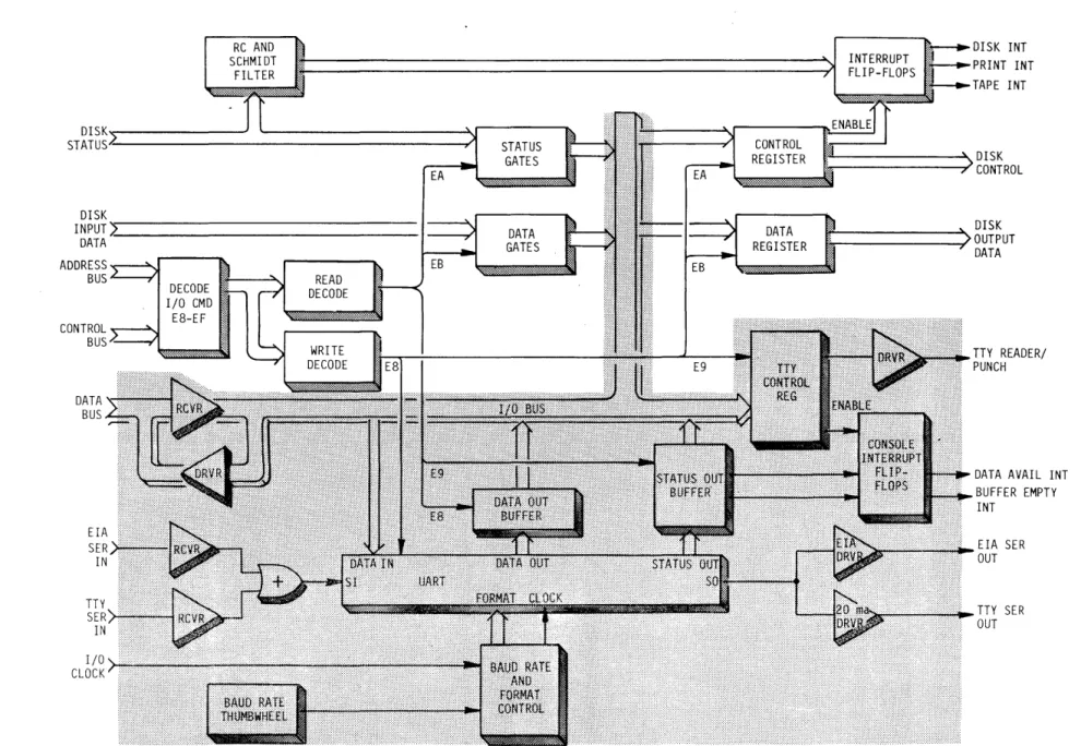
CONSOLE I/O This section, shown in Figure 3-5, provides both
a limited EIA RS-232 serial interface and a TTY current loop interface. However, only one terminal can be connected to the board at any time. A UART is the heart of the circuit, providing parallel to serial and serial to parallel conversion, status, and programmable control functions. The UART clock rate and number of stop bits are switch-selected.
Serial data input received from the EIA receiver or the current loop inter-face is fed to the UART. The UART shifts the serial data in and sets the data available (OA) status when a complete character has been received. If interrupts are enabled, this triggers the TTY IN interrupt (level 4). The parallel data is enabled out of the UART through tri-state buffers onto the internal data bus is by reading port E8. This also resets OA.
Serial data out is transmitted by performing a write to port E8. The parallel data is presented to the UART from the internal bus and strobed into the UART by applying a pulse to its OS input. This initiates the serial output stream to an open collector driver for the TTY current loop inter-face and to a bipolar driver for the EIA interinter-face. When the character
is transmitted, TBMT (transmit buffer empty) is set by the UART. If
in-terrupts are enabled this sets the TTY OUT interrupt (level 5).
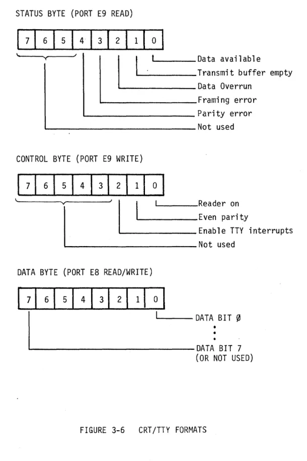
Status indications consisting of OA, TBMT, OR (overrun), FE (framing error) or PE (parity error) are available by reading port E9. Tri-state buffers
W
I
...
...
RC AND SCHMIDT
FIL TER
DIS ' C ' " ' - - - '
STAT U S ' - - - . , ... I
EA
DISK
INPUT ~ _ _ _ _ _ _ _ _ _ _ _ _ _ _ _ _ - - - - " 1
DATA ADDRESS - - c - - -...
BUS
CONTROL ~-... BUS'--oI"
~mmmS
FIGURE 3-5 MASTER CPU CONSOLE I/O
INTERRUPT FLIP-FLOPS
DISK INT PRINT INT TAPE INT
~ DISK
t : : r - - - T 7 CONTROL
~iimlEmmm;
DISK ~---~ OUTPUT
DATA
TTY READER/ PUNCH
DATA AVAIL INT BUFFER EMPTY INT
EIA SER OUT
STATUS BYTE (PORT E9 READ)
y
CONTROL BYTE (PORT E9 WRITE)
\71615141312\1101
\.. VI
L'
... _ _ _ _ _ Even parity _ R e a d e r onEnable TTY interrupts
~ ___________________ Not used
DATA BYTE (PORT E8 READ/WRITE)
1716\5141312\110\
I
'---
DATA. BIT 0.... - - - D A T A BIT 7
(OR NOT USED)
data and control ports are shown in Figure 3-6.
A TTY-related function is control of the TTY paper tape reader. A separate reader-on flip-flop and open collector driver provide the interface for
this function. The flip-flop is turned on ~nder program control and is
reset upon receipt of the start bit, thus reading a character at a time.
The status byte which controls the TTY paper tape reader, the UART parity circuits, and enables the TTY interrupts is output by a write to port E9.
The CONSOLE connector is a 25 pin connector conforming to ErA RS-232-C standards which is mounted on the development computer rear panel. This connector is connected to connector P2 on the top edge of the Master CPU board by a ribbon cable.
To interface to the CRT or other ErA peripherals, certain signals of the
RS-232-C interface are pulled up permanently to a logic 1. These signals
are clear to send, data set ready, carrier detected, data terminal ready, and request .to send.
DISK I/O The disk I/O logic, shown in Figure 3-7, consists
of a data I/O port, a control I/O port, and interrupt flip-flops. The byte
formats are shown in Figure 3~8. The eight disk input data bits (01 00-7)
are terminated with a pull up-pull down network and received with tri-state
buffers. The ~uffers are gated onto the internal bus by reading port EB.
Output data is stored in an eight-bit register by writing to port EB. The
outputs are driven with tri-state buffers. Disk status input is enabled
to the data bus with tri-state drivers by reading port EA. Disk controller
signals PBZY and FLG are filtered with an RC network and shaped by a Schmitt trigger, then fed to interrupt flip-flops. A paper tape signal is provided for replacement of the disk drives by a high speed paper tape reader. Disk
control is performed by a write to port EA. This outputs a control byte
which consists of the three disk control bits, a spare output bit and
terrupt enables for the disk and printer. The three output disk control
.
bits are buffered with tri-state drivers.For a detailed description of the floppy disk command formats and timing refer to Appendix A.
I/O DECODING The I/O decoding logic, shown in the shaded por-tion of figure 3-9, recognizes extended I/O commands to addresses E8-EF. The logic provides enable lines for the tristate input gates and clocks for the output registers. The logic also provides strobes for the bank switch and timer interrupt control discussed in other sections.
3.2.3 Interrupt Logic The interrupt 1 ogi c, shown in Fi gure 3-10,
resolves priority and generates the interrupt routine address vector for
16 system interrupts. It also handles the interaction of the 16 level
Debug interrupt vector generator.
Interrupts are levels created by a dedicated interrupt flip-flop. The 16
interrupt lines are continuously sampled at a 10 MHz rate. If one or more interrupts are present, the CPU interrupt line is activated. When the CPU responds with INTACK, sampling is stopped and the interrupt address for the highest priority line present is encoded. The vector is placed on the data bus during INTACK for input to the CPU. I/O circuits can also recognize their vector on the data bus during INTACK to determine when their inter-rupt request has been acknowledged. On~board interrupts are reset with a vector decoder which is enabled during INTACK. The Debug module interrupts have lower priority and are given an enable line (DBG V~N) only if no system I/O interrupts are pending. Figure 3-11 lists priorities and vector ad-dresses for the interrupts.
3.2.4 DMA Logic DMA operati ons requi re that the CPU be paused, and
W
I
~
U1
E9
E8
DATA IN UART TTY
SE R >---1 IN
I/O
CLOCK ) - - - 1 - . . 1 BAUD RATE AND BAUD RATE
THUMBWHEEL
FORMAT CONTROL
E9 TTY
CONTROL REG
INT
INT
:JIr--... TTY READER/
PUNCH
ENABr-:-LE=-_ _
CONSOLE
iNTERRU D---II.DATA AVAIL
ITg---l~. FLIP- INT
FLOPS BUFFER EMPTY
INT
~ _ _ _ ~_EIA SER OUT
L..---I''-v ""'~ _ _ _ --II_ TTY SE R
OUT
DATA BYTE (READ/WRITE PORT EB)
17
1
6 51
41
31
21
11.
01
\. )
'-"
I
" ' " ' - - - Binary Data STATUS-BYTE (READ PORT EA)
17
I
61
51
41
31
21
11
0I
\.. ... )
I
I
""""'-_ _ _ P ri nt e r
'---_ _ _ _ Printer Fault = 0
a..-_ _ _ _ _ _ _ _ _ Not Used = Always 1
"'"'--_ _ _ _ _ _ _ _ _ _ _ _ _ Fl ag
=
1CONTROL BYTE (WRITE PORT EA)
17161514131211101
~
I
I
_______
~RB
_ _ _ _ _ _ _ _ CTRL (not used)
____________ Enable disk interrupt _ _ _ _ _ _ _ _ _ _ _ Enable printer interrupt _ _ _ _ _ _ _ _ _ _ _ _ _ Not used
W I ... ... DISK STATUS EIA SER)>----I IN
RC AND SCHMIDT
FIL TER
EA
EB
E8
DATA IN
SI UART
1/0
CLOCK~---~~
BAUD RATE THUMBWHEEL
STATUS GATES
DATA GATES
BAUD RATE AND FORMAT CONTROL EB E9 CONTROL REGISTER DATA REGISTER TTY CONTROL REG
DISK INT
INTERRUPT PRINT INT
FLI P-FLOPS
TAPE INT
ENABL DISK CONTROL DISK OUTPUT DATA
.k--~ TTY READER/ PUNCH
ENABr.;.L E::.-_ _
CONSOLE INTERRU
FLIP-FLOPS
_---1~DATA AVAIL INT
_--I~ BUFFER EMPTY INT
, , - - - 1 __ .. _ ~~ _ _ _ ... EIA SER OUT
L---I''-v '"' ... k---I~ TTY SE R
OUT
MSTR PAUSE and drives the PAUSE input of the 2650. After completion of the current instruction, the 2650 RUN output will go high. This is used to disable the address and data bus drivers, which float the buses.
3.2.5 Baud Rate and Timer Logic The block diagram of this section
is shown in Figure 3-12.
A crystal-controlled oscillator, identical (except for frequency) to that used in the CPU clock logic, is used for the baud rate and interval timer generators. The 9.984 MHz output of the oscillator is directed through a driver to the rest of the system through the system bus. The 38.4 KHz system I/O clock is provided by a divide by 260 circuit off the 9.984 MHz crystal. This is further divided by two and splits into three paths. One chain of dividers provides the 150-2400 (x16) baud rate clocks. The second path is a divide by eleven providing the I/O baud TTY rate. The third chain is a divide by 24 or 240 providing 10 or 100 ms interval timer clock.
3.3 UTI LIZATION
3.3.1 Installation The module is designed to be plugged into the
card file of the development computer, but may be used in other applica-tions. Jumper and switch options are discussed in section 3.3.2. All inter-face connections and connector pinouts are detailed in section 3.3.3.
COMPUTER INSTALLATION The Master CPU module plugs into any
Master section slot of the motherboard (J3-J8). For cabling convenience, it is normally plugged into J8. The car