degree of
Doctor of Philosophy
CALIFORNIA INSTITUTE OF TECHNOLOGY
Pasadena, California
2017
ii
© 2017
Amirreza Safaripour ORCID: 0000-0001-9758-6156
iv
ACKNOWLEDGEMENTS
Pursuing a doctoral degree is an extremely long yet rewarding journey and if it was
not for the help and support of numerous individuals, I would have not been able to
get to this point. During this journey, I truly learned how profoundly the interactions
with people we come across with in life can shape our mind, and lead to significant
changes in our future opportunities.
Mr. Farhad Saber and Mr. Ali Roshan, who taught me several courses in
mathe-matics during high school, were two of such people in my life. With their incredible
teaching methods, they taught me how to approach math problems correctly, enjoy
solving them, and always look for more problems to solve. They guided me to
develop an engineering mindset for which I am always thankful to them.
After I was admitted to Sharif University of Technology for my undergraduate
studies, it was the one and only Prof. Sharifbakhtiar’s electronics classes that left
no doubt for me that THIS was what I wanted to do for my entire life. I truly fell
in love with electronics through his lectures. In his classes, not only did we explore
the astonishing world of electronics, but also I learned engineering discipline and
professional commitment, which has stuck with me ever since and I am always
grateful for it. Also, I was fortunate enough to work with Prof. Fotowat as his
teaching assistant for many of the classes he taught. I learned precious lessons in
science and life from him during the unforgettable meetings we had. The numerous
good memories and jokes from our discussions will stay with me forever. I would
like to thank him for all the academic and professional support he provided for me
during my studies at Sharif which were essential to navigate me to Caltech.
I am proud to have worked with Prof. Ali Hajimiri as my advisor at Caltech, who
has truly been a source of inspiration for me. He always encouraged me to explore
new ideas and challenges and taught me to think outside the box and to focus on
innovation and long-term impact. He always believed in me during the ups and
downs of my research, and through his encouragements he infused confidence in
me to push my own boundaries. Due to his unique way of managing the group, we
all count on him both as an advisor and as a friend. In addition to the invaluable
technical advice, Ali has provided me with a great deal of support and guidance on
a personal level as well, and during the difficult times he was like an elder brother
I would like to specifically thank my former labmates Steve and Kaushik (K2) for
their true friendship and great help, as well as the invaluable lessons I learned from
them through countless technical discussions we had. The unforgettable memories
from all the fun activities as well as the sleepless nights during the several tapeouts
will always remain with me. I would also like to thank all current and former
members of CHIC lab whom I had the pleasure of working with, including Behrooz,
Florian, Costis, Kaushik (K1), Firooz, Alex, Matan, Aroutin, Brian, Reza, Parham,
Elliott, Austin, Chris, and M. Reza, as well as the current and former members
of MICS lab who helped me a great deal over these past years, including Manuel,
Meisam, Saman, Juhwan, Mayank, Matt, Krishna, Abhinav, Milad, and Aryan. I
would like to extend my gratitude to our group administrator, Michelle, for her
continued support, and our department administrators, Tanya and Carol, who have
always been kind and helpful. I would also like to especially thank Laura and Daniel
for making Caltech a welcoming place for me as an international student.
I did not have the chance to visit home during my studies at Caltech, and
unfortu-nately my family could not come here for visit either. In this situation, looking back
at all the ups and downs over these past years, there is no doubt that it would not
have been possible to survive the graduate life if it was not for my beloved friends
here in Southern California. I have had the fortune of knowing Paniz, Mohammad,
Tina, Ashkan, Maani, Hannaneh, Nariman, Hessam, and Mahsa, who have always
been there for me with genuine love and continuous support whenever I needed
them. They are indeed more than just my friends. To me, they are family and I will
always be thankful to them for all the help, love, and good memories. Also, a tip
of hat to all my good friends across the globe, particularly Negar, Alborz, Rozhin,
Bahram, Mahdi, Niloufar, Azadeh, Hamidreza, Parinaz, Javad, Gilda, Diana, Amer,
Babak, Yasamin, Jamshid, Hengameh, Ardalan, Behnaz, Hassan, and Paniz, who
vi
Finally and most importantly, I would like to thank my parents for their endless love
and unconditional support in every single step I took in my entire life, and for the
opportunities they provided for me to pursue my dreams. None of this would have
been possible if it was not for them. I cannot thank them enough for their patience
and encouragements throughout these years. I’m also thankful to my brother, Ali,
for always paving the path for me so that I can easily follow his lead, and to my little
sister, Samira, whose love and energy have always been the strongest driving force
excited substrate modes in the dielectric substrate of an integrated antenna
con-tain valuable information regarding its far-field radiation properties. We introduce
Proximal-Field Radiation Sensors (PFRS) as a number of small sensing antennas
that are placed strategically on the same substrate as the integrated antenna and
measure electromagnetic waves in its immediate proximity. These sensors extract
the existing information in the substrate modes and use it to predict the far-field
radiation properties of the integrated antenna in real-time based on in-situ
measure-ments in the close proximity of the antennas, without any need to use additional
test equipment and without removing the antenna from its operating environment
or interfering with its operation in a wireless system. In other words, PFRS enables
self-calibration, self-correction, and self-monitoring of the performance of the
inte-grated antennas. Design intuition and a variety of data processing schemes for these
sensors are discussed. Two proof-of-concept prototypes are fabricated on printed
circuit board (PCB) and integrated circuit (IC) and both verify PFRS capabilities in
prediction of radiation properties solely based on in-situ measurements.
Dynamically controllable integrated radiators would significantly benefit from PFRS.
These radiators are capable of controlling their radiation parameters such as
polar-ization and beam steering angle through their actuators and control units. In these
cases, PFRS serves as a tool for real-time monitoring of their radiation parameters, so
that without direct measurement of the far-field properties through bulky equipment
the required information for the control units and the actuators are provided.
Dynamically controllable integrated radiators can be designed using the additional
design space provided by Multi-Port Driven (MPD) radiator methodology. After
a review of advantages of MPD design over the traditional single-port design, we
show that a slot-based MPD radiator would have the additional advantage of reduced
viii
demonstration of a 134.5-GHz integrated slot-based MPD radiator with a measured
single-element EIRP of+6.0 dBm and a total radiated power of−1.3 dBm.
We discuss how MPD methodology enables the new concept of Dynamic
Polar-ization Control, as a method to ensure polarPolar-ization matching of the transmitter
antenna to the receiver antenna, regardless of the polarization and orientation of the
receiver antenna in space. A DPC antenna design using the MPD methodology is
described and a 105.5-GHz 2×1 integrated DPC radiator array with a maximum
EIRP of +7.8 dBm and a total radiated power of 0.9 mW is presented as the first demonstration of an integrated radiator with DPC capability. This prototype can
control the polarization angle across the entire tuning range of 0◦ to 180◦ while
maintaining axial ratios above 10 dB, and control the axial ratio from 2.4 dB (near
circular) to 14 dB (linear). We also demonstrate how simultaneous two-dimensional
beam steering and DPC capabilities can even match the polarization to a mobile
receiver antenna through a prototype 123-GHz 2×2 integrated DPC radiator array
with a maximum EIRP of +12.3 dBm, polarization angle control across the full range of 0◦to 180◦as well as tunable axial ratio down to 1.2 dB and beam steering
of up to 15◦in both dimensions. We also use slot-based DPC antennas to fabricate
a 120-GHz integrated slot-based DPC radiator array, expected to have a maximum
EIRP of+15.5 dBm.
We also introduce a new modulation scheme called Polarization Modulation (Pol-M)
as a result of DPC capability, where the polarization itself is used for encoding the
data. Pol-M is a spatial modulation method and is orthogonal to the existing phase
and amplitude modulation schemes. Thus, it could be added on top of those schemes
to enable creation of 4-D data constellations, or it can be used as the only basis for
modulation to increase the stream security by misleading the undesired receivers.
We discuss how DPC antenna enables Pol-M and also present PCB prototypes for
polarization control of two-dimensional integrated phased arrays”, IEEE Transactions on Microwave Theory and Techniques, vol. 64, no. 4, pp. 1066– 1077, Apr. 2016. doi:10.1109/TMTT.2016.2530704,
A. Safaripour authored the manuscript, performed the system measurements, and was responsible for the electromagnetic design of the antennas, passives, and matching networks, as well as the entire integrated circuitry other than the distribution network and the digital to analog converters, which were designed by S. M. Bowers and K. Dasgupta, respectively.
[3] ——, “A 2×2 dynamic polarization-controlling integrated phased array”, in IEEE Radio Frequency Integrated Circuits Symposium (RFIC), May 2015, pp. 219–222. doi:10.1109/RFIC.2015.7337744,
A. Safaripour authored the manuscript, performed the system measurements, and was responsible for the electromagnetic design of the antennas, passives, and matching networks, as well as the entire integrated circuitry other than the distribution network and the digital to analog converters, which were designed by S. M. Bowers and K. Dasgupta, respectively.
[4] S. M. Bowers, A. Safaripour, and A. Hajimiri, “Dynamic polarization con-trol”, IEEE Journal of Solid-State Circuits, vol. 50, no. 5, pp. 1224–1236, May 2015. doi:10.1109/JSSC.2015.2403313,
A. Safaripour designed the entire drive and control circuitry including the oscillators, amplifiers, phase rotators, locking network, as well as electro-magnetic structures such as inductors and matching networks, and partici-pated in the writing of the manuscript, while S. M. Bowers was responsible for the electromagnetic design of the array, performance analysis, system measurements, and preparing the manuscript.
[5] ——, “An integrated slot-ring traveling-wave radiator”,IEEE Transactions on Microwave Theory and Techniques, vol. 63, no. 4, pp. 1154–1162, Apr. 2015. doi:10.1109/TMTT.2015.2405921,
x
manuscript while S. M. Bowers was in charge of the antenna design, system measurements, and preparing the manuscript.
[6] ——, “Dynamic polarization control of integrated radiators”, inIEEE Radio Frequency Integrated Circuits Symposium (RFIC), Jun. 2014, pp. 291–294. doi:10.1109/RFIC.2014.6851723,
A. Safaripour designed the entire drive and control circuitry including the os-cillators, amplifiers, phase rotators, locking network, as well as electromag-netic structures such as inductors and matching networks, and participated in the writing of the manuscript, while S. M. Bowers was responsible for the electromagnetic design of the array, system measurements, and preparing the manuscript.
[7] ——, “An integrated traveling-wave slot radiator”, in IEEE Radio Fre-quency Integrated Circuits Symposium (RFIC), Jun. 2014, pp. 369–372. doi:10.1109/RFIC.2014.6851744,
A. Safaripour was responsible for the entire integrated circuit design includ-ing the oscillator and amplifiers, as well as the electromagnetic design of the passives and matching networks, and participated in the writing of the manuscript while S. M. Bowers was in charge of the antenna design, system measurements, and preparing the manuscript.
[8] S. Bowers, K. Dasgupta, A. Safaipour, and A. Hajimiri,Dynamic polariza-tion modulapolariza-tion and control, US Patent 9,485,076, Nov. 2016,
A. Safaripour participated in the conception of the idea, the design of proof-of-concept architectures, and the writing of the manuscript.
[9] S. Bowers, A. Safaripour, and A. Hajimiri,Sensing radiation metrics through mode-pickup sensors, US Patent App. 13/766,667, Mar. 2014,
A. Safaripour participated in the conception of the idea, designed proof-of-concept architectures, developed the data analysis methods, and participated in the writing of the manuscript.
[10] M. Varonen, A. Safaripour, D. Parveg, P. Kangaslahti, T. Gaier, and A. Hajimiri, “200-GHz CMOS amplifier with 9-dB noise figure for atmospheric remote sensing”,Electronics Letters, vol. 52, no. 5, pp. 369–371, Mar. 2016. doi:10.1049/el.2015.3337,
A. Safaripour was responsible for designing the device layout methodology for optimal high-frequency performance.
xii
CONTENTS
Acknowledgements . . . iv
Abstract . . . vii
Published Content and Contributions . . . ix
Contents . . . xii
List of Figures . . . xiv
List of Tables . . . xxviii
Chapter I: Introduction . . . 1
1.1 Contributions . . . 2
1.2 Organization . . . 3
Chapter II: Integrated Antennas: Motivations and Challenges . . . 5
2.1 Integrated Antennas for Wireless Systems . . . 5
2.2 Surface Waves in Integrated Antennas Substrate . . . 8
2.3 Effects of Process and Environmental Variations . . . 11
2.4 Indirect Measurement of Far-Field Radiation Properties . . . 13
Chapter III: Proximal-Field Radiation Sensors . . . 18
3.1 Introduction . . . 18
3.2 Integrated Antennas on Dielectric Substrates . . . 19
3.3 Proximal-Field Sensing . . . 22
3.4 PFRS Data Capture Fundamentals . . . 29
3.5 PFRS Data Processing . . . 42
3.5.1 Symmetry-based Methods . . . 43
3.5.2 Statistical Methods . . . 54
3.5.3 Simulation-based Methods . . . 58
3.6 PFRS Implementation on a PCB prototype . . . 64
3.6.1 Prototype Design . . . 65
3.6.2 Data Interpretation . . . 65
3.6.3 Measurements . . . 69
3.7 PFRS Implementation on an IC prototype . . . 72
3.7.1 System Architecture . . . 73
3.7.2 Radiator Design . . . 75
3.7.3 PFRS Design . . . 79
3.7.4 Measurements . . . 81
3.8 Conclusions . . . 84
Chapter IV: Multi-Port Driven Antennas . . . 87
4.1 Introduction . . . 87
4.2 Multi-Port vs. Single-Port Antennas . . . 88
4.2.1 Limitations of Single-Port Antennas . . . 89
4.2.2 Advantages of Multi-Port Antennas . . . 90
5.3.3 A 2×1 Integrated DPC Radiator Array . . . 124
5.3.4 A 2×2 Integrated DPC Radiator Array . . . 141
5.3.5 A 2×2 Integrated Slot-Based DPC Radiator Array . . . 163
5.4 Polarization Modulation . . . 165
5.4.1 Prototype: Transmitter and Receiver Architectures for Pol-M 170 5.4.2 Pol-M with the 2×2 Integrated DPC Radiator Array . . . 175
5.5 Conclusions . . . 175
Chapter VI: Conclusions . . . 177
xiv
LIST OF FIGURES
Number Page
2.1 Operation principle of Distributed Active Radiator (DAR) [5]. . . 6
2.2 Block diagram of the Multi-Port Driven (MPD) antenna [6]. . . 6
2.3 Die photo of the (a) transmitter chip and (b) receiver chip for a
coherent imaging system [8]. . . 7
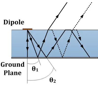
2.4 Transmitting antenna on a dielectric substrate showing the rays trapped
as surface waves with the critical angleθC =30◦appropriate for fused quartz (r =4) [23]. . . 8 2.5 Normalized power versus substrate thickness for (a) dipole on quartz
substrate, (b) dipole on silicon or GaAs substrate, (c) slot on quartz
substrate, and (d) slot on silicon or GaAs substrate [22]. . . 9
2.6 Operation of a silicon lens to minimize substrate modes and to radiate
the highest power down through the bottom of the substrate [12]. . . . 10
2.7 3-D depiction of the use of a dielectric superstrate (quartz in this case)
to couple electromagnetic power up from the metal stack to antennas
printed on top of the superstrate [17]. . . 10
2.8 Average number dopant atoms as a function of technology node [33]. 12
2.9 Line edge roughness shown in SEM images of an example process
[35]. . . 12
2.10 Threshold voltage variation over technology node [36]. . . 12
2.11 Exterior fields of radiating antenna [40]. . . 14
2.12 Specific expressions for scanning with ideal dipole on a plane,
cylin-der, and sphere [40]. . . 15
2.13 Magnetically coupled in-situ probes for patch antennas operating at
20 GHz [45]. . . 16
3.1 Generation of surface waves inside the direlectric substrate of an
integrated antenna. . . 19
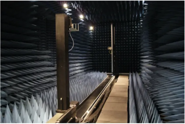
3.2 Compelexity of an exemplary far-field measurement setup for a
mm-wave integrated radiator operating at 120 GHz. . . 20
3.3 A simplified diagram for a far-field measurement range with AUT
used as the receiver antenna and a known antenna used as the
multi-port PFRS antennas. . . 25
3.10 Possible undesired mechanisms that could affect PFRS performance:
(a) coupling tp strongly driven points by the drive circuitry and (b)
incident electromagnetic on the system from external sources. . . 26
3.11 Amplitude read-outs of the PFRS antenna located at the center versus
the relative phase difference between the two radiating antennas. . . . 27
3.12 Arrange of metallic contacts in the simulation setup to evaluate
cou-pling of PFRS to strongly driven points on the chip. . . 27
3.13 Coupling strength of all PFRS antennas to the driving signal
ampli-tude at the strongly driven points through substrate. . . 28
3.14 Simulation setup for evaluation of PFRS sensitivity to
electromag-netic waves incident on the chip from a half-wavelength dipole
an-tenna placed at 2λdistance above the chip. . . 28 3.15 Signals picked up by PFRS antennas for 0 dBm input power to the
dipole antenna. . . 29
3.16 Rectangular waveguide configuration to evaluate various types of
PFRS antennas when three PFRS units are located at points L, C,
and R. . . 30
3.17 Field components of the first ten propagating waveguide modes across
the dashed line on top surface. . . 31
3.18 Y-oriented linear-slot antenna used as PFRS. . . 32
3.19 Outputs of the Y-oriented slots versus frequency for each excited mode. 33
3.20 X-oriented linear-slot antenna used as PFRS. . . 34
3.21 Outputs of the X-oriented slots versus frequency for each excited mode. 35
3.22 Field components of the first ten propagating waveguide modes across
xvi
3.24 Outputs of the Y-oriented dipoles versus frequency for each excited
mode. . . 38
3.25 Combined TE/TM sensor for the waveguide. . . 39
3.26 Outputs of the TE/TM sensors versus frequency for each excited mode. 40
3.27 Hertzian dipole excitation on a chip with (a) TE sensors and (b) TM
sensors. . . 41
3.28 (a) Outputs of the TE sensors and (b) outputs of the TM sensors for
Hertzian dipole excitation. . . 41
3.29 A 2×1 multi-port driven radiator array with 13 slot-ring PFRS antennas. 43
3.30 In-phase drive of the transmitting antennas for optimum broadside
radiation. . . 44
3.31 Simulated paterns of (a) gain and (b) directivity for optimum
broad-side radiation. . . 44
3.32 Simulated gain of the 2×1 array with relative phase error of (a) θ = +40◦and (b)θ = +40◦whileΦQ A=ΦQ A =0◦. . . 45
3.33 Outputs of the PFRS antennas vurses the relative phase error,θ, and the color codes for the outputs of each PFRS. . . 46
3.34 Difference between the signals at the left and right ports of the central
PFRS antenna. . . 47
3.35 Circular symmetry of the electromagnetic structure. . . 47
3.36 Outputs of the PFRS antennas versus quadrature phase errorΦQ Ain
Radiator Aand the color codes for the outputs of each PFRS. . . 48
3.37 A 2×2 multi-port driven integrated radiator array with nine slot-ring
multi-port PFRS antennas. Due to circular symmetry, the total 36
PFRS outputs can be divided into nine sets where all four output ports
in each set are expected to have the exact same signal. . . 49
3.38 Sensitivity of the standard deviations of all nine sets to the relative
phase errorθD. . . 50 3.39 Sum of the standard deviations for all nine sets as well as the relative
strength of the radiated signal asθD varies. . . 51 3.40 A 2×2 multi-port driven integrated radiator array with 13 PFRS
antennas. . . 51
3.41 Switching between horizontal and vertical polarization of the radiated
3.45 Example of Principal Component Analysis (PCA) ona 2-D data set. . 55
3.46 Magnitude of the principal components associated withθDcalculated using (a) both phases and amplitudes and (b) only amplitudes of the
PFRS read-outs. . . 57
3.47 Application of an exemplary phase error correction algorithm to a
random combination of relative phase errors θA, θB, θC, and θD, using the first principal component for each parameter. . . 57
3.48 Sniff antenna. . . 59
3.49 Example of an electromagnetic simulation setup using orthogonal
dipole sniff antennas with the integrated radiator chip to extract
math-ematical relationships required for pattern prediction. . . 60
3.50 Comparison between the normalized predicted pattern using
simu-lated PFRS read-outs and normalized simusimu-lated pattern by HFSS in
(a)φ= 0◦and (b) φ=90◦planes for broadside radiation. . . 62 3.51 Comparison between the normalized predicted pattern using
simu-lated PFRS read-outs and normalized simusimu-lated pattern by HFSS in
(a)φ= 0◦and (b) φ=90◦planes for off-axis radiation. . . 62 3.52 Arrangement of sniff antennas on a planar surface on top of the
integrated radiator chip in simulation to be used for plane-wave
de-composition. . . 64
3.53 (a) Heat map for the relative magnitude of the reconstructed electric
field on the planar surface using sniffers’ voltages and (b)
decompo-sition of the field into plane waves propagating at different angles,
showing a maximum at fx = fy =0, i.e. broadside radiation. . . 64 3.54 The prototype PCB antenna array with two transmitting patch
xviii
3.55 Symmetrically-placed sensors to detect the phase difference between
the driving signals of the two patch antennas. . . 66
3.56 Simulation setups to relate PFRS read-outs to the polarization of
radiated field (a) in an arbitrary direction, and (b) across an entire plane. 67
3.57 Simulation setup to investigate the impact of a disturbing metallic
reflector on the performance of PFRS: (a) 3-D view and (b) top view. 68
3.58 Comparison of the reflector impact on the normalized gain patterns
for φ = 90◦ plane based on (a) HFSS simulation and (b) prediction by simulated PFRS read-outs. . . 68
3.59 Measured and simulated input reflection coefficients of (a) the patch
and (b) PFRS antennas. . . 69
3.60 PFRS performance is evaluated through comparison between (a)
sim-ulation of radiation pattern through HFSS, (b) direct measurement of
radiation pattern in a far-field measurement setup, and (c) prediction
of radiation pattern through measured PFRS read-outs. . . 70
3.61 Normalized simulated, measured, and predicted gain patterns based
on PFRS read-outs in (a) φ=0◦and (b)φ= 90◦planes for in-phase drive. . . 71
3.62 Normalized simulated, measured, and predicted gain patterns based
on PFRS read-outs in φ = 90◦ plane for (a) 90◦, (b) −90◦ and (c) 180◦of phase difference between the patch antennas. . . 71
3.63 Normalized simulated, measured, and predicted (a) co-polarization
and (b) cross-polarization gain patterns inφ= 90◦plane for in-phase drive. . . 72
3.64 Measured and simulated amplitude response ofS1andS2. . . 72
3.65 Simplified block diagram of the 2×1 integrated linear-slot radiator
with four PFRS antennas. . . 73
3.66 Detailed block diagram of the 2×1 integrated linear-slot radiator with
four PFRS antennas. . . 74
3.67 (a) Electromagnetic structure of the 2×1 integrated linear-slot radiator
and (b) simulated gain pattern. . . 75
3.68 (a) Electromagnetic structure of the integrated radiator’s packaging
and (b) simulated gain pattern. . . 76
3.69 (a) Schematic of the quadrature oscillators and (b) the simulated
3.74 Simulated magnitude of the signals picked up by PFRS antennas
when the phase difference between the two antennas is swept from
0◦(setting index = 0) to 360◦. (setting index = 16) . . . 80
3.75 Downconversion scheme for coherent detection of PFRS signals. . . . 80
3.76 (a) LO distribution network to PFRS locations for downconversion
and (b) detection circuitry located next to PFRS antenna. . . 81
3.77 Circuit schematics for (a) mixerM1, (b) mixerM2, (c) amplifier at f0,
(d) mixerM3, and (e) buffer for distribution of off-chip low-frequency
reference at f0. . . 82
3.78 Measurement of the radiation frequency of the 2×1 integrated
linear-slot radiator array versus the tuning voltage of the quadrature oscilaltors. 83
3.79 Comparison between calibrated measured read-outs of PFRS for both
I and Q channels of each sensor and simulated downconverted signals
versus the phase difference between the two radiating antennas. The
difference between two consequent phase rotator settings is roughly
equal to 22.5◦. . . 83 3.80 Electromagnetic simulation setup to extract relationship between
PFRS antennas and far-field radiation pattern ofEθ inφ=0◦plane. . 84 3.81 Normalized simulated gain pattern from HFSS and predicted gain
pattern based on measured PFRS read-outs in (a) φ = 0◦ and (b) φ = 90◦ planes for 0◦ phase difference between the two linear-slot
antennas. . . 85
3.82 Normalized simulated gain pattern from HFSS and predicted gain
pattern based on measured PFRS read-outs in (a) φ = 0◦ and (b) φ=90◦planes for+90◦phase difference between the two linear-slot
xx
3.83 Normalized simulated gain pattern from HFSS and predicted gain
pattern based on measured PFRS read-outs in (a) φ = 0◦ and (b) φ=90◦planes for−90◦phase difference between the two linear-slot antennas. . . 85
4.1 Example of traditional single-port radiator with lossy matching
net-works and independent design of individual blocks [6]. . . 88
4.2 Multi-port driven radiator design methodology for integrated
radia-tion where drivers directly feed multiple ports of the antenna [6] . . . 89
4.3 Example of EM duality for a dipole antenna, with the cross-section
of the beam, and E and H fields shown. The dual complement of this is the slot dipole, where the series source of the dipole has been
replaced with an orthogonal source across the slot, and theEandH fields have been normalized and swapped. . . 92
4.4 Electromagnetic Duality for the MPD slot ring antenna converts a
four-series port wire ring antenna into a four-port slot ring driven in
quadrature, producing a traveling wave around the ring and circular
polarization in the far field. . . 93
4.5 Current distribution on the four-series port ring antenna when two of
the ports are at their maximum amplitude, while the other two have
zero amplitude. This current distribution then rotates around the ring
in a traveling-wave fashion over one oscillation period. . . 94
4.6 3-D depiction of the traveling-wave slot radiator, with quadrature
driver circuitry at the center of the chip that drives across the metal
slot at four ports. The inner ground plane extends orthogonally across
the slot out to the edge of the chip to provide a bond pad to sink the
dc current, and the outer ac ground plane is biased at VDD to provide
dc power to the driver circuitry through the antenna feeds. . . 95
4.7 Block diagram showing the driver circuitry and the slot ring antenna.
A quadrature oscillator sits at the center of the chip and is amplified
through three buffer amplifier stages before being routed out to the
antenna ports across the slot. . . 97
4.8 Schematic of the quadrature voltage-controlled oscillator (VCO),
which generates the four required phases by coupling two
cross-coupled VCOs through two coupling mechanisms. (a) Resistive
net-work at the tails (RC = RT = 10Ω). (b) Weak quadrature coupling
nature of the coupling between different segments of the inductor.
Component values are optimized by Agilent ADS to minimize
mod-eling error. . . 101
4.12 Comparison between S-parameters of the EM simulation of the
in-ductor and S-parameters of the optimized equivalent-circuit model
of the inductor. The circuit model is well matched to EM simulation
over a wide frequency range. . . 102
4.13 Equivalent-circuit model is used with extracted layout of quadrature
oscillator’s transistors and resistors to simulate oscillation frequency. 102
4.14 Simulated output waveforms of the quadrature oscillator. Quadrature
waveforms verify correct operation of the two coupling mechanisms. 103
4.15 Schematic of the amplifier chain consisting of three cascode stages
with 20-, 40-, and 60-µm widths,respectively. . . 104 4.16 Die photograph of the traveling-wave slot ring radiator with a
break-out view of the antenna, driver circuitry, and areas of fill exclude. . . 105
4.17 Device packaging to enable wire-bond connection of dc supply while
radiating out from the backside of the chip. . . 105
4.18 Measurement setup for the traveling-wave slot radiator for: (a)
abso-lute power calibration and (b) spectral measurement. . . 106
4.19 Measured calibrated spectrum of the received signal shows−25.1-dBm captured power, which corresponds to an EIRP of 6.0 dBm at 134.5 GHz
when considering the distance and gain of the receive antenna. . . 107
4.20 Orthogonal elevation planes of the simulated and measured radiation
xxii
5.1 Effects of polarization mismatch on coupling transmit/receive
an-tenna pairs. Maximum coupling occurs for polarization matched
antenna pairs (top), no coupling for completely mismatched pairs
(middle) and partial coupling for partially mismatched pairs (bottom). 112
5.2 Definitions of the polarization parameters for the general elliptical
polarization. . . 114
5.3 Examples of polarization mismatch in wireless communication links:
(a) due to antenna mismatch, (b) due to orientation change between
the transmitter and receiver in mobile systems. . . 115
5.4 A radiator with Dynamic Polarization Control (DPC) can transmit any
polarization angle and polarization axial ratio in order to maintain
polarization matching with a receive antenna of any polarization or
orientation in space. . . 116
5.5 (a) DPC antenna ensures polarization matching between the
trans-mitter and receiver regardless of receiver antenna type and (b) solves
polarization mismatch in mobile systems when used in 2-D phased
arrays. . . 117
5.6 Four-spoke Multi-Port Driven (MPD) antenna for dynamic
polariza-tion control. . . 118
5.7 Operation principle of the original DPC antenna based on
superpo-sition of two orthogonal linear polarizations. . . 119
5.8 Realization of any arbitrary elliptical polarization with two
orthogo-nal linear polarizations, as well as (b) graphical representation of the
extreme cases of linear and (c) circular polarizations. . . 120
5.9 Modified MPD antenna of circumference gλ used for polarization control. The phases and amplitudes of the drives of spokes A and B
are controlled independently from each other, while ports on opposite
ends of each spoke are driven differentially with the same amplitude. 121
5.10 Analysis setup for superposition subpart A when broken up to
con-sider just (a) the signal ring or (b) just the spokes. The port impedances
from subpart B are in parallel to the virtual shorts and thus do not
affect the current distribution due to subpart A. . . 122
the antennas. . . 126
5.14 Schematic of the central QVCO with two coupling mechanisms:
Re-sistive network at the tail (Rc = Rt = 15Ω) and quadrature coupling
through transistors (WMq =0.5µm,WMc = 20µm). The “Y” resistive network can be simplified through its “∆” equivalent for analysis. . . 128
5.15 Simulated phase noise at 1 MHz offset and the ratio of second
har-monic to fundamental of the QVCO vs. coupling resistance (Rc0) for
three different widths (0.5µm, 1µm, 1.5 µm) of coupling transistors along with the time-domain waveforms for R0c =0ΩandR
0
c =40Ω
whenWMq = 0.5µm. . . 129 5.16 Schematic of Gilbert cell based phased rotator. In-phase and
quadra-ture signals from the locking network are weighted arbitrarily and
added in current domain to generate the desired output phase to lock
cores’ oscillator (W = 2 µm for tail transistors,W =1 µm for upper transistors). . . 131
5.17 Simulated output current of phase rotator for eight different settings.
Control voltages are set to generate 45◦separated phases while
keep-ing the amplitudes constant. . . 131
5.18 Schematic of the amplifier chain consisting of a differential
common-source stage (W = 5 µm) and two differential cascode stages (W = 15 µm andW =30 µm). Gain of the chain is controlled through the biasing circuit. . . 132
5.19 Additional non-idealities including the effects of extending the spokes
xxiv
5.20 Simulated radiation gain pattern of the 2×1 array in circularly
po-larized mode and linearly popo-larized mode for planes φ = 0◦(a) and φ=90◦(b) show similar patterns and maximum gains within 0.3 dBi of each other. . . 135
5.21 Measurement setup for the 2×1 radiator with DPC. . . 136
5.22 Calibrated measured spectrum of the DPC radiator array in linearly
polarized mode has a maximum EIRP of+7.8 dBm at 105.5 GHz. . . 137 5.23 Measured radiation pattern for two elevation planes whenφ= 0◦(a)
and φ = 90◦ (b) for broadside radiation as well as beam steering in both directions in theφ= 0◦dimension. . . 137 5.24 Orientation of coordinate system (a) as well as three directions used
in demonstration of DPC: θ = 0◦ (b), θ = 20◦, φ = 0◦ (c), and θ =30◦, φ=90◦(d). . . 138 5.25 Two demonstrations of DPC: tuning of the polarization angle while
maintaining linear polarization (a), and tuning of the axial ratio while
maintaining constant polarization angle (b). . . 139
5.26 Measured tuning of polarization angle while maintaining linear
po-larization (axial ratios above 10 dB) show full tuning range from 0◦
to 180◦in three different directions. . . 139
5.27 Measured tuning of polarization axial ratio while maintain near
con-stant polarization angles in three directions show tuning range from
2.4 dB through 14 dB. . . 139
5.28 Die photo of 2×1 radiator array with DPC. . . 140
5.29 Block diagram of the 2×2 DPC integrated phased array. . . 141
5.30 Modifications of the DPC antenna by adding two additional ground
spokes to allow low-loss transmission lines for the locking signals
while maintaining the symmetry of the structure. . . 142
5.31 Effect of the 5th and 6th spokes on polarization angle tuning. (a)
Polarization angle is set by the drive settings and the (b) simulated
polarization angle, (c) axial ratio, and (d) antenna array gain show
more accuracy and symmetry for six-spoke DPC antennas. . . 144
5.32 Effect of the 5th and 6th spokes on axial ratio tuning. (a) Axial ratio
is set by the phase difference of the drive sets, and the (b) simulated
polarization angle, (c) axial ratio, and (d) antenna array gain show
with independent phase and gain control units for the two subparts,
as well as independent control for each antenna with respect to the
other antennas in the array. . . 147
5.36 Detailed block diagram of the drive circuitry for each DPC antenna
with independent phase and gain control units for the two subparts,
as well as independent control for each antenna with respect to the
other antennas in the array. . . 148
5.37 Schematic of the buffer chain that controls the gain of each subpart in
the antenna drive circuitry with a maximum simulated gain of 10.2 dB.149
5.38 Variations of the single-ended input impedances of the DPC antenna
for: (a) 0◦ < ∆ψ < 360◦ whenVA = VB and (b) 0.2 < VB/VA < 5 when∆ψ = 0◦. . . 150
5.39 Block diagram of the locking network. . . 151
5.40 Schematic of the central QVCO and its simulated time-domain output
waveforms. . . 153
5.41 Schematics of the 5-bit DACs with (a) single-ended and (b)
differ-ential outputs, as well as the (c) simulated output voltage for the
single-ended DAC and (d) differential DAC. . . 154
5.42 Measurement setup for the 2×2 DPC radiator array. A 2-D stepper
motor on the transmitter side and a 1-D stepper motor on the receiver
side allow independent polarization measurement of the radiated
sig-nal at any desired direction. . . 155
5.43 Definitions of the anglesθ,φ, andαthat are controlled by the stepper motors. θ and φ are controlled by the 2-D stepper motor on the transmitter side and αis controlled by the 1-D stepper motor on the receiver side. . . 155
xxvi
5.45 (a) Measured calibrated spectrum of the radiated signal and (b)
mea-sured radiation patterns in two orthogonal planes show a tone at
122.88 GHz with a maximum EIRP of+12.3 dBm in the broadside direction. . . 159
5.46 (a) Ideal scenario for polarization angle tuning of the linear
polariza-tion across the full 0◦to 180◦range and (b) measured axial ratio for
the optimized linear polarizations at different polarization angles. . . 159
5.47 Axial ratio tuning of the transmitted polarization to obtain
ellipti-cal and circular polarization. Normalized plots of projected power
at (a) different polarization angles in broadside for expected target
polarizations and (b) measured polarizations after optimization. . . . 160
5.48 Radiation patterns corresponding to 2-D beam steering: (a) for the
linear polarization mode, (b) simultaneous beam steering and
polar-ization angle control, and (c) simultaneous beam steering and axial
ratio control. . . 161
5.49 Measured and target polarizations corresponding to 2-D beam
steer-ing for the: (a) linear polarization mode, (b) simultaneous beam
steering and polarization angle control, and (c) simultaneous beam
steering and axial ratio control. . . 162
5.50 Block diagram of the 2×2 slot-based DPC radiator. . . 164
5.51 Electromagnetic design of the slot-based DPC antenna. . . 164
5.52 (a) HFSS simulation setup for the 2×2 integrated slot-based radiator
and the similated gain patterns for (b) linear polarization mode and
(c) circular polarization mode. . . 166
5.53 DPC radiator can switch between different polarizations at symbol
rate,Tsym, to transfer data through Polarization Modulation. . . 167 5.54 Projections of a 4-D constellation on orthogonal planes of the 4-D
space for an exemplary 4-D data constellation resulted by
perform-ing simultaneous quadrature modulation schemes on two orthogonal
polarizations. . . 168
5.55 Simplified block diagram of a transmitter capable of simultaneous
phase, amplitude, and polarization modulation. . . 169
5.56 One possible implementation of a transmitter capable of performing
Pol-M. . . 169
5.57 System architecture for the prototype polarization modulation (a)
ation across angle of the transmitting horn and (b) received
polariza-tions having different magnitudes as well as angles. . . 174
xxviii
LIST OF TABLES
Number Page
4.1 Comparison with integrated radiating sources in silicon without
ex-ternal dielectrics . . . 108
5.1 Comparison with integrated radiating sources in silicon without
ex-ternal dielectrics . . . 140
5.2 Comparison of integrated radiating sources in silicon without external
size of an efficient antenna in a wireless system is proportional to the wavelength of
the EM waves. This means that as the frequency of operation of the wireless link
increases the dimensions of the required antenna will reduce. Thus, at low radio
frequencies, large passive antennas are used to transfer electromagnetic energy while
at millimeter-wave and THz frequencies the antennas become so small that they can
easily fit within an area with dimensions in the order of millimeters or even few
hundred microns. On the other hand, recent advancements in integrated circuit
technologies have resulted in fabrication of transistors capable of operating at high
mm-wave frequencies. Considering the small sizes of the antennas required for
operating at mm-wave frequencies, this has opened up new design and application
spaces for integrated mm-wave wireless systems as well as a new set of challenges
associated with the integration of the radiating antennas and supporting circuitry on
the same substrate. We address both of these topics in our research.
We investigate the creation of surface waves in the dielectric substrates as the
major issue limiting the performance of integrated antennas. When an antenna is
implemented on a dielectric substrate, it serves as a source for generation of surface
waves. Since dielectric substrates are excellent surface waveguides, these waves get
trapped inside the substrate and do not contribute to efficient radiation, which in
turn reduces the radiation efficiency of integrated antennas. However, we use this
challenge as an opportunity. We approach the trapped electromagnetic energy and
the existing surface waves as a source for additional information. We show that the
excited substrate modes contain valuable information regarding the far-field radiation
properties of the integrated antenna and use them to extract the radiation properties.
This enables in-situ measurement of electromagnetic waves in immediate proximity
of the transmitting antennas that allows monitoring of the far-field radiation and can
be used for self-calibration and self-correction purposes. The techniques we use
2
circuit (IC) antennas. However, the significance of such capabilities can particularly
be seen in IC domain. In mm-wave integrated radiators, the integration of antenna
and the driving circuitry on the same substrate enables new design methodologies
compared to discrete design and allows implementation of novel electromagnetic
radiators whose far-field radiation parameters can be dynamically controlled using
the supporting circuitry. In this thesis, we have also advanced the state of the art
for such integrated radiators and explore several designs of integrated antennas that
take advantage of dynamic control over radiation parameters.
1.1 Contributions
In this dissertation:
• The concept of Proximal-Field Radiation Sensors (PFRS) is introduced as a
means for calculation of far-field radiation properties of integrated antennas
based on local measurements. This capability enables calibration,
self-correction, and self-monitoring of the performance of integrated antennas in
real-time. We have shown that the substrate modes excited by the surface
waves inside the substrate indeed contain valuable information regarding the
far-field radiation properties. These sensors are implemented as a number of
small sensing antennas integrated on the same substrate as the transmitting
antenna and measure certain properties of the electromagnetic field in
imme-diate proximity of the radiating antennas. Fundamentals of the operation and
various methods for processing the PFRS read-outs are presented through a
variety of examples. Two proof-of-concept prototypes in printed circuit board
(PCB) and integrated circuit (IC) platform are designed and fabricated.
• Slot-based Multi-Port Driven (MPD) radiator is presented as an efficient way
to reduce the exclusive use area of the MPD antennas through low fill
require-ment. A proof-of-concept MPD slot ring radiator is designed and fabricated
based on the original MPD radiator by using electromagnetic duality and
similar to the original design performs power transfer and power combining.
• Dynamic Polarization Control (DPC) is introduced as the method of setting
the polarization of the far-field electric field generated by a radiating antenna
entirely electronically in order to maintain polarization matching with the
receiving antenna regardless of its polarization or orientation in space.
(4-D) constellations. A prototype PCB transmitter and receiver capable of
Pol-M are designed and fabricated. Also, capability of the 2×2 DPC radiator
array to perform Pol-M is discussed.
Specifically, the following projects are the highlights of the research that resulted in
these four topics:
− A 5-GHz 2×1 PCB patch antennas with PFRS
− A 72-GHZ 2×1 integrated linear-slot radiator with PFRS
− A 134.5-GHz integrated MPD slot ring traveling-wave radiator
− A 105.5-GHz 2×1 integrated DPC radiator phased array
− A 123-GHz 2×2 integrated DPC radiator phased array,
− A 120-GHz 2×2 integrated Slot-based DPC radiator phased array
− A 2.4-GHz PCB prototype of Pol-M transmitter and receiver units
1.2 Organization
This thesis is organized as follows. A review of the motivations, achievements, and
challenges in the design, characterization, and real-time correction of integrated
antennas is presented in Chapter 2. After that, Chapter 3 introduces PFRS concept
for indirect measurement of far-field radiation pattern of integrated antennas to
enable self-calibration, self-correction, and self-monitoring of the performance,
especially in dynamically controllable integrated antennas. Through a variety of
examples operation principle and data processing schemes for PFRS are described,
4
both PCB and IC domains. Chapter 4 discusses the advantages of MPD antennas
versus single-port antennas and presents an integrated slot-based MPD radiator
with the added benefit of lower exclusive use area for the antenna design. It is
also described how MPD antennas form the building block for dynamic control in
integrated radiators. In Chapter 5, DPC concept is introduced and it is shown how
a DPC antenna is designed based on the MPD antenna. Several proof-of-concept
implementations of integrated DPC radiator arrays are demonstrated. Pol-M is also
presented as a new modulation scheme and its advantages are discussed, followed
by A PCB prototype for transmitter and receiver units capable of Pol-M. Finally,
the building blocks of wireless systems could significantly vary depending on the
application of interest, they all have one thing in common: the antenna, i.e., the
means for radiating and receiving electromagnetic waves. Antennas are one of the
key elements in any wireless systems. Traditionally, at low frequencies, the final
output of a transmitter system is taken to a relatively large discrete antenna for
radiation. This is directly due to the fact that for efficient radiation of an antenna,
its size should be in the order of the wavelength [1]. As the frequency of operation
increases due to advancements in transistor fabrication technologies, the size of
the antenna becomes comparable to the dimensions of the transmitter or receiver
circuitry. At millimeter-wave frequencies, this enables the integration of the antenna
on the same dielectric substrate as the supporting circuitry, either a printed circuit
board (PCB), a thin film, or an integrated circuit (IC). In other words, integrated
antennas are the next step in the natural evolution of integrated circuits in the
mm-wave frequencies.
In IC domain, since the parameters that determine the cost of the IC are different
compared to discrete domain, new design methodologies can be used for
imple-mentation of on-chip antennas. Integrating the radiating antennas and the driving
circuitry on the same substrate opens up a new opportunity for holistic design of
novel electromagnetic structures and their supporting circuitry. One such example
is the distributed active radiator (DAR) [2]–[5], shown in Figure 2.1. The DAR
consists of a self-oscillating active electromagnetic structure, comprising two loops
which sustain out-of-phase currents at the fundamental frequency and in-phase
cur-rents at the second harmonic. The fundamental signal thus gets spatially filtered,
while the second harmonic is radiated selectively, thereby consolidating signal
gen-eration, frequency multiplication, radiation of desired harmonic, and filtration of
6
Figure 2.1: Operation principle of Distributed Active Radiator (DAR) [5].
Figure 2.2: Block diagram of the Multi-Port Driven (MPD) antenna [6].
Another example for using the new design space provided in integrated circuit
domain is Multi-Port Driven (MPD) antenna [6], [7], shown in Figure 2.2, which
reduces costly losses by eliminating independent elements for power combination,
output impedance matching networks, and power transfer by engineering current
patterns on a chip based on the desired far field pattern.
Once the fabrication of such novel electromagnetic designs with their drive circuitry
is enabled on integrated circuits platform, they can also be integrated with the entire
Figure 2.3: Die photo of the (a) transmitter chip and (b) receiver chip for a coherent imaging system [8].
Integrated antennas must be carefully designed and properly modeled to achieve
acceptable performance. Design considerations for implementation of integrated
antennas are very different compared to discrete antennas, due to the different
platform they are fabricated in. They have been investigated for decades to provide
a clear understanding of design methodologies and analysis of their advantages and
limitations [10]–[21]. The key issue is that since they often sit at the interface
of the substrate dielectric and free space (or any other medium depending on the
application), their performance compared to free-space antennas is very different.
Although such a configuration increases the integration level and thus lowers the
costs of wireless systems, it adds to the complexity of the antenna design and could
potentially degrade the performance. The major advantages of integrated antennas
such as low weight, conformality to a given surface, and low cost are usually
counterbalanced by limited power (due to limited thermal capacity of the substrate
8
2.2 Surface Waves in Integrated Antennas Substrate
Presence of the substrate plays a significant role in the design and performance
of integrated antennas. When an antenna is implemented at the interface between
a dielectric substrate and free space, its radiated power no longer divides equally
above and below the interface. In fact, these antennas intend to initially radiate
most of their energy into the lossy substrate due to the higher dielectric constant
compared to air. This is the primary reason for the lower efficiency of integrated
antennas. Shown in Figure 2.4 from the ray point of view, the rays that are incident
at an angle larger than the critical angle (θC) are completely reflected and trapped in the substrate as surface waves [22]–[29]. In other words, dielectric substrates
are excellent surface waveguides and the integrated antenna serves as a source of
surface waves and excites different substrate modes whose cutoff frequency is below
the frequency of radiation. This phenomenon critically affects the radiation patterns,
efficiency, and the antenna impedance.
Figure 2.4: Transmitting antenna on a dielectric substrate showing the rays trapped as surface waves with the critical angle θC = 30◦ appropriate for fused quartz (r =4) [23].
Various parameters such as dimensions of the substrate, frequency of radiation, and
the structure of the antenna itself determine which substrate modes are excited by
the generated surface waves. As an example, Figure 2.5 shows the various substrate
modes that get excited for a dipole antenna as well as a slot antenna implemented
on quartz and GaAs substrates as a function of the ratio of substrate thickness (h)
to the wavelength (λ0). Although the modes shown on these plots are specific to
those particular configurations, they provide a general understanding over the trend
of excited modes as substrate thickness increases.
Figure 2.5: Normalized power versus substrate thickness for (a) dipole on quartz substrate, (b) dipole on silicon or GaAs substrate, (c) slot on quartz substrate, and (d) slot on silicon or GaAs substrate [22].
substrate modes. However, they involve expensive post-processing and use of
additional material, which contradicts the integrated nature of the system. Two of
such methods are mounting the integrated radiator on a silicon lens [12]–[14] and
use of superstrates [17], [18]. A silicon lens, as can be seen in Figure 2.6, effectively
extends the substrate dielectric such that the radiated electromagnetic waves face a
10
Figure 2.6: Operation of a silicon lens to minimize substrate modes and to radiate the highest power down through the bottom of the substrate [12].
Figure 2.7: 3-D depiction of the use of a dielectric superstrate (quartz in this case) to couple electromagnetic power up from the metal stack to antennas printed on top of the superstrate [17].
in Figure 2.7, is a high dielectric constant slab that is mounted on top of the IC and
because of its higher dielectric constant most of the power couples up and radiates
through the superstrate. While these methods are effective in reducing the excited
substrate modes and direct more energy towards the free space, they are bulky and
expensive, and increase the cost of the mm-wave integrated radiator.
Looking for a better understanding to provide design intuition for an integrated
solution to this problem, in [30] it was shown that to maximize broadside radiation
impose limitation on the achievable radiation efficiency.
2.3 Effects of Process and Environmental Variations
In addition to the specific design and performance considerations for integrated
radiators, similar to any other integrated circuit, their performance is also affected
by process and environmental variations. Although transistor scaling has enabled
implementation of mm-wave integrated radiators due to availability of faster devices
and improved performance, it also brings up additional concerns such as more
susceptibility to process variations, both between chips and between individual
transistors on the same chip. The major sources for these variations are Random
Dopant Fluctuations (RDF) in the transistor channel and Line Edge Roughness
(LER) [32].
RDF deals with the dopant number and their random positioning in the channel of
a MOSFET transistor. As transistors become smaller, the number of dopant atoms
in their channel becomes smaller too [33]. This is shown in Figure 2.8. It has been
experimentally demonstrated [34] that the threshold voltage fluctuation is mainly
caused by charge fluctuation in the depletion layer. This means that RDF directly
affects the threshold voltage of individual transistors and thus acts a major source
for process variation.
LER is associated with line-width control in fabrication process and is caused by
lithographic and etching steps. Figure 2.9 shows example SEM images of fabricated
lines and the width variation caused by LER [35]. This phenomenon directly impacts
the overlap capacitance and other device parameters such as drain induced barrier
lowering (DIBL) and threshold voltage, and thus directly contributes to performance
variation across a chip as well as between different samples of the chip.
12
length as a result of RDF and LER [36]. It can be seen that this variation is smaller
and thus easier to manage at larger process technology nodes compared to the
advanced smaller nodes.
Figure 2.8: Average number dopant atoms as a function of technology node [33].
Figure 2.9: Line edge roughness shown in SEM images of an example process [35].
to the undesired impact of such interactions.
All these variations in the performance of the integrated radiators need to be dealt
with. For static variations, a one-time calibration may be sufficient to compensate for
the errors. However, dynamic variations require more complex correction schemes
performed frequently or even in real time for compensation.
2.4 Indirect Measurement of Far-Field Radiation Properties
Once the integrated radiators are fabricated, they need to be characterized and their
operation must be tested before they are used in the desired wireless application.
The actual implemented antenna structures should be verified in measurement to
match the expectations from electromagnetic models, and any discrepancies between
them should be compensated to the possible extent through the existing actuation
schemes. This includes the calibration of systematic modeling errors as well as
process variation across each unit. However, a one-time calibration would not
address the dynamic variations. Even if an integrated radiator’s operation is verified
and it is calibrated for the systematic errors and static process variations, still its
performance might be affected by dynamic variations in the environment that occur
during its operation in the actual system. This means that ideally the calibration
schemes should be performed multiple times during the operation or even in real
time.
Any correction method is based on the measured performance of the integrated
radiator. Testing, characterization, and performance evaluation of integrated
radia-tors at mm-wave frequencies are usually performed through a far-field measurement
setup, that is, placing a receiver antenna with known characteristics at a relatively
long distance (compared to the wavelength) away from the integrated radiator. Full
re-14
spect to the transmitting antenna while keeping their separation constant allows
for complete characterization of the far-field radiation properties of the transmitter.
If the measured radiation properties are not optimal, the data from this setup can
also be used through a processing unit to form a closed-loop system that enables
optimization as well as calibration and correction for systematic errors. However,
since this setup is bulky and relies on direct measurement of the far-field radiation
properties in the far-field region of the antenna, it cannot be used for monitoring
of the performance of the integrated radiator and real-time calibration of dynamic
variations in its operating environment for the specific wireless application.
There are also indirect measurement methods that capture the far-field radiation
properties without directly measuring them in the far-field region. In fact, these
methods have been investigated for a long time [39]–[41] for a variety of reasons.
Figure 2.11 shows the definitions of different regions surrounding an antenna.
Figure 2.11: Exterior fields of radiating antenna [40].
It many cases it was impossible or impractical to move an antenna from its operating
environment to a far-field range, or the desired amount of pattern data required too
much time to capture on a far-field range. Such issues motivated a new set of methods
to determine the far-field radiation patterns of an antenna from measurements made
Figure 2.12: Specific expressions for scanning with ideal dipole on a plane, cylinder, and sphere [40].
measure the electric field over a planar, cylindrical, or spherical surface in the
radiating near-field region and then a mathematical transformation of measured
near-field data accurately produces the far-field patterns, shown in Figure 2.12.
These methods, once performed properly, capture all the information that a far-field
measurement setup can provide and thus can be used for the exact same purposes.
However, there are several issues such as correction of the measured field due to
distortion by the probe and the trade-off between probe sensitivity and scanning
resolution that need to be taken into account with these methods.
Although determination of far-field radiation patterns based on near-field
measure-ments still requires use of bulky equipment and does not enable real-time monitoring
16
based on local field measurements in the vicinity of the antennas. This is particularly
useful in integrated radiators where the presence of dielectric substrate provides a
great platform for in-situ measurement of the fields. Such capability could
eventu-ally be used as a tool for real-time in-situ calibration and performance monitoring.
Although self-correcting methods have been previously investigated for other
in-tegrated circuits and systems [42]–[44], there is a very small body of research on
implementation of in-situ probes for self-monitoring of integrated radiator
perfor-mance to refer to. Here, we briefly discuss a previously published attempt for in-situ
calibration of integrated arrays of antennas. In [45], magnetically coupled in-situ
probes that excite the fundamental mode of a 20-GHz patch antenna are investigated
to serve as a calibration tool. Two probes for each element are designed to detect
mutual coupling and finite array effects in an integrated array of patch antennas, as
shown in Figure 2.13.
18
C h a p t e r 3
PROXIMAL-FIELD RADIATION SENSORS
3.1 Introduction
Dielectric substrates provide a crucial role in electronic and communications
sys-tems. They provide a variety of platforms such as printed circuit boards (PCB) and
integrated circuits (IC) that allow implementation of these systems. They also serve
as a basis to fabricate microwave and electromagnetic structures. Antennas are one
type of such structures that are essential in wireless communications systems.
Focusing on the transmitter in a wireless communications system, the
implementa-tion cost at the desired frequency of operaimplementa-tion determines what platform should be
used for driving circuit and antenna fabrication. Also, the trade-offs between cost
and performance determine whether or not using discrete components is affordable.
At RF and mm-wave frequencies, usually the required performance and the
com-plexity of power transfer methods enforce integration of transmitting antennas on
the substrate. They might be implemented on the PCB substrate or even be fully
integrated on the same IC substrate with the transmitter circuitry. In both cases,
various design considerations must be taken into account to achieve an acceptable
performance.
Once the antenna is fabricated on a dielectric substrate a new set of challenges are
faced. These challenges range from sensitivity of the antenna performance to design
parameters and the error caused by their variation, to testing and characterizing the
antenna performance.
In this chapter, we first investigate the challenges associated with the design of
inte-grated antennas on a dielectric substrate and review the existing methods for antenna
characterization and their limitations in section 3.2. In section 3.3, we introduce
Proximal-Field Radiation Sensors (PFRS) that are integrated with the transmitting
antennas on the same substrate as a new concept that can be used to monitor
radiat-ing antennas’ performance, both for error correction and characterization purposes.
Section 3.4 provides some intuition on the fundamentals of operation of these sensors
and demonstrates how they can capture meaningful information. Various examples
of processing schemes for analyzing the data from PFRS sensors are discussed in
surface waves that travel inside the finite substrate form the substrate modes, i.e.,
the electromagnetic waves that are trapped in the substrate and do not necessarily
contribute to the efficient radiation. This phenomenon happens in both printed
circuit board (PCB) antennas [24], as well as integrated circuit (IC) antennas [29],
where the antenna is implemented on a dielectric substrate and thus requires a
careful optimization of the substrate dimensions and permittivity to minimize the
power trapped in the substrate modes.
Figure 3.1: Generation of surface waves inside the direlectric substrate of an inte-grated antenna.
Once the integrated antennas are designed and fabricated, their testing and
character-ization of far-field radiation properties, as well as monitoring of their performance
while in operation present a challenge. This is in part because these tasks often
require use of several additional bulky pieces of equipment, which exclude the
possibility of in situ correction and calibration. Figure 3.2 shows an example of
such a complex measurement setup for a mm-wave integrated radiator operating at
20
Figure 3.2: Compelexity of an exemplary far-field measurement setup for a mm-wave integrated radiator operating at 120 GHz.
Traditionally, a far-field range method has been used for measurement. In this
technique, the antenna under test (AUT) is placed a long distance away from an
instrumentation antenna with known characteristics. A diagram of the far-field
range arrangement is shown Figure 3.3. The large separation between the two
antennas ensures that the phase variation across the receiving antenna is low enough
for sufficient accuracy. Thus, in addition to the several pieces of equipment required
to perform this method, it will also require an extremely large space to permit
accurate measurement. At lower frequencies with larger wavelengths, meeting this
requirement may not even be possible.
challenge in such systems. Additionally, at the same time the probe should be small
enough to essentially measure the field at a point and large-enough to provide a
strong-enough signal for accurate measurement. Figure 3.4 shows the diagram of a
planar near-field measurement setup arrangement.
Figure 3.4: A simplified diagram for a palanar near-field measurement setup.
In order to enable characterization of sensitive systems, both far-field and
near-field measurement methods may be performed in an anechoic chamber, i.e., a room
designed to completely absorb the reflections of the electromagnetic waves and
isolate the measurement setup from the exterior noise. Figure 3.5 shows an example
of a far-field measurement setup in an anechoic chamber. Clearly, implementation
of anechoic chambers and use of electromagnetic absorbers add to the complexity
of the required measurement setup for antenna characterization. It may also be
22
Figure 3.5: Example of a far-field measuremenet setup in anechoic chamber.
measurement setups.
Another issue associated with the integrated antennas is that when these antennas
are integrated with the driving circuitry, either on a PCB or an IC platform, any
variation of circuit components, temperature, mismatch, etc. which changes the
drive circuit performance could significantly affect the antenna radiation properties,
particularly in antenna arrays and multi-port antennas, where the relative phases and
amplitudes of the drives determine the performance [9].
3.3 Proximal-Field Sensing
The surface waves that always exist in the substrate of an integrated antenna indeed
contain valuable information, which can be utilized to capture its far-field radiation
properties, without any need to use additional test equipment and without removing
the antenna from its operating environment or interfering with its operation in a
wireless system. Proximal-Field Radiation Sensors (PFRS) are a number of small
sensing antennas that are strategically placed and integrated on the same substrate
as the transmitting antennas (Figure 3.6) and measure certain properties of the
electromagnetic field in immediate proximity of the radiating antennas [49].
Unlike the operational principle of traditional near-field measurement systems [39]–
[41] that determine the far-field patterns from measurements in the radiating
near-field region of an antenna (scanning the near-fields outside the plane of antenna
![Figure 2.1: Operation principle of Distributed Active Radiator (DAR) [5].](https://thumb-us.123doks.com/thumbv2/123dok_us/1127782.1141591/34.612.187.424.271.508/figure-operation-principle-distributed-active-radiator-dar.webp)
![Figure 2.3: Die photo of the (a) transmitter chip and (b) receiver chip for a coherentimaging system [8].](https://thumb-us.123doks.com/thumbv2/123dok_us/1127782.1141591/35.612.115.508.174.391/figure-die-photo-transmitter-chip-receiver-chip-coherentimaging.webp)
![Figure 2.5: Normalized power versus substrate thickness for (a) dipole on quartzsubstrate, (b) dipole on silicon or GaAs substrate, (c) slot on quartz substrate, and(d) slot on silicon or GaAs substrate [22].](https://thumb-us.123doks.com/thumbv2/123dok_us/1127782.1141591/37.612.146.464.67.527/figure-normalized-substrate-thickness-quartzsubstrate-substrate-substrate-substrate.webp)
![Figure 2.7: 3-D depiction of the use of a dielectric superstrate (quartz in this case)to couple electromagnetic power up from the metal stack to antennas printed on topof the superstrate [17].](https://thumb-us.123doks.com/thumbv2/123dok_us/1127782.1141591/38.612.192.417.71.283/figure-depiction-dielectric-superstrate-electromagnetic-antennas-printed-superstrate.webp)
![Figure 2.8: Average number dopant atoms as a function of technology node [33].](https://thumb-us.123doks.com/thumbv2/123dok_us/1127782.1141591/40.612.209.402.519.681/figure-average-number-dopant-atoms-function-technology-node.webp)
![Figure 2.12: Specific expressions for scanning with ideal dipole on a plane, cylinder,and sphere [40].](https://thumb-us.123doks.com/thumbv2/123dok_us/1127782.1141591/43.612.153.458.72.460/figure-specic-expressions-scanning-ideal-dipole-cylinder-sphere.webp)
![Figure 2.13: Magnetically coupled in-situ probes for patch antennas operating at20 GHz [45].](https://thumb-us.123doks.com/thumbv2/123dok_us/1127782.1141591/44.612.187.424.315.657/figure-magnetically-coupled-situ-probes-patch-antennas-operating.webp)