Implementation of a Low Power Carry Look
Ahead Adder Using Adiabetic Logic
Debika Chaudhuri
1, Atanu Nag
2, Sukanta Bose
3Assistant Professor, Modern Institute of Engineering & Technology, Bandel, Hooghly, West Bengal, India 1,2
CEGESS, BESU, Shibpur, West Bengal, India 3
ABSTRACT: Now–a-days in digital circuit some important issues like high speed, high throughput, small silicon area, and low power consumption is being considered by designers. Full adders are important components in applications such as subtraction, counting, multiplication, filtering, digital signal processors (DSP) architectures and microprocessors. So for designer it is a great interest to design Carry-look ahead adder because of its high speed operation. In this paper power consumption and delay of a 4-bit carry look ahead adder, implemented in static CMOS and adiabetic logic (ECRL) is analyzed.
KEYWORDS: Adiabatic Logic, Low power, CMOS, ECRL.
I.INTRODUCTION
Binary addition is a popular methodology among computational logic elements. The n-bit adder has n one-bit full adders known as ripple carry adder. In this method the carry is computed. The addition is not complete until the n-1th adder has computed the n-1th output. The carry chain is meant for the total delay of the logic element. Therefore, speeding up the adder needs the speeding up the carry chain. As speed of the addition is the main criteria with nominal amount of power consumption, the carry look ahead adder has been chosen. The carry-look-ahead adder is one way to speed up the carry computation. The carry-look-ahead adder breaks the carry computation into two steps, starting with the computation of two intermediate values. If the adder has two inputs ai and bi, then propagate( Pi) and generate (Gi) can be written as follows.
𝑃𝑖 = 𝐴𝑖(𝑋𝑜𝑟)𝐵𝑖 (1) 𝐺𝑖 = 𝐴𝑖. 𝐵𝑖 (2)
Both propagate and generate signals depend only on the input bits and thus will be valid after one gate delay.
The sum and carry output can be written as follows
𝐶𝑖+1= 𝐺𝑖+ 𝑃𝑖𝐶𝑖 (3) 𝑆𝑖= 𝐶𝑖 𝑋𝑜𝑟 𝐴𝑖(𝑋𝑜𝑟)𝐵𝑖 (4)
So, 𝐶𝑖+1 is a function of inputs and 𝐶𝑖 . These equations show that a carry signal will be generated in two cases:
1) If both bits Ai and Bi are 1
2) If either Ai or Bi is 1 and the carry-in Ci is 1.
Fig.1 Schematic diagram of output sum
II. ADDER IMPLEMENTATION
The adder is implemented by two methods.
A. STATIC CMOS LOGIC
In standard CMOS circuits, the power dissipation typically occurs during the switching mechanism. The changes are fed from the power supplied to the MOS devices and then dumped into the load capacitor of the circuit. Both the PMOS and NMOS transistors can be assumed as an ideal switch in series with a resistor for the illustration of the effective channel resistance of the switch in addition to the interrelated resistance in the circuit. The pull up and pull down networks are connected to the load capacitance CL, which is also known as the node capacitance.
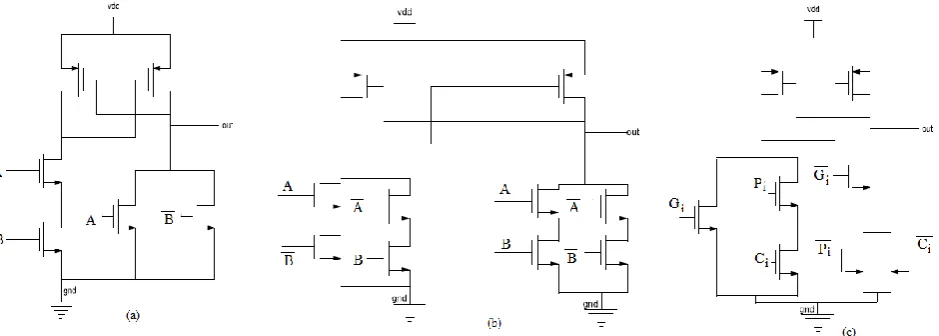
The gates used in the adder are shown in Figure 2 for static CMOS logic.
Fig.2 Static CMOS (a)And gate (b) Xor gate (c) Circuit for Cout
B. ADIABATIC ECRL LOGIC
constant current source instead of a constant voltage source used in conventional CMOS structures. R is the on resistance of pull up PMOS network and C0 is the output capacitance [4].
Fig. 3Equivalent model during charging process in adiabatic circuits
Thus energy dissipation depends upon on resistance R, and it can be minimized by reducing it. Also by increasing the charging time greater than 2RC0 dissipation can be reduced up to large extent. Adiabatic circuits do not utilize standard power supplies as in CMOS circuits; it uses pulsed power supply .
In the Adiabatic logic circuits, the load capacitance is charged through a constant current source instead of a constant voltage source as in case of conventional CMOS circuits [5]. The Adiabatic switching technique is commonly used to minimize the energy loss during the charging and discharging of the load capacitor. In adiabatic circuits, all of the capacitors are charged or discharged at a constant current for the minimization of the power dissipation.
Efficient Charge Recovery logic (ECRL) is One of the most simplest design of the Adiabatic logic where the charge recovery part of the circuit is composed of two cross connected pMOS transistors and the logic portion is made of nMOS transistors. Both the actual logic and the inversion of it can be get from this adiabatic logic circuit
.
The gates used in the adder are shown in Figure 4 for ECRL.
Fig.4 ECRL (a)And gate (b) Xor gate (c) Circuit for Cout
III. RESULT ANALYSIS
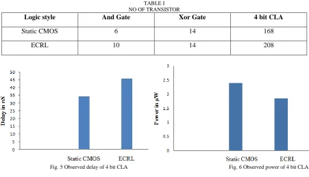
TABLE I NO OF TRANSISTOR
Logic style And Gate Xor Gate 4 bit CLA
Static CMOS 6 14 168
ECRL 10 14 208
Fig. 5 Observed delay of 4 bit CLA Fig. 6 Observed power of 4 bit CLA
IV. CONCLUSION
Adiabatic logic is an efficient technique for designing low power circuits compared to conventional CMOS logic. Simulation indicates it is a power saving logic. From the analysis we can conclude CLA using ECRL logic is a good option for low power circuit design.
REFERENCES
[1] M. Pedram, "Power minimization in IC design: principles and applications," ACM Transactions on Design Automation of Electronic Systems, 1(1): pp 3-56, 1996.
[2] J.Rabey,M.Pendram, “Low power Design Methodologies”,Kluwer Academic Publishers,5th edition. pp 5-7, 2002
[3] S.Kim, Ziesler, C.H.Ziesler and M.C.Papaefthymiou, “Charge-Recovery Computing on Silicon,” IEEE Transactions on Computers, 54, pp. 651-659, 2005.
[4] S.M.Kang, Y.Leblebici,“CMOS Digital Integrated Circuits: Analysis and Design” TATA McGRAW-HILL, 2003.
[5] S. Samanta “Adiabatic Computing” a contemporary review, “4th international conference on computer and devices for communication: codec 09”, 2009.
[6] Guoqiang Hang, ―Adiabatic CMOS Gate and Adiabatic Circuit Design for Low-Power Applications,‖ Design Automation Conference, 2005, pp. 803-808.
[7] K. Takahashi, M. Mizunuma, "Adiabatic Dynamic CMOS Logic Circuit," in Electronics and Communications in Japan Part II, Vol. 83, Issue 5, pp. 50-58, 2000.
[8]Weste, N. and K. Eshraghian, 1993. Principles of CMOS VLSI Design (A Systems Perspective), 2nd Edn., Addison-Wesley, Reading, MA [9] R. Shalem, E. John and L. K. John, “A novel low power energy recovery full adder cell,” in Proc. the IEEE Great Lakes Symp. of VLSI, 1999, pp.380-383..
BIOGRAPHY
Dr. Atanu Nag is working as the Assistant Professor in the Department of Physics, Modern Institute of Engineering &Technology. He has published more than 25 papers in International Journals and attended many conferences.