ISSN(Online): 2320-9801
ISSN (Print): 2320-9798
I
nternational
J
ournal of
I
nnovative
R
esearch in
C
omputer
and
C
ommunication
E
ngineering
(An ISO 3297: 2007 Certified Organization)
Vol. 4, Issue 1, January 2016
High Speed Energy Efficient
Clock-Less Approach for Designing
Asynchronous Architectures
G. Vandana Devi1, Y. E. Vasanth Kumar 2
Assistant Professor, Dept. of E.C.E, Wellfare Institute of Science, Technology & Management,
Visakhapatnam, Andhra Pradesh, India1, 2
ABSTRACT: NULL convention logic is an appealing approach in designing self-timed asynchronous architectures that avoids many problems in standard digital circuits. This technique integrates control and data transformation into a single logical function, yielding a self-timed delay insensitive circuit. This paper presents a novel NCL+ approach supporting Return-to-one protocol (RTO) for designing clock-less digital circuits i.e., delay insensitive asynchronous logic. Comparative analysis have been done among traditional digital CMOS, NCL and NCL+ paradigms to measure the performance and to verify the functionality of each gate using Tanner EDA with 250nm technology in terms of power, propagation delay, power delay product and noise. Simulation results suggest that the proposed NCL+ design consumes less power, offers high speed and more robust to noise.
KEYWORDS: VLSI; CMOS; NCL; NCL+; RTZ; RTO; Threshold Gates.
I. INTRODUCTION
Delay-insensitive self-timed asynchronous circuit design has been the main objective of renewed research for the advantages they provide over traditional synchronous circuit template. Some benefits of these circuits include reduced propagation delay, power consumption, easy design reuse, and less noise [1]. For designing delay insensitive asynchronous design paradigms NULL Convention Logic (NCL) have been proved to be a promising method among various asynchronous design templates. To maintain delay insensitivity NCL circuits employs threshold gates with hysteresis [1, 2]. Several CMOS implementation have been developed for designing NCL gates that includes dynamic, semi-static and static schemes [3-4].
NULL Convention Logic exploits Return-to-Zero (RTZ) handshake protocols, means that all the rails are assigned to zero when there is absence of data in the channel [5, 6]. In this paper, we present a novel approach NCL+ to hold Return-to-One (RTO) [13] protocol, where in the absence of valid data a spacer is provided by assigning all wires to one in the data channel [5-8]. We show that the NCL+ gates offers low power than the NCL and CMOS gates and we also show that the gates produce less noise compared to NCL and CMOS. This paper addresses as, section II describes the overview of NCL. Section III presents the NCL+ design methodology. In Section IV the NCL+ gates are compared with NCL and conventional CMOS gates in terms of average power, propagation delay, power-delay product and noise using Tanner EDA v.15.0 with 250nm technology and conclude in section V.
II. LITERATURE SURVEY
A. NULL Convention Logic:
Delay-Insensitivity, input completeness and hysteresis state holding behavior are the discrete advantages of NCL paradigms [1]. Delay insensitivity signifies that the circuit functions or works correctly despite of when the inputs are obtainable and can be achieved through dual/ quad rail logic [5, 6].
ISSN(Online): 2320-9801
ISSN (Print): 2320-9798
I
nternational
J
ournal of
I
nnovative
R
esearch in
C
omputer
and
C
ommunication
E
ngineering
(An ISO 3297: 2007 Certified Organization)
Vol. 4, Issue 1, January 2016
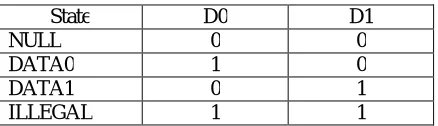
empty set, i.e. no DATA is available. The two rails cannot be asserted simultaneously when they are mutually exclusive, called an illegal state [1, 7, 8].
Table 1: Dual-rail Signal
State D0 D1
NULL 0 0
DATA0 1 0
DATA1 0 1
ILLEGAL 1 1
B. NCL Threshold Gates:
NCL threshold gates with hysteresis ability are constructed to realize the NCL architectures [1, 3]. A fundamental threshold NCL gate, THmn gate is shown in fig. 1, has n inputs and one output. Hysteresis property is imposed by the fact that, after the output is asserted; all the inputs must be de-asserted prior to the output becomes de-asserted [7, 9].
Fig. 1. Fundamental THmn threshold NCL gate
Another type of NCL threshold gate, shown in fig. 2, is the weighted threshold gate, THmnWw1w2…wR, where, m is threshold value and n is number of inputs respectively. The weighted gates have an integer value, m ≥ wR > 1, given
to input R. Here 1 ≤ R < n; where w1, w2 ... wR, are the weights of integer input 1, input 2 ... input R [1, 7].
Fig. 2. Weighted THmnWw1w2…wR NCL gate
To design DI asynchronous architectures, NCL exploits 27 [18-20] fundamental threshold gates. Several CMOS paradigms have been implemented to design NCL architectures, which include dynamic, semi-static and static [3, 9, 10, 11, 12]. Among these the Static implementation of NCL gates, shown in fig. 3, are widely used because of its state holding capacity and are faster than the other two implementations [14-20].
Reset
Set
Hold0
Hold1
Z
Hysteresis property Threshold
property
2 Z
W(R) W(A)
m 1
n
ISSN(Online): 2320-9801
ISSN (Print): 2320-9798
I
nternational
J
ournal of
I
nnovative
R
esearch in
C
omputer
and
C
ommunication
E
ngineering
(An ISO 3297: 2007 Certified Organization)
Vol. 4, Issue 1, January 2016
passed, the receiver acknowledges data by lowering acknowledged signal and to end the logical transition all data wires must return to 1, denoting a spacer [6]. When the spacer is detected the ack signal is raised high, such that a new data transition can begin. These two handshaking protocols from Table 2 supports m-of-n DI codes [6, 8] and can interface with only n inverter stages [13].
Fig. 4. RTO 1-of-2 data transmission
For m-of-n DI codes simplification, RTO (D.x) logical wire can be obtained from RTZ code:
{x ∈N|0 ≤ x ≤m−1} ,
RTO(D. x) =¬RTZ(D. x) eq .(1)
where RTZ (D.x) and RTO (D.x) refers to logical wire values in the RTZ and RTO protocols , respectively. [13].
Table 2: RTO Wire Encoding
Wire Name Spacer Bit ‘0’ Bit ‘1’
D.t 1 1 0
D.f 1 0 1
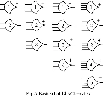
NCL+ is an adaptation of NCL that supports RTO protocol [5]. NCL+ gates can exploit a threshold function with a basic set of 14 NCL+ gates, shown in fig 5. The RTO protocol assigns the logical function of an NCL+ threshold gate to be the reverse of its NCL counterparts [11, 13].
Fig. 5. Basic set of 14 NCL+ gates
The static CMOS implementation of NCL+ threshold gate is shown in fig. 6 that exploits set and reset networks to hold the state information. The basic fundamental difference is that only the wires are inverted/reversed, means that the NCL+ gates assign the switching function to be the inverse of NCL gates.
1
2
1
2
3
1
2
3
4
1
2
3
4
5 +
+
+
+
+
+
+ + + +
+
+
+ + D.t
D.f
ack
1
sp sp sp sp
1 0
ISSN(Online): 2320-9801
ISSN (Print): 2320-9798
I
nternational
J
ournal of
I
nnovative
R
esearch in
C
omputer
and
C
ommunication
E
ngineering
(An ISO 3297: 2007 Certified Organization)
Vol. 4, Issue 1, January 2016
Fig. 6. Static implementation of NCL+ B. NCL+ frame work:
The output will be switched to logic 1, only when all the inputs are encoded to 1. When at least m of its inputs is at logic 0 the output switches to logic0 and keeps the previous value for other combinations of inputs. Both NCL and NCL+ necessitate same number of transistors and are typically equal in terms of cell- topology and area considerations [13].
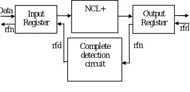
Fig. 7. NCL+ frame work
The NCL+ architecture, shown in fig. 7 consists of two DI registers where the inputs and outputs are configured in mutually exclusive assertion groups. To the input registers, inputs are organized from alternating NULL and DATA wave-fronts. The NCL+ circuit propagates a valid DATA until all the inputs have been received and propagated from the DATA wave-front. Therefore a DATA wave front cannot pass through the NCL+ circuit until all the inputs are DATA or the subsequent register has requested to pass the DATA. After the valid DATA is acknowledged, the output register sends a request for NULL wave front, rfn to the completion circuitry in order detect the completion of DATA wave front. Because of the hysteresis behavior, the gates will not pass NULL until all the inputs have been received and propagated from the NULL wave-front. So when a NULL wave front arrives at the input register, the NULL values will be passed through the output when all the inputs becomes NULL. After the NULL wave front is passed, the completion circuitry detects the NULL and sends a request for DATA; rfd signal to the previous register indicating that it has acknowledged and stored the NULL wave front and the previous register can pass a DATA wave front. Due to completion of NULL and DATA wave-fronts unwanted switching transitions are reduced there by reducing glitching effect.
IV.COMPARATIVE ANALYSIS BETWEEN CMOS, NCL, AND NCL+ PARADIGMS
A. Power Consumption:
Power management is a mounting issue in today’s scenario. Due to switching activity of the active devices the dynamic power is consumed, which is given by the following equation.
CV f
Input Register
Output Register NCL+
Complete detection circuit
rfd rfn
rfd rfn
Data Set
Reset
Hold1
Hold0
Z+
Hysteresis property Threshold
ISSN(Online): 2320-9801
ISSN (Print): 2320-9798
I
nternational
J
ournal of
I
nnovative
R
esearch in
C
omputer
and
C
ommunication
E
ngineering
(An ISO 3297: 2007 Certified Organization)
Vol. 4, Issue 1, January 2016
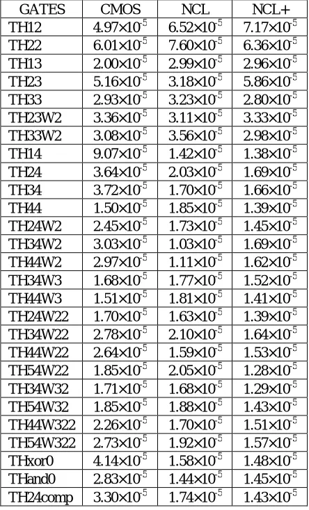
Table 3: Simulation results for average power of CMOS, NCL, NCL+ threshold logic gates (µW)
GATES CMOS NCL NCL+
TH12 4.97×10⁻⁵ 6.52×10⁻⁵ 7.17×10⁻⁵ TH22 6.01×10⁻⁵ 7.60×10⁻⁵ 6.36×10⁻⁵ TH13 2.00×10⁻⁵ 2.99×10⁻⁵ 2.96×10⁻⁵ TH23 5.16×10⁻⁵ 3.18×10⁻⁵ 5.86×10⁻⁵ TH33 2.93×10⁻⁵ 3.23×10⁻⁵ 2.80×10⁻⁵ TH23W2 3.36×10⁻⁵ 3.11×10⁻⁵ 3.33×10⁻⁵ TH33W2 3.08×10⁻⁵ 3.56×10⁻⁵ 2.98×10⁻⁵ TH14 9.07×10⁻⁵ 1.42×10⁻⁵ 1.38×10⁻⁵ TH24 3.64×10⁻⁵ 2.03×10⁻⁵ 1.69×10⁻⁵ TH34 3.72×10⁻⁵ 1.70×10⁻⁵ 1.66×10⁻⁵ TH44 1.50×10⁻⁵ 1.85×10⁻⁵ 1.39×10⁻⁵ TH24W2 2.45×10⁻⁵ 1.73×10⁻⁵ 1.45×10⁻⁵ TH34W2 3.03×10⁻⁵ 1.03×10⁻⁵ 1.69×10⁻⁵ TH44W2 2.97×10⁻⁵ 1.11×10⁻⁵ 1.62×10⁻⁵ TH34W3 1.68×10⁻⁵ 1.77×10⁻⁵ 1.52×10⁻⁵ TH44W3 1.51×10⁻⁵ 1.81×10⁻⁵ 1.41×10⁻⁵ TH24W22 1.70×10⁻⁵ 1.63×10⁻⁵ 1.39×10⁻⁵ TH34W22 2.78×10⁻⁵ 2.10×10⁻⁵ 1.64×10⁻⁵ TH44W22 2.64×10⁻⁵ 1.59×10⁻⁵ 1.53×10⁻⁵ TH54W22 1.85×10⁻⁵ 2.05×10⁻⁵ 1.28×10⁻⁵ TH34W32 1.71×10⁻⁵ 1.68×10⁻⁵ 1.29×10⁻⁵ TH54W32 1.85×10⁻⁵ 1.88×10⁻⁵ 1.43×10⁻⁵ TH44W322 2.26×10⁻⁵ 1.70×10⁻⁵ 1.51×10⁻⁵ TH54W322 2.73×10⁻⁵ 1.92×10⁻⁵ 1.57×10⁻⁵ THxor0 4.14×10⁻⁵ 1.58×10⁻⁵ 1.48×10⁻⁵ THand0 2.83×10⁻⁵ 1.44×10⁻⁵ 1.45×10⁻⁵ TH24comp 3.30×10⁻⁵ 1.74×10⁻⁵ 1.43×10⁻⁵
From the simulation results as shown in table 3, our proposed NCL+ design consumes low power when compared to other conventional CMOS and NCL design models. Therefore the proposed method has an advantage in terms of power consumption.
B. Noise Susceptibility:
In the aspect of noise, our proposed NCL+ design generates less noise when compared to static CMOS and NCL design models. Therefore from the evaluation results shown in table 4, the proposed method has an added advantage in terms noise when compared to CMOS and NCL design styles.
Table 4: Simulation results for noise of CMOS, NCL, NCL+ logic gates
GATES CMOS NCL NCL+
ISSN(Online): 2320-9801
ISSN (Print): 2320-9798
I
nternational
J
ournal of
I
nnovative
R
esearch in
C
omputer
and
C
ommunication
E
ngineering
(An ISO 3297: 2007 Certified Organization)
Vol. 4, Issue 1, January 2016
TH23W2 393.83K 165.51 11.04 TH33W2 196.99K 165.31 31.49 TH14 852.23 524.58 147.20 TH24 31.81K 263.10 37.15 TH34 959.17K 263.01 56.20 TH44 8.10530X 263.05 263.01 TH24W2 51.53K 262.58 27.96 TH34W2 115.81K 263.10 15.17 TH44W2 440.36K 263.08 48.25 TH34W3 715.20K 262.47 8.71 TH44W3 177.12K 263.10 20.51 TH24W22 232.86K 261.62 49.82 TH34W22 46.68K 263.10 12.04 TH44W22 1.23X 263.01 25.08 TH54W22 4.12X 263.04 119.44 TH34W32 78.76K 262.23 14.22 TH54W32 883.64K 263.07 44.08 TH44W322 106.57K 263.10 19.16 TH54W322 970.22K 263.08 61.38 THxor0 597.12K 263.03 32.37 THand0 507.28K 262.97 27.47 TH24comp 597.12K 263.03 32.37
C. Propagation Delay:
To increase the system performance of a digital circuit the propagation delay should be low, which is given by
t = ∝ ( ) eq. (3)
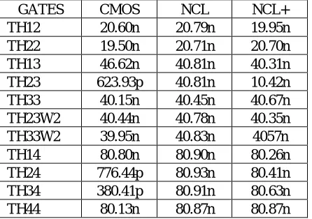
The traditional NCL design consumes more delay than the conventional static CMOS design. In order to reduce the propagation delay of the static NCL gates and improve the performance of the circuit, NCL+ design methodology is used that provides less propagation delay to transmit the valid data and to generates a spacer in the data channel. The simulation values for the three design styles are tabulated in table 5. Based on these simulation results, our proposed NCL+ design show the lowest propagation delay than NCL but the downside is that it produces more delay than the conventional CMOS design.
Table 5: Simulation results of propagation delay for CMOS, NCL, NCL+ gates (s)
GATES CMOS NCL NCL+
ISSN(Online): 2320-9801
ISSN (Print): 2320-9798
I
nternational
J
ournal of
I
nnovative
R
esearch in
C
omputer
and
C
ommunication
E
ngineering
(An ISO 3297: 2007 Certified Organization)
Vol. 4, Issue 1, January 2016
TH24W2 786.59p 80.93n 80.37n TH34W2 40.37n 80.91n 80.54n TH44W2 40.53n 80.90n 80.65n TH34W3 80.61n 80.92n 80.40n TH44W3 80.41n 80.88n 80.63n TH24W22 80.68n 80.93n 80.34n TH34W22 754.54p 80.92n 80.40n TH44W22 419.87p 80.91n 80.59n TH54W22 80.22n 80.86n 80.45n TH34W32 80.64n 80.92n 80.42n TH54W32 79.95n 80.90n 80.65n TH44W322 767.11p 80.92n 80.41n TH54W322 437.29p 80.91n 80.56n THxor0 245.37p 80.91n 80.56n THand0 541.27p 80.92n 80.41n TH24comp 454.20p 80.91n 80.56n D. Power-Delay Product (PDP):
The Power-Delay Product is the product of the total dynamic power and propagation delay, which is given by
PDP = Pdynamic × Tdelay eq. (4)
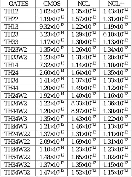
The proposed NCL+ design has finest PDP than the conventional NCL design. The power-delay product for CMOS, NCL and NCL+ gates is tabulated in table 6.
Table 6: Simulation results of power-delay product for CMOS, NCL, NCL+ threshold logic gates (W-s)
GATES CMOS NCL NCL+
ISSN(Online): 2320-9801
ISSN (Print): 2320-9798
I
nternational
J
ournal of
I
nnovative
R
esearch in
C
omputer
and
C
ommunication
E
ngineering
(An ISO 3297: 2007 Certified Organization)
Vol. 4, Issue 1, January 2016
TH44W322 1.73×10⁻¹⁴ 1.37×10⁻¹² 1.21×10⁻¹² TH54W322 1.19×10⁻¹⁶ 1.55×10⁻¹² 1.26×10⁻¹² THxor0 1.01×10⁻¹⁵ 1.26×10⁻¹² 1.19×10⁻¹² THand0 1.53×10⁻¹⁴ 1.16×10⁻¹² 1.16×10⁻¹² TH24comp 1.49×10⁻¹⁴ 1.40×10⁻¹² 1.15×10⁻¹²
V. CONCLUSION AND FUTURE WORK
In this work, we have designed and implemented delay-insensitive asynchronous static NCL+ library. All the static NCL+ gates were configured, successfully simulated and verified to be functionally correct. Furthermore power, propagation delay, power-delay product and noise of each gate is simulated and calculated. From the simulation results it is observed that power consumed and by each gate is less when compared with static NCL and CMOS topologies and the proposed design is more robust to noise, which is an added advantage. NCL+ provides less delay and power-delay product compared to NCL but the drawback is that it provides more delay when compared to static CMOS design. Future work includes optimizing the propagation delay for higher performance and better speed of operation.
REFERENCES
1. S.C. Smith and J. Di, “Designing asynchronous circuits using NULL Convention Logic (NCL),” Synthesis Lectures on Digital Circuits
and Systems: Morgan & Claypool Publishers, 2009.
2. M. Ligthart, K. Fant, R. Smith, A. Taubin, and A. Kondratyev, “Asynchronous design using commercial HDL synthesis tools,” in
Advanced Research in Asynchronous Circ. and Syst., Proc. Sixth Int. Symp. on, Apr.2000, pp. 114–125.
3. G.E. Sobelman, and K.Fant, “CMOS circuit design of threshold gates with hysteresis,” in Circ. and Syst., Proc. Of the IEEE Int. Symp.
on, Jun. 1998, pp.61–64.
4. M. Shams, J.C. Ebergen, and M.I. Elmasry, “Modeling and comparing CMOS implementations of the C-element,” Very Large Scale
Integ. (VLSI) Syst., IEEE Trans. on, vol. 6, no. 4, pp. 563–567, Dec.1998.
5. Matheus T. Moreira, Ney L. V. Calazans, “Quasi-Delay-Insensitive Return-to-One Design”, 2014.
6. A. Martin, .The Limitations to Delay-lnsensitivity in Asynchronous Circuits,. Advanced Research in VLSI: Proceedings of the Sixth MIT
Conference: pp. 263-278, 1990.
7. Karl M. Fant and Scott A. Brandt, .NULL Convention Logic: A Complete and Consistent Logic for Asynchronous Digital Circuit
Synthesis,. International Conference on Application Specific Systems, Architectures, and Processors, pp. 261-273, 1996.
8. T. Verhoff,. Delay-Insensitive Codes. An Overview,. Distributed Computing, Vol. 3, pp. 1-8, 1988.
9. Farhad A. Parsan and Scott C. Smith, “CMOS Implementation of Static Threshold Gates with Hysteresis: A New Approach”, IEEE/IFIP
Int. Conf. on VLSI and System-on_Chip (VLSI-SoC), Oct. 2012.
10. Farhad. A. Parsan and Scott. C. Smith, “CMOS Implementation Comparison of NCL Gates,” IEEE Int. Midwest Sym. on Circuits and
Systems (MWSCAS), Aug. 2012.
11. S. Yancey, and S. C. Smith, “A differential design for C-elements and NCL gates,” in Circ. and Syst., 53rd IEEE Int. Midwest Symp. on,
Aug. 2010.
12. Harish Gopalakrishnan, “Energy Reduction for Asynchronous Circuits in Soc Applications”, Dissertation, 2005.
13. Matheus T. Moreira, Carlos H. M. Oliveira, Ricardo C. Porto, Ney L. V. Calazans, “NCL+: Return-to-One Null Convention Logic”,
Circuits and Systems (MWSCAS), Aug 2013.
14. B. Bhaskaran, V. Satagopan, and S. C. Smith, “High-Speed Energy Estimation for Delay-Insensitive Circuits,” The 2005 International
Conference on Computer Design, June 2005.
15. Scott Christopher Smith, “Gate and Throughput Optimizations for Null Convention Self-Timed Digital Circuits”, Dissertation, 2001.
16. V. Satagopan, B. Bhaskaran, A. Singh, and S. C. Smith, “Energy Calculation and Estimation for Delay-Insensitive Digital Circuits,”
Elsevier’s Microelectronics Journal, Vol. 38/10-11, October/November 2007.
17. P. A. Beerel, R. O. Ozdag and M. Ferretti, “A Designer’s Guide to Asynchronous VLSI”, Cambridge University Press, 2010.
18. S. C. Smith, R. F. DeMara, J. S. Yuan, D. Ferguson, and D. Lamb, “Optimization of NULL Convention Self-Timed Circuits,” Elsevier's
Integration, the VLSI Journal, Vol. 37/3, August 2004.
19. B. Bhaskaran, V. Satagopan, W. Al-Assadi, and S. C. Smith, “Implementation of Design For Test for Asynchronous NCL Designs,” The