ABSTRACT
NOZARIASBMARZ, AMIN. In-situ Sintering Decrystallization of Thermoelectric Materials using Microwave Radiation (Under the direction of Dr. Daryoosh Vashaee).
Thermoelectric materials are capable to convert heat directly into electricity. Today with nearly 60% of the useful energy wasted as heat, thermoelectric materials are expected to play an important role is recovering significant amount of wasted heat helping to reduce consumption of fossil fuels and to reduce the greenhouse gas emissions. The efforts in developing good thermoelectric materials have followed mainly two directions. The first approach has been finding new bulk materials and further engineering them to increase their dimensionless thermoelectric figure-of-merit, zT. The second approach has been the nanostructuring approach that reduces the thermal conductivity through scattering of phonons at interfaces. In some cases, nanostructuring has also improved the power factor (S2) through interface energy filtering.
The latter approach based on reducing the thermal conductivity has resulted in numerous high zT thermoelectric materials. The smallest thermal conductivity can be achieved in an amorphous material where the density of defects is so high that neither long range nor short range order of the atoms exist. Amorphous phases can possess fundamentally different electrical and thermal properties than crystalline or nano-crystalline forms of the thermoelectric materials. The interfaces in amorphous materials introduce sites for scattering of both charge carriers and phonons; therefore, a fully amorphous material is unlikely to make a good thermoelectric material due to poor electrical conductivity. However, a composite material consisting of mixed amorphous and crystalline phases can be engineered to reduce the thermal conductivity more than the electrical conductivity. There has been only limited work on bulk amorphous electronic materials, and even less on their thermoelectric properties. This is mainly due to the challenges in making large size bulk amorphous materials, which has discouraged their large scale applications.
This method is especially interesting as it is extendable to different materials. Many thermoelectric materials can be sintered and decrystallized with this approach. Furthermore, materials in different forms and structures like powder, cold pressed, hot pressed, solidified from the melt, single crystalline, polycrystalline, nanocrystalline, or nanocomposites can be processed in this method.
The other part of this dissertation focuses on the application of microwave radiation on two different materials for specific applications at room temperature and at high temperature. P-type (Bi,Sb)2Te3 and n-P-type Bi2(Se,Te)3 amorphous-crystalline structures were developed for body heat harvesting applications. Body heat harvesting thermoelectric generators (TEG) can play a key role in future healthcare electronic devices. These devices can steadily generate electricity from body heat to power wearable or implantable medical, health, and sport devices. A TEG that can work efficiently in a wearable platform must be optimized both at material, device, and system level. At materials level, the dimensionless thermoelectric figure-of-merit, zT, is not the only important property and low thermal conductivity is also required. Low thermal conductivity is necessary due to the large thermal resistance of the skin and poor heat rejection condition at the cold side of the TEG. For efficient operation at system level, the material must also have a high Seebeck coefficient to generate useful voltage for efficient operation of the subsequent DC/DC boost convertor. The (Bi,Sb)2Te3 and Bi2(Se,Te)3 amorphous-crystalline composites were especially engineered to meet the requirements for self-powered wearable applications.
For high temperature applications, such as waste heat recovery or power generation at industrial processes, improving zT is the most important factor to improve the efficiency of the thermoelectric materials. It was shown that the microwave processing of Si0.80Ge0.20 can lead to a unique composite structure with desired compositional variations among the grains. This resulted in synthesizing Si1-xGex alloy with 0.5≤x≤0.9. In addition, the microwave processing resulted in a microstructure with large intra grain dislocation density which was dispersed throughout the material. This resulted in simultaneous reduction of the thermal conductivity and increase of the thermoelectric power factor of SiGe alloy, which is often difficult to achieve.
In-situ Sintering Decrystallization of Thermoelectric Materials Using Microwave Radiation
by
Amin Nozariasbmarz
A dissertation submitted to the Graduate Faculty of North Carolina State University
in partial fulfilment of the requirement for the degree of
Doctor of Philosophy
Electrical Engineering
Raleigh, North Carolina 2017
APPROVED BY:
_______________________________ ______________________________ Dr. Mehmet C. Öztürk Dr. Veena Misra
_______________________________ ______________________________ Dr. James M. LeBeau Dr. Daryoosh Vashaee
ii
DEDICATION
iii
BIOGRAPHY
Amin Nozariasbmarz received his Bachelors of Science in Materials Science and Engineering from Sharif University of Technology in 2008 and his Master of Science in Materials Science and Engineering from University of Tehran in 2011. He joined ECE Department at North Carolina State University in January 2015 as PhD student after studying for two years at Oklahoma State University. He also completed a minor degree in Materials Science and Engineering at NC State University. Since 2013, his research has been focused on thermoelectric materials under the supervision of Dr. Daryoosh Vashaee.
Amin’s main research is on fabrication and characterization of nanostructured and decrystallized thermoelectric materials, particularly on p- and n-type SiGe alloys and their nanocomposites for high temperature power generation applications, and p- and n-type bismuth telluride alloys for body heat harvesting. He has published over 20 papers in peer-reviewed scientific journals and presented fifteen conference articles.
iv
ACKNOWLEDGMENTS
First, I would like to thank again my parents and my wife. They had a hard time not visiting me during my PhD studies but they supported and encouraged me to reach my whole-life goal. Throughout my entire life my parents have been always supportive with any path I have chosen. Without my father’s guidance and my mother’s love I would not have been able to reach my goals and for that I am truly thankful. I would like to wholeheartedly appreciate my dear wife, Aysel, for her unconditional and unlimited support for my carrier during all these years that we had to live separated from each other.
I would like to thank Airforce Office of Scientific Research and National Science Foundation who funded my research. In addition, I would like to truly thank Helmerch Advanced Technology Research Center at Oklahoma State University and the ASSIST Engineering Research Center at North Carolina State University (NCSU) for supporting this project and giving me the opportunities needed for my work. I would like to thank the Analytical Instrumentation Facility (AIF) at NCSU and its staff Ching-Chang Chung, Chuck Mooney, Yang Liu and Toby Tung for their training and characterization help. I would like to also appreciate staff of the NCSU Nanofabrication Facility (NNF) especially Nicole Hedges, Marcio Cerullo and Henry Taylor for all their help.
I would like to especially thank Dr. Jerzy S. Krasinski at Oklahoma State University for his invaluable suggestions and comments during my PhD. I would like to personally thank each of my committee members for their help on this work; Dr. Mehmet C. Öztürk for his fatherly advices and additional guidance for my research; Dr. Veena Misra for her endless energy to fulfill the ASSIST’s goals and perfectly manage the projects; Dr. James M. LeBeau for his expertise and unconditional support of my work by using transmission electron microscopy. I want to also express gratitude for Dr. Lobat Tayebi for her kind support and the students and friends that have helped and supported me through all of this work including Dr. Payam Norouzzadeh, Milad Mohebali, Pouya Amrollahi, Dr. Zahra Zamanipour, Dr. Nikhil Satyala, Dr. Iurii Kogut, Zachary Carpenter, Abhishek Malhorta, Michael J. Hall, Aditi Agarwal, Zachary A. Coutant, Christopher Boggs, Jie Liu, Runze Liu, Haywood Hunter, Nicholas Snouwaert, Dr. Francisco Suarez, Matthew J. Cabral, and J. Houston Dycus.
v
TABLE OF CONTENTS
LIST OF TABLES ………. x
LIST OF FIGURES ……….. xi
CHAPTER 1: Introduction ... 1
1.1 Good Thermoelectric Materials ...2
1.2 Efficiency of Thermoelectric Materials ...3
1.3 Classical Approach ...4
1.4 Recent Prospective ...6
1.4.1 Nanostructured Thermoelectric ...6
1.4.2 Nanocomposite Approach ...8
1.5 Future Prospective: Amorphous/Decrystallized and Amorphous-Crystalline Thermoelectrics ...9
CHAPTER 2: Transport Properties Measurement and Characterization of Thermoelectric Materials ... 12
2.1 Mechanical Milling/Alloying/Mixing ...12
2.2 Introduction Melting ...13
2.3 Hot Pressing ...14
2.4 Microwave Processing ...15
2.5 Scanning Electron Microscopy ...16
2.6 Transmission Electron Microscopy ...17
2.7 X-ray Diffraction ...17
2.8 Electrical Conductivity and Seebeck Coefficient Measurement ...17
2.9 Thermal Conductivity Measurement ...19
CHAPTER 3: Fundamentals of Microwave Processing ... 22
3.1 Introduction ...22
3.2 Microwave Processing of Thermoelectric Materials ...23
3.3 Basic Components of Microwave Setup ...24
3.3.1 Magnetron...25
vi
3.3.3 Circulator/Isolator...28
3.3.4 E-H Tuner ...28
3.3.5 E-H Tuner ...29
3.3.6 Applicator ...29
3.3.7 Sliding Short or Plunger ...29
3.3.8 Monitoring systems ...29
3.3.8.1 Temperature monitoring system... 29
3.3.8.2 Microwave Monitoring System ... 30
3.4 Basic Concepts in Microwave Processing ...30
3.4.1 Interaction of Materials with Microwave ...30
3.4.2 Dielectric Heating ...31
3.4.3 Non-uniform Heating ...37
3.4.4 Thermal Runaway ...38
3.4.5 Plasma...38
3.4.6 Electric Discharge ...39
3.5 Conclusions ...39
CHAPTER 4: Microwave Processing of Thermoelectric Materials ... 40
4.1 Introduction ...40
4.2 Experimental Procedure ...42
4.2.1 Materials Processing ...43
4.2.2 Microwave Processing...44
4.2.3 Characterization ...45
4.3 Results and Discussion ...45
4.3.1 Microwave Processing of the Materials ...45
4.3.2 Amorphous Structure...49
4.3.3 Amorphization and Decrystallization ...52
4.3.4 Microwave Processing of Bi2Te3 and Sb2Te3 Powders ...53
4.3.5 Microwave Processing of SiGe ...57
vii
4.4 Conclusions ...61
CHAPTER 5: Effect of Microwave Processing on Bismuth Antimony Telluride Alloys……… ... 63
5.1 Introduction ...63
5.2 Experimental Procedure ...65
5.3 Microwave processing of Bismuth Antimony Telluride ...67
5.4 Microwave Processing Below 400 °C ...67
5.5 Microwave Processing Above 400 °C ...71
5.6 Effect of Glass Inclusion ...76
5.7 Effect of Annealing ...79
5.8 Conclusions ...86
CHAPTER 6: P-type (Bi,Sb)2Te3 Nanocomposites for Body Heat Harvesting ... 88
6.1 Introduction ...88
6.2 Design and Optimization of the TEG Parameters ...90
6.2.1 TEG on Body ...90
6.2.2 Parasitic Resistance ...91
6.2.3 Material Optimization ...92
6.3 Experimental Procedure ...94
6.3.1. Material Synthesis ...94
6.3.2. Materials Characterization ...96
6.3.3. Thermoelectric Property Measurement ...96
6.4 Results and Discussion ...96
6.4.1. (BixSb1-x)2Te3 Nanocomposites ...96
6.4.2. Engineering the Thermal Conductivity ...98
6.4.3. Microstructure ...98
6.4.4. Transport Properties ...99
6.4.5. Experimental Results Versus Model ...103
viii
CHAPTER 7: N-type Bi2(Se,Te)3 Nanocomposites Optimized for Body Heat
Harvesting ..…… ... 107
7.1 Introduction ...107
7.2 Experimental Procedure ...109
7.2.1 Material Synthesis ...109
7.2.2 Material Characterization ...111
7.2.3 Thermoelectric property measurement ...111
7.3 Results and Discussion ...112
7.3.1 Effect of Dopant Addition ...115
7.3.2 Optimizing Te Vacancy ...116
7.3.3 Effect of Soaking Time ...118
7.3.4 Effect of Glass Inclusion ...120
7.3.5 Microwave Assisted Processing ...121
7.3.6 Effect of Microwave Processing with Glass Inclusion...125
7.3.7 Effect of Initial Hot Press Temperature...127
7.3.8 Effect of Annealing ...130
7.3.9 Comparison with the State-of-the-art Data ...131
7.4 Conclusions ...132
CHAPTER 8: Microwave Processed P-Type Si0.8Ge0.2 with Enhanced Thermoelectric Properties ……… ... 134
8.1 Introduction ...134
8.2 Experimental Procedure ...136
8.3 Results and Discussion ...139
8.3.1 Optimization of Sintering ...139
8.3.2 X-ray Diffraction Pattern ...139
8.3.3 Microstructure ...140
8.3.4 Uniformity of the Microwave Processed SiGe Samples ...143
8.3.5 Transport Properties ...144
ix
x
LIST OF TABLES
Table 4-1- List of composition and synthesis parameters of raw materials prior to exposure to
microwave energy ... 43
Table 5-1- Sintering parameters of processed samples ... 68
Table 5-2- Sintering parameters of processed samples above 400 °C ... 72
Table 5-3- Properties of different Ferro glasses ... 76
Table 5-4- Sintering parameters of processed samples ... 81
Table 6-1- Composition, sintering parameters, room temperature thermal conductivity and ZT of selected synthesized nanocomposites ... 95
Table 7-1: List of composition, synthesis parameter, room temperature Seebeck, thermal conductivity, zT and maximum zT of the synthesized materials... 112
xi
LIST OF FIGURES
xii Figure 2-5- ZEM-3 Ulvac setup for measuring electrical conductivity and Seebeck coefficient.
... 19
Figure 2-6- (a) Netzsch's LFA 457 Micro Flash equipment for thermal diffusivity measurement, (b) schematic cross section of the equipment. ... 20
Figure 3-1- Schematic drawing of the conventional heating versus microwave heating. ... 22
Figure 3-2- Schematic image of microwave setup and the position of the sample. ... 25
Figure 3-3- Magnetron and its cross section [104]. ... 27
Figure 3-4- Schematic representation of the microwave interaction and a diatomic molecule resulting in torque and rotation on the molecule. ... 31
Figure 3-5: Frequency dependency of ε′ and ε″ []. The microwave frequencies are highlighted and the frequency range of the microwave used in this study (2.54 GHz) is shown by a red dashed line. ... 35
Figure 3-6: ε′ and ε″ calculated as a function of ωτ based of Debye expression [115,116]. .. 35
Figure 3-7: Schematic diagram of the temperature dependency of dielectric constant [119]. 36 Figure 3-8- Temperature dependence of Tan δ for Glass, Al2O3, SiO2 and Al2O3 [98]. ... 37
Figure 4-1- Schematic illustration of a microwave system. ... 48
xvii Figure 6-7: Generated power versus thermal conductivity for different zT values of synthesized nanocomposites. Solid lines are the data generated from the model and the red dots are the actual developed experimental data from this work. The model was generated for a device with p-type nanocomposite legs and n-type commercial legs. ... 104 Figure 6-8: Generated power versus zT for different thermal conductivity values of synthesized nanocomposites. Solid lines are the data generated from the model and the red dots are the actual developed experimental data for the nanocomposite p-type and commercial n-type. The red dots on the model data for the nanocomposite n- and p-type is hypothetical experimental data. ... 105 Figure 7-1- Schematic view of the microwave setup. The sample sits at the center of the waveguide where there is the maximum electric field. ... 113 Figure 7-2- (a) Comparison of the XRD patterns of pure Bi2Te3 powder with the microwave processed one; the intensity is in arbitrary unit (a.u.), (b) Enlarged XRD patterns around
1
CHAPTER 1:
Introduction
According to the International Energy Outlook 2016, the energy demands are expected to increase over the next 30 years and the total energy consumption is expected to go up by 48% from 2012 to 2040 [1]. This will naturally lead to an increase in the greenhouse effect and the global warming and therefore, the need for sources of renewable energy is more pressing now than ever.
Today more than 60% of the energy is wasted as heat. Therefore, means to generate useful energy from heat can help saving huge amount of energy. One of the most promising technologies to recover waste heat from industries and vehicles is based on thermoelectric effect in which the temperature difference is directly converted to voltage and vice versa. The thermoelectric phenomenon has been understood well since the old discoveries by Seebeck in 1821, Peltier in 1834, and Thomson in 1851. The unique advantages of the thermoelectric materials compared to the other technologies include consistent conversion of heat to electricity and vice versa, no mechanical movement, lack of chemical waste and noise pollution, sustainability and environmental friendliness along with the user safety and friendliness [2,3,4].
The quality of a thermoelectric material is determined by the thermoelectric dimensionless figure-of-merit, zT, specified by Equation 1-1:
zT = S σ
κ T (1-1)
2 According to the zT formula, the main challenge in the field of thermoelectric materials is that the thermal conductivity opposes the electrical conductivity and Seebeck coefficient. In other words, by rearranging Equation 1-1, zT=(S2n)(μ/κ)eT. The components in the two parenthesis have contradictory properties [6]. According to Pisarenko relation [7], higher n results in lower S. Besides, defects reduce both κ and μ. Therefore, there is always a compromise among these properties.
It should also be considered that due to the limitations of the measurement instruments commercially available today, the reported zT in the literature can have on the average 20% tolerance [8]. Besides, improper sample geometries can also increase the tolerance. Therefore, small zT improvements may be within the measurement variation. In addition, considering only the maximum zT as the only criteria for determining thermoelectric material’s excellency is not accurate because the thermoelectric leg might encounter a broad temperature differential during the application. Therefore, thermoelectric materials with high zT over a broad range of temperature are desired [9].
Nowadays, the applications of thermoelectric materials are growing in different areas and sooner or later along with the high zT, their availability, sustainability, environmental friendliness, cost, recyclability, thermal stability, chemical and mechanical properties should be also taken into account.
1.1
Good Thermoelectric Materials
3 [19]. Another direction is the use of nanostructures (e.g. superlattices) that improve the power factor (S2) through quantum size effects [20,21,22], or interface energy filtering [23,24,25], while their thermal conductivity is reduced through scattering of phonons at interfaces [21,26]. Some examples of these groups include ErAs rare earth nanocomposites and ScN/ZrWN multilayers for thermoelectric energy conversion [27,28,29,30]. The improved zT in these structures comes mainly from the reduction in phonon thermal conductivity and to a lesser extent, from enhancing the power factor. Nanostructured bulk Bi2Te3 [31,32,33] and PbTe [34] based materials showed high zT resulted from the presence of nano-domains [35].
Figure 1-1- The state-of-the-art reported zTs versus temperature.
1.2
Efficiency of Thermoelectric Materials
4 Figure 1-2- Schematic corner and side view of a thermoelectric device showing p- and n- type legs.
The thermoelectric conversion efficiency (η) can be calculated using Equation 1-2 [36]:
η = T − T T
(1 + ZT) − 1
(1 + ZT) + TT (1-2)
where TH and TC are the temperatures of the hot and the cold side, respectively. The term (TH -TC)/TH is the Carnot efficiency, which is the maximum efficiency for a reversible cycle. We use zT (with lower case z) to represent material’s and ZT (with upper case Z) for the device’s thermoelectric dimensionless figure of merit [37]. ZT is usually less than zT due to parasitic effects such as heat losses, Joule heating at the metal contacts and interconnects, or the non-uniformity of the zT along the material [38]. A high peak zT does not necessarily produce an efficient device. At device level, a high zT at the working temperature and also along the material from the hot to cold side is necessary to achieve a high efficiency.
1.3
Classical Approach
5 (GaP) particles in SiGe host alloy by Pisharody in 1978 [39]. This resulted in 40-50% reduction of thermal conductivity in both n- and p-type materials; hence, higher zT for SiGe alloy was obtained. Another influential work was performed by Rowe [40] in 1974 known as fine grain SiGe in which they came up with the idea of using grain boundary scattering of phonons to reduce the thermal conductivity [41,42,43]. This work opened a roadmap for the future works on SiGe [44].
Theoretically, there is no limit for maximum zT; however, for several decades the maximum zT for the state-of-the-art thermoelectric materials, i.e. SiGe, PbTe and (Bi,Sb)2Te3, remained near unity [2]. To make thermoelectric devices comparable to the current technologies such as combustion of fossil fuels zT>3 is required [2,45,46]. Furthermore, thermoelectric materials should be inexpensive, robust, non-hazardous and environmental friendly for applications such as in vehicle industries. Historically different methodologies have been used to improve the zT such as using heavy element compounds, complex crystal structures, point defect scattering, and use of dopants with resonant states near the band edges [46].
6
1.4
Recent Prospective
1.4.1 Nanostructured Thermoelectric
Since early 1990s, two approaches have been taken to initiate the next generation of thermoelectric materials. One is using the new class of advanced bulk thermoelectric materials [54,55] and the other is using low-dimensional thermoelectric materials also called nanostructuring [20,56].
The advanced bulk thermoelectric materials are based on the fact that one of the lowest thermal conductivities has been obtained in glasses. In fact, instead of fast transport through phonons, the thermal conductivity of glasses is a random walk of energy over the lattice. However, due to the absence of electron-crystal properties, low mobility and effective mass, glasses are not considered as thermoelectrics. For a good thermoelectric material, unique properties are needed, i.e. a crystalline material with good electron mobility but high scattering for phonons [36]. The term “phonon-glass electron-crystal” (PGEC) was coined to define materials that would allow the movement of charge carriers, like crystalline semiconductors, however, highly restrict the phonon heat transport as in glasses [57,58]. These materials should have extremely small thermal conductivity while maintaining a relatively large power factor [59]. Materials such as skutterudite and clathrates with large caged like unit cells and a guest atom trapped inside the cage, known as the rattler, were largely investigated as candidates to achieve PGEC properties (for more information see reference [57]). On another direction, recently, zT=2.6 was achieved in a single crystal of SnSe with PGEC characteristics [19]. This result showed that that PGEC characteristics are not limited to the structures with rattling atoms.
7 phonons more than electrons and as a result, in nanostructured thermoelectric materials, the thermal conductivity reduces more than electrical conductivity.
There were several successes in achieving enhanced zT in nanostructured n-type and p-type SiGe [60,61,62] although nanostructuring did not show significant enhancement in zT of other silicide alloys such as MnSi1.7 [63], Mg2Si [64,65], and FeSi2 [66,67].
Figure 1-3-a shows the transmission electron microscopy image of a nanostructured bulk Bi0.5Sb1.5Te3 alloy synthesized via mechanical alloying and hot pressing. The experimental result showed that zT of the nanostructured alloy was enhanced (Figure 1-3-b) due to the reduction of lattice thermal conductivity as a result of scattering of phonons at grain boundaries and defects [31].
Figure 1-3- (a) High resolution transmission electron microscopy image of a hot pressed Bi0.5Sb1.5Te3 and (b) comparison of the zT of nano-grained and micro-grained (Bi,Sb)2Te3 alloy [31].
8 interfaces and grain boundaries along with precipitates and point defects. Consequently, due to the wide distribution of the defect sizes in the nanostructured materials, phonon scattering can be effective both for short and long wavelengths [53].
It should be considered that nanostructured thermoelectrics are generally highly doped to compensate for the loss of electrical conductivity. In addition, because of the preferential scattering of low energy (long wavelength) charged carriers at interfaces, the Seebeck coefficient in nanostructured thermoelectric materials can also improve [68].
1.4.2 Nanocomposite Approach
The term “nanocomposite” is designated to a broad class of materials, however it is generally used to refer to the materials which contain nano-grains and nano-features along with structural defects. Nanocomposites can have lower thermal conductivity than the “alloy limit” [27]. High zT has been obtained in several thermoelectric nanocomposites such as InGaAs/ErAs [27,69], PbTe-SrTe [34,70], SiGe-CrSi2 [71], and (Bi,Sb)2Te3 [72]. In another study, Mingo et al. predicted enhanced zT in nanocomposites made of silicide nanoparticles in SiGe alloy [73]. Experimental values further confirmed this prediction [74,75].
In nanocomposite approach, the thermoelectric materials are fabricated by compacting nanoparticles. Nanocomposites are isotropic and they have lower thermal conductivity, higher power factor and improved mechanical properties rather than a single crystal or large grain crystal of the same materials [76]. Figure 1-4 shows a schematic of probable microstructure for different types of thermoelectric nanocomposites.
9
Figure 1-4- Different types of nanocomposite structures. (a) Nanoparticles (nanoinclusion) or
defects in alloy, (b) Nano-grain, (c) Nanocomposite with compositional gradients in different grains, and (d) Amorphous-crystalline nanocomposite. It should be considered that each grain can consist of several defects such as twin boundaries, interfaces and dislocations that also make several sub-grains inside a grain.
1.5
Future Prospective: Amorphous/Decrystallized and Amorphous-Crystalline
Thermoelectrics
10 most likely be close to the band edges. The localized states in crystalline materials are discrete levels in the form of Dirac delta function; however, amorphous materials have continuous band of energy levels [78].
Basically, amorphous phases have different transport properties compared to crystalline and/or nanocrystalline thermoelectric materials [79]. Due to the challenges of their fabrication, there has been restricted research on fabricating bulk amorphous electronic materials, specifically in the field of thermoelectric materials.
zT in fine grained and amorphous thermoelectric materials was conceptually calculated by Nolas and Goldsmid in 2002 [80]. They showed that under some conditions, amorphous materials should have high zT compared to the crystalline ones. Nevertheless, there are only limited reports on fabrication of bulk amorphous thermoelectric materials [81]. The concept of amorphous-crystalline thermoelectric materials is a promising approach to achieving high performance thermoelectric materials. These materials have characteristics similar to PGEC concept.
High Seebeck coefficient can be achieved either by designing the density of states via electronic structure modification [18,82] or manipulating nanostructures [83]. Amorphous thermoelectric materials have low thermal conductivity while their functionality is restricted because of their small electrical conductivity. A new structure based on amorphous-crystalline phase can provide possibilities to reduce the thermal conductivity more than the electrical conductivity and enable making good thermoelectric materials.
12
CHAPTER 2:
Transport Properties Measurement and
Characterization of Thermoelectric Materials
In this chapter, the fabrication methods, measurement of transport properties and characterization of the synthesized thermoelectric materials will be discussed. The details of synthesis process and characterization techniques will be explained in further chapters.
2.1
Mechanical Milling/Alloying/Mixing
High purity powders were weighed in stoichiometric ratio and loaded in tungsten carbide (WC) bowl. Depending on the powder and milling/alloying condition WC balls were added to the bowl with a certain ball to powder (BPR) ratio. The milling parameters are the milling time (i.e. the total running time), the ball to powder ratio (BPR), and the milling speed (up to 1000 rpm). The milling parameters were optimized for each material separately. The bowl was sealed inside an argon filled glove box. The powders were milled/mixed using Fritsch-P7PL and Fritsch-P6 planetary ball mills. The mechanical alloying and milling process were explained in detail by Suryanarayana [84]. More information about the milling parameters will be explained in detail in the following chapters.
13 Figure 2-1- (a) Fritsch-P7PL planetary ball mill with WC bowls and balls, and (b) Thinky mixer and its cup.
2.2
Introduction Melting
Introduction furnace uses principle of induction to heat materials up to their melting temperature. The high frequency magnetic field helps to stir the molten material to make a uniform alloy. The induction heating process uses electromagnetic induction to heat an electrically conductive material due to heat created in the material by the eddy current. The induction furnace consists of a water-cooled copper coil surrounding a refractory material like quartz. The process results in a clean uniform alloy. The material can be placed in a sealed chamber with controlled atmosphere and the chamber is subjected to induction heating. For example, in this research, graphite crucible was used as electrically conductive material and the mixture of the powders was placed in the crucible. Then, the crucible was loaded in a quartz tube (chamber) and sealed inside the glovebox to protect the material from oxidation. Finally, the system is subjected to induction melting.
14 In this research, Bi2Te3 and Sb2Te3 alloys were prepared via induction melting. Stoichiometric ratio of high purity elements of Bi powder/Te lump, and Sb powder/Te lump were separately mixed and melted in induction furnace to prepare homogenized Bi2Te3 and Sb2Te3 ingots. 2% excess Te was added to the mixture to compensate for Te loss during induction melting. The process was carried out in a graphite die inside a quartz tube under argon atmosphere. (Bi,Sb)2Te3 alloy was also prepared with this method. Figure 2-2-a and b shows the induction melting system and Bi2Te3 ingot made from induction melting. Finally, the ingots were milled by planetary ball mill to obtain a uniform mixture of nanostructured powder.
Figure 2-2- (a) Induction melting process, and (b) Bi2Te3 ingot made from induction melting.
2.3
Hot Pressing
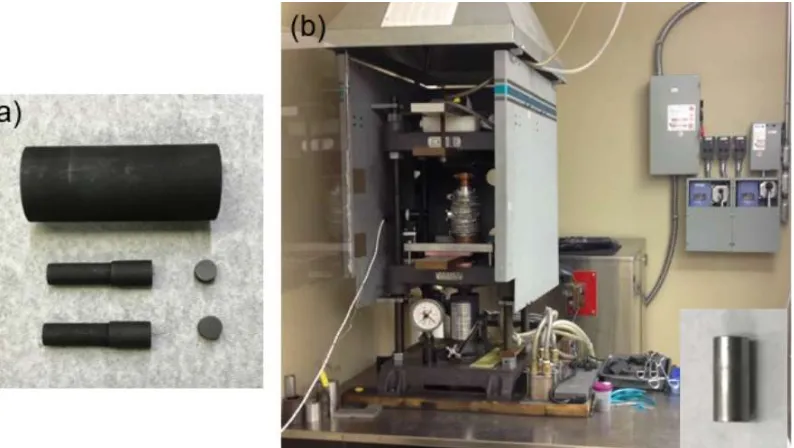
A custom made P2C hot press system was used to densify and sinter the nanostructured powders. The milled powders were collected and loaded into a graphite die with internal diameter of 6 mm. The powder was pressed inside the graphite rod. Two spacers were placed on the bottom and the top of the powder followed by graphite rods to press the sample. The spacers were used to protect the rods from sticking to the hot pressed samples.
15 thermocouple sitting at the center of the graphite die containing the sample. The die was placed in a controlled-atmosphere chamber to protect the sample from oxidation while sintering. The die is heated up by passing a direct current (DC) through the sample. The required pressure was applied on the sample by a hydraulic press.
Figure 2-3-b shows the custom made hot pressing system. The main sintering parameters are the sintering temperature, soaking time and pressure. For each material system, the sintering parameters were experimentally optimized. The higher the temperature and holding time, the larger the grain size. The synthesized samples had a diameter of 6 mm, which provides the option to measure the transport properties in the same direction.
Figure 2-3- (a) Graphite die, rods and spacers used for hot pressing, and (b) the custom made hot pressing system with atmosphere controlled chamber. The inset shows the sintered cylindrical rod made by hot pressing.
2.4Microwave Processing
16 during the exposure of the samples. The temperature profile was monitored using a pyrometer sensor facing the sample. The experiments were conducted in an inert atmosphere by loading the samples into a boron nitride (BN) crucible and then hermetically sealing the crucible inside a quartz tube. The quartz tube was then deoxidized using a vacuum pump and filled with inert gas. The process was repeated multiple times. N2 and Ar were used to provide inert atmosphere. The pressure of the gas was maintained at 700 torr inside the quartz tube during the experiments. The exposure time varied for different samples. It ranged from a few seconds for Bi2Te3 and Sb2Te3 powders to more than 10 minutes for SiGe samples.
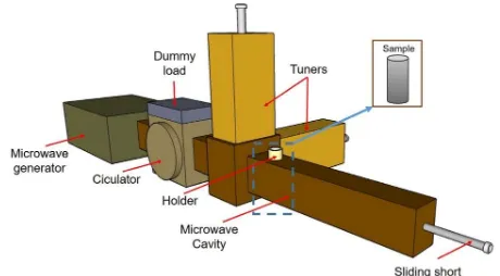
Figure 2-4- Schematic view of the microwave set-up. The sample sits at the center of the waveguide where there is the maximum electric field.
2.5
Scanning Electron Microscopy
17 changing the aperture. Therefore, the system remains stable as long as the lens temperature is held constant.
2.6
Transmission Electron Microscopy
Samples for transmission electron microscopy were prepared by mechanical wedge polishing followed by Ar ion milling using a Fischione Model 1050 ion mill. Two types of transmission electron microscopy (TEM) were used to characterize the microstructure and composition of the samples. The JEOL-2000FX scanning transmission electron microscopy (STEM) with LaB6 electron source was used to take diffraction patterns in parallel beam. For high/atomic resolution and phase/element identification, scanning transmission electron microscopy (STEM) was also performed using a probe-corrected FEI Titan G2 60-300 kV STEM equipped with an X-FEG high brightness source and Super-X™ Energy-dispersive X-ray spectroscopy (EDS) detector operated at 200 kV. The probe convergence semi-angle was 19.6 mrad with a beam current of either 50 or 100 pA for imaging and EDS mapping, respectively. EDS maps were acquired and processed using the Bruker Esprit software.
2.7
X-ray Diffraction
The crystallinity and phases of the samples were characterized by X-ray diffraction (XRD) using a PANalytical Empyrean XRD equipment with Cu-Kα radiation apparatus at 2θ angles of 10-60°. The identification of phases and determination of crystallite sizes were done using the diffraction spectrum.
2.8
Electrical Conductivity and Seebeck Coefficient Measurement
18 and the thermocouples and falsification of the data. The carbon film did not affect the temperature measurement, which was verified with measuring a known reference sample (constantan) from room temperature to 1000 ˚C.
The sample is placed in an enclosed furnace with moderate pressure between lower and upper electrodes. The lower electrode is next to an electrical resistance heater to provide a temperature gradient along the sample. The thermocouple probes used to measure the temperature and voltage of the sample are shown in Figure 2-5-b. To measure the electrical conductivity of the sample, a constant electrical current is sent from the upper electrode through the sample. One wire from each of the thermocouple probes measures the voltage drop across the sample. Data acquisition, analysis and temperature controller are all controlled by software. The electrical conductivity is calculated using the sample’s dimensions and its measured direct current resistance.
The thermocouple probe spacing is measured accurately using a camera sitting in front of the sample. Knowing the sample’s accurate dimensions, the instrument can be calibrated to ensure high degree of accuracy in measuring probe distance which reduces the error in calculating the electrical conductivity.
19 Figure 2-5- ZEM-3 Ulvac setup for measuring electrical conductivity and Seebeck
coefficient.
2.9
Thermal Conductivity Measurement
The laser flash technique was used to correctly determine thermal conductivity of the synthesized samples. This method was developed by Parker et al. in 1961 [86]. The thermal conductivity (κ) of the synthesized samples was calculated according to Equation 2-1:
κ = αρC (2-1)
where α [m2/s] is the thermal diffusivity measured using the laser flash instrument (Netzsch's LFA 457 Micro Flash). α is a quantity that indicates how quickly a material can change its temperature. ρ [kg/m-3] is the mass density of the sample measured using the Archimedes′ principle, and Cp [J/kg K] is the specific heat.
20 thickness to radius ratio of the sample should be less than 0.167. The lower ratio, the more accurate the measurement.
A Pyroceram disk was used as the reference sample in the laser flash apparatus to determine the specific heat of the samples. Either the measured or theoretical specific heat was used to calculate the thermal conductivity of the samples.
Figure 2-6- (a) Netzsch's LFA 457 Micro Flash equipment for thermal diffusivity measurement, (b) schematic cross section of the equipment.
In this experiment, a disk was cut from a 6 mm cylindrical rod and polished to 0.4-0.8 mm thickness. Both sides of the samples were coated with graphite using graphite spray to absorb and match the absorptivity and emissivity. The samples were put in a sample holder made from SiC and placed in the laser flash equipment. The temperature of the sample was monitored using a thermocouple sitting next to the sample. The whole process is carried out in an inert atmosphere.
22
CHAPTER 3:
Fundamentals of Microwave Processing
3.1
Introduction
The term “microwave” is related to alternating signals within the frequency range of 300 MHz to 300 GHz with wavelength of 1 m to 1 mm, respectively. The microwave energy can interact with a material and heat it by volumetric absorption of the electromagnetic energy. In contrast to conventional heating that heats the outside of the material by convection/radiation and inside by conduction, microwave heating heats up the volume of the material [87,88]. Figure 3-1 shows the schematic drawing of the conventional heating and the microwave heating of a bulk sample. The conventional heating is often an energy, time and cost consuming method; however, microwave heating is usually rapid and energy efficient.
Figure 3-1- Schematic drawing of the conventional heating versus microwave heating.
23 was reported. In another study, the interaction of the electric field with highly doped silicon sample resulted in random displacement of the atoms from their lattice position thus creating a temporary lattice strain [90]. It has been also shown that synthesis of nanocrystalline Mg2Si, Bi2Te3 and (Bi0.2Sb0.8)2Te3 is possible using microwave radiation [91,92,93,94] based on rapid heating and prevention of the grain growth. None of these studies produced decrystallized thermoelectric materials. They followed the conventional concept of grain coalescence prevention though the control of the sintering parameters mainly the temperature and processing time.
In microwave sintering the heating mechanism is fundamentally different from other heating methods. Microwave energy interacts with the material at the atomic level [95]. The interaction of the field with the material is dependent on the dielectric properties of the material. It can lead to dipoles rotation and/or the movement of charges. The resultant reaction of the forces (e.g. frictional) lead to dielectric losses which introduce volumetric heating in the material [96,97,98]. The microwave loss mechanisms in non-magnetic materials are mainly categorized into conduction losses and dipolar losses for conductive and dielectric materials, respectively [98]. Microwave cavities can provide means to synthesize and process different types of materials. The materials can be processed in the electric field (E-field), magnetic field (H-field) or a mixture of them.
In a multi-mode microwave field, H-field also interacts with the material. In a single-mode microwave the material heats up quicker due to the higher concentration of the field (E-field or H-field) around the sample. In the E-field, material parameters ε′ and tanδ play the key roles in heating. Apart from these parameters, the microwave frequency also influences the sample heating [90].
3.2
Microwave Processing of Thermoelectric Materials
24 using microwave energy [90,95,101]. The application of microwave processing on decrystallization, microstructure engineering, phase transformation and tuning the thermoelectric properties of materials have not been studied prior to this work. This technique is specially promising as the performance characteristics of the thermoelectric materials can be controlled by degree of decrystallization, the grain size, and composition. With a primary aim of keeping the grain size to a few nanometers, a semiconductor processing method, via microwave processing, is proposed and experimentally implemented.
The decrystallized materials fabricated by microwave processing are different from amorphous materials made by melt-quenching methods (like melt spinning), metallic glasses, or typical glasses. In the XRD patterns of the decrystallized materials, instead of a low angle hump which is the character of the amorphous materials, the intensity of the peaks reduce or the peaks completely diminish and the XRD pattern looks like a flat line with a high background at lower angles than 2θ=15°. Similar observation has been obtained in the microwave processing of highly doped Si [90] and ferrites [95,102]. It is probably due to the extensive distortion of the crystalline grains by ingrained mechanical stress originated from ultra-rapid heating and field quenching [90]. In addition, the background usually increases in XRD patterns. The microwave decrystallized materials are fabricated by heating the material to the melting or sub-melting point and field quenching by switching off the microwave power [90].
3.3
Basic Components of Microwave Setup
All the experiments were done using a custom single-mode TE103 microwave cavity with the maximum input power of 1100 W attached to a magnetron power generator with 2.45 GHz frequency. The E-field is obtained at the center of the cavity while the H-field is near the wall of the cavity. In all experiments the minimum starting power was 60% of the maximum power and a maximum of 80% was reached by the end of the sintering. Powers higher than 80% usually resulted in sparking inside the cavity.
25 the sample. A brief description of each component along with experimental strategies are listed below:
Figure 3-2- Schematic image of microwave setup and the position of the sample.
3.3.1
Magnetron
The microwave radiation is created by a high-power vacuum tube called a “Magnetron”. It is the heart of any kitchen microwave oven today. It produces the required frequency (2.45 MHz) of the microwave energy. The magnetron is classified as a diode made of an anode and a cathode. It does not have the typical grid as in an ordinary electron tube. The external appearance of the magnetrons can be different; however, the internal structures are generally the same. The main components of the magnetron are two magnets, an antenna, the anode (or plate) and the cathode (or filament). The anode is a cylindrical copper block which has even number of holes, known as resonant cavities, which control the output frequency of the magnetron. A narrow slot connects the cavity to the center of the copper block. Each cavity acts like a parallel resonant circuit [103].
26 electrons by the process of thermionic emission. A power supply provides a DC bias accelerating the electrons from the cathode toward the anode.
Two permanent or electro magnets are positioned at the back and front of the block so that a magnetic field is created over the space between the anode and the cathode. The magnetic field is perpendicular to the velocity vector of the electrons.
Between the anode and the cathode, the magnetic field produces a force on the emitted electrons which causes the electrons to move in a circular path and results in a cloud of electrons approaching the anode. The anode is relatively positive and attracts the electrons. This growing spiral propagation of electrons resonates the anode cavities at a specific frequency.
In other word, the magnetic force sweeps the electrons around a circle and pumps the natural frequency of the cavity. The currents throughout the resonating cavities results in the radiation of the microwave at the resonant frequency.
A part of the generated radio frequency (RF) or microwave energy is taken out by a short antenna which is connected to a waveguide which guides the energy to the load. The wall of the waveguide reflects the electromagnetic field and directs the wave into the cavity.
27 Figure 3-3- Magnetron and its cross section [104].
3.3.2 Microwave Cavity
Microwave cavity is a closed hollow metal structure that restricts the electromagnetic field. The cavity acts as a resonator. The microwave bounces back and forth inside the cavity, at certain frequencies, known as cavity’s resonant frequencies, and create standing waves. The cavity allows certain microwave frequencies to pass while prevents other frequencies.
Electric and magnetic energies are stored in the waveguide. There are two main losses inside the cavity including the joule heating of the walls of the waveguide, and the dielectric loss of the atmosphere inside the waveguide. On the cavity walls, due to the boundary conditions which satisfy the resonant of cavity wall, the electric loss tangent, i.e. tanδ, is zero; therefore, the electric field power is zero at cavity walls. The quality factor of a cavity consists of three factors including power loss in the cavity walls, power loss in the filling atmosphere of the cavity, and the power loss through any opening in the body of the waveguide [105].
28
3.3.3 Circulator/Isolator
A circulator is a three-port or four-port component that controls the direction of the wave propagation. An isolator is a type of a circulator which usually has three-ports and is used to mainly protect the magnetron from microwave reflection. An isolator consists of three separate ports including: port 1 connected to the magnetron, port 2 connected to the waveguide, and port 3 which is terminated and connected to a dummy load. A dummy load, such as water, is connected to the circulator and absorbs any reflected power entering port 2. The microwave entering from magnetron reaches port 1 and is transmitted to the waveguide by rotation through port 2. However, the signal which comes from port 2 (reflected power) is transmitted to port 3, which is a dummy load and is absorbed as heat. In a circulator port 3 is not terminated. In a microwave system, an ideal isolator is a compartment that transmits all the entering power from magnetron and absorbs all the power from waveguide. For this purpose, at microwave frequencies, ferrites are used to absorb the reflected power. The interaction of the microwave magnetic field with the ferrites inside the isolator produce a robust rotary magnetic field and let the microwave pass to port 2 but not in reverse. The standard working frequency ranges of isolators are 150 MHz to 40 GHz [106].
3.3.4 E-H Tuner
29
3.3.5 E-H Tuner
Iris (also called window) is a projection from the wall of the waveguide which is used to form the cavity. It is usually placed between the E-H tuner and the waveguide or the applicator. Irises come in different sizes and types. More details is referred to reference [107].
3.3.6 Applicator
An applicator is a part of the waveguide that is used to position the sample inside the cavity. It is designed to heat the material by microwave exposure. It can be in different shapes like batch type, waveguide type, conveyor type, etc. The atmosphere of the applicator can be controlled and can be set to vacuum, air, or an inert gas [108]. In this research, the waveguide type of the applicator was used to heat up the sample and flowing air was blown to reduce the humidity inside the applicator. In a single-mode microwave system, on the applicator, there can be single or multiple hole(s) to put samples inside the applicator, and also to monitor the sample’s temperature.
3.3.7 Sliding Short or Plunger
This component is used at the end of the cavity to make a moveable short circuit inside the waveguide. In fact, the sliding short, also known as plunger, introduces a reference plane in front of the electromagnetic wave and changes the volume of the waveguide [109].
3.3.8 Monitoring systems
3.3.8.1Temperature monitoring system
30
3.3.8.2Microwave Monitoring System
The transmitted and reflected microwave energy should be monitored for proper tuning of the field on the sample. For this reason, an RF detector was used to convert the microwave signals to a detectable DC signal. This signal is inputted to an oscilloscope for monitoring the waveform.
3.4
Basic
Concepts in Microwave Processing
The following are some basic concepts in microwave processing. These include dielectric heating, interaction of materials with microwave, thermal runaway, non-uniform heating, plasma, and electric discharge.
3.4.1
Interaction
of Materials with MicrowaveMaterials can interact with microwave field in different ways. Some materials are transparent to microwave like quartz, BN, MgO, etc.; some materials reflect microwave, like metals; and some absorb microwave like some dielectric materials and semiconductors.
31 Figure 3-4- Schematic representation of the microwave interaction and a diatomic molecule resulting in torque and rotation on the molecule.
3.4.2 Dielectric Heating
Anatom consists of a positively charged nucleus and negatively charged electrons. Any effort to change the path of the electrons or alter the orbitals is accompanied by energy conversion. This energy appears as heat in dielectric heating.
Dielectric heating is a technique in which high energy sources like high frequency alternating electric field or microwave electromagnetic radiation heats a dielectric material. The microwave radiation passes through the sample and heats it via dielectric heating. The microwave radiation is a non-ionizing electromagnetic radiation with a frequency ranging between radio and infrared frequency. The alternating electric field of the microwave can rotate electric dipoles in a material. This rotation can disperse the energy as heat. The material’s temperature increases when the average kinetic energy of the atoms or molecules increases. Therefore, microwave radiation increases the temperature of a material by increasing the rotation and/or torsion of the dipoles. This effect can be applied for any material that contains dipoles [111].
In contrast to metals, electrons in insulators do not flow freely, however, the electronic distortion or reorientation of dipoles can lead to heating. The complex permittivity (known as dielectric constant, ε) is a complex number and conceptually defines as the ability of a dielectric material to absorb and store electrical potential energy. The complex permittivity consists of two components:
32
where ε′ is the real permittivity which characterizes the penetration of microwaves into the material and quantifies the ability of a material to polarize by an external electric field. ε″ is the imaginary part or loss factor, known as the material’s ability to store the energy and it represents the efficiency of the electromagnetic energy which is converted to heat and i is the imaginary constant. The loss tangent, tanδ (also known as loss angle) is defined as the ability of the material to convert absorbed energy to heat. The loss angle is represented as the phase difference between the electric field and the polarization, and it is simply defined as tanδ= ε″/ε′ when there is no electronic or ionic conduction [112,113].
The microwave heating is a process that requires interaction between microwave radiation and dielectric properties or conductivity of a material. This interaction consists of three main parts: (1) space charges caused by electronic conduction, (2) ionic polarization due to far-infrared vibrations, and (3) rotation of dipoles [114].
During microwave heating a material may encounter, one, two or all three of these processes. For the case of materials studied in this research, electronic conduction, σe, ionic conduction σi and the dielectric loss due to the complex permittivity, ε=ε′-iε″ each can be significant depending on the sample temperature during the microwave radiation. If an electric filed, Eext, applied to the material is:
= (3-2)
The current density, j, according to the Maxwell equations is:
= + + ( − ) = + tan (3-3)
Where
tan =
( + )+ (3-4)
33 microwave heating is tanδ, known as loss tangent. The average stored electric energy per unit volume is defined by:
=1 2
(3-5)
The average power which is converted into heat per unit volume is:
=1
2 tan
(3-6) Therefore, the loss tangent shows the ability of the material to convert absorbed microwave power into heat depending on the frequency, the loss factor, the permittivity and the electric filed intensity. A material with high tanδ is known as lossy material while a material with low tanδ is known as low-loss material. A lossy material heats up more efficiently than a low-loss material.
In the microwave frequency ranges, electronic conductivity does not remarkably change with the frequency. However, temperature can vary the conductivity depending on the transport mechanisms in the material [108].
In semiconductors and metal-like materials, electronic conduction plays an important role on heating. Materials with medium conductivity heat more efficiently than isolators or highly conductive materials. Although the microwave penetration in low loss insulators is high, they cannot heat up. A rapid improvement in conductivity leads to a rapid change in loss which will result in uneven heating or thermal runaway in the material being radiated by microwave field. In highly conductive materials, due to the skin effect, the field reduces toward the inside of the sample.
34 Dielectric heating (known as dipolar heating) is mainly due to two main effects. If the charged particles can freely travel through the material, a current will be induced which travels in phase with field. It is known as conduction. If the charged particles are tightly bonded in a material, the electric field results to move them until equalize the opposing forces. This is called dipolar polarization. Both conduction and dipolar polarization cause heating in the material.
The microwave absorption in a material is temperature and frequency dependent. The concept of these dependencies are briefly discussed below, however, the details of these analysis are beyond the scope of this research.
Both real (ε′) and complex (ε″) dielectric constants are frequency (Figure 3-5) and temperature dependent. The microwave absorption happens in the range of frequencies that dielectric loss (ε) is not zero. According to Debye equations [115,116], the temperature dependency of ε′ and ε″ in liquids is calculated by:
= + ( − )
(1 + )
(3-7)
=( − )
(1 + )
(3-8)
where and are dielectric constants at high frequency (infrared) and static field, respectively, and τ is the relaxation time derived from Stoke’s theorem:
= 4 (3-9)
35 Figure 3-5: Frequency dependency of ε′ and ε″ [118]. The microwave frequencies are highlighted and the frequency range of the microwave used in this study (2.54 GHz) is shown by a red dashed line.
Figure 3-6: ε′ and ε″ calculated as a function of ωτ based of Debye expression [115,116].
36 constant gradually decreases. At Tm, the structure of the material changes, hence, the dielectric constant alters. At melting point, the dielectric constant can increase or decrease. This temperature can also be the phase transformation temperature in which the structure of the material changes. Above Tm, the average alignment of dipoles decreases, therefore, the dielectric constant reduces [119].
Figure 3-7: Schematic diagram of the temperature dependency of dielectric constant [119].
The dipoles in solids are not free to rotate as well as in liquids. They are restricted by other dipoles and separated by potential barriers. The theoretical model for solids is calculated similar to the liquids with minor revisions. Assume that there are there are two potential wells which are separated by a potential barrier. For a possible orientation of dipoles, according to the statistical mechanics, the relaxation time is related to the potential barrier by:
= (3-10)
Where A is a temperature dependent constant, and W is the energy of the potential barrier. Dipolar solids generally show small dielectric losses due to their large W [120].
In addition to the dielectric loss, several materials exhibit conduction loss under microwave radiation. In conduction loss, the complex dielectric constant is defined by:
∗ = + −
1 + −
(3-11) Temperature Tm
37 The dielectric losses of the solids comes from the conduction term and are affected by temperature. The loss factor of the ceramics generally increases with temperature; the rate of increment depends on the type of ceramic and the frequency (Figure 3-8) [98]. In microwave heating of solids, the increase in dielectric properties with temperature is important because it can result thermal runaway or uncontrolled rise in temperature [121]. According to Figure 3-8, the microwave heating of Al2O3 is negligible at room temperature, while by increasing the temperature the loss factor enhances and microwave heating is more effective.
Figure 3-8- Temperature dependence of Tan δ for Glass, Al2O3, SiO2 and Al2O3 [98].
It should be considered that although other mechanisms like atomic and ionic polarizations exist, they do not contribute to microwave heating.
3.4.3 Non-uniform Heating
38 sample should be uniform. Besides these mentioned issues, the sample geometry can also contribute in non-uniform heating. For example, narrow sections tend to heat up rapidly due their smaller volume; therefore, the sample being radiated by microwave should be uniform in shape as much as possible without any sharp edges.
3.4.4 Thermal Runaway
When a sample is exposed to microwave, one or multiple parts on the sample can undergo thermal runaway and locally heat up rapidly; these areas are called hotspots and they are caused by inhomogeneous heating. In comparison to the other parts of the sample a localized spot can reach very high temperature, i.e. melting point of the sample, while the average macroscopic temperature still remains low. Hotspots may be created by uneven distribution of the electromagnetic field in the sample and/or dielectric property variation in a material which results in non-uniform heating [122,123]. To avoid hotspots during microwave sintering or decrystallization, the heating rate should be controlled. Modulation-controlled microwave processing can help reduce the chance of hotspot formation. Thermal runaway in microwave process is almost inevitable due to the nature of absorption which usually increases with temperature; therefore, special attention must be taken to control the temperature during the microwave processing of materials.
3.4.5 Plasma
39 sample and the plasma, and a higher degree of ionization occurs. More detailed information is referred to [124]. Microwave plasma has several applications like surface modification, sintering, film deposition, etc. The microwave plasma is produced in a closed chamber at low or high gas pressure, or in an open chamber under gas flow.
The microwave heating of thermoelectric materials can happen with or without plasma and each has different characteristics. In our experiments for decrystallization of the thermoelectric materials, we generally avoided plasma formation to acquire uniform volumetric heating. Thermoelectric materials are usually highly doped to increase their electrical conductivity. In some materials such as highly doped silicon germanium, at high temperature, once plasma forms, dopants start to diffuse more to the surface of the sample due to their higher solubility at higher temperature. This results in a conductive cladding around the sample. As a result, the conductive cladding reflects the microwave and shields the center of the sample from microwave penetration.
3.4.6 Electric Discharge
The electric discharge, spark, electric arc, or corona discharge is an electrical breakdown of the gas or the plasma. The breakdown voltage depends on the type of surrounding gas and the pressure. Both the high temperature and high power increase the chance of sparking. In microwave processing, to obtain a uniform sample, sparking must be prevented.
3.5
Conclusions
40
CHAPTER 4:
Microwave Processing of Thermoelectric
Materials
4.1
Introduction
If the density of point defects in a crystalline material becomes very high, the material undergoes a phase transition to an amorphous state where neither long range nor short range order of the atoms can be found. Amorphous phases can possess fundamentally different electrical and thermal properties than crystalline or nano-crystalline forms of the same thermoelectric (TE) materials [79].
The interfaces in amorphous materials introduce sites for scattering of charge carriers and phonons, which is an important phenomenon in energy materials, such as TEs. In general, in nanostructured materials the interfaces result in resistance to electrical and thermal energy transport. They not only cause electron and phonon scattering, resulting in electrical and thermal resistance, but also break any long-range periodicity of the material comprising the interfaces. Moreover, the interfacial region in a nanostructured material can itself be amorphous. In fully amorphous materials the interfaces do not exist and both short and long range periodicities are lost. For example, instead of bands and gaps, band tails and localized states are distinguishable in their quasi-continuous energy spectrum. Localization of electronic states can happen at certain sites or in certain regions of the amorphous material. As more band states are localized, the disorder raises and it is more likely that the localized states will be close to the band edges [78].
41 zT, one has to increase the power factor simultaneously while reducing the thermal conductivity.
zT in amorphous (and fine grained) TEs was conceptually studied by Nolas and Goldsmid in 2002 [80]. Under several simplifying assumptions, they described the conditions under which an amorphous material should have a large figure of merit. Although fine grained TE materials have been investigated vastly since then, there has only been limited reports on the development of amorphous based TE structures [81].
What is needed is a new way of creating a state of amorphous and amorphous-crystalline in materials. Further, (1) a method that is scalable to produce high efficiency bulk TE structures as well as thin and thick films is needed, (2) a method that enables control over the volume of the amorphous domains in a crystalline TE material is needed, and (3) a methods that enables control over the density and porosity of the TE material is needed.
Most experimental studies on electronic, optical, or thermal properties of amorphous materials in the past have been concentrated on their thin film structures [79,130]. For example, the discovery of how to dope amorphous silicon thin films, thereby producing p-n junctions, enabled the development of amorphous diodes, now widely used in solar cells. In addition, the development of field effect transistors from amorphous silicon opened up its use in flat screen displays. Current research on amorphous thin film silicon includes memory devices, field-effect transistors and image sensors [131].
42 Microwave energy is a rather quick and convenient method which has been widely used to synthesize and sinter different class of materials including metals/alloys [137,138,139,140] and ceramics/semiconductors [141,142,143,144]. There are also some studies on the effect of microwave energy on powder processing of thermoelectric materials [93,99,145,146,147,148,149,150,151,152,153]. However, it has not demonstrated improvement of the thermoelectric properties through in-situ amorphization/decrystallization of the bulk thermoelectric material in a microwave oven or cavity.
In this chapter, we propose and develop microwave processing as a promising method to produce bulk material structures based on amorphous/decrystallized and/or mixture of amorphous/decrystallized and polycrystalline phases, namely amorphous-crystalline composites. This results in significant enhancement of the TE power factor, which along with the reduction of the thermal conductivity, can be compared with the single crystalline, polycrystalline, or nano-crystalline form of the same constituent materials. This method provides an extraordinary route to create a state of amorphous/decrystallized and amorphous-crystalline materials in a quick and convenient way. The simple procedure and quick processing time of the method allows investigating a large number of TE materials with various dimensions. The present method proposes a scalable technique to produce high efficiency bulk TE structures as well as thin and thick films.
In this chapter, the capability of microwave processing on amorphization/decrystallization and phase transformation of different materials is studied and the materials are characterized. In the following chapters, the application of microwave processing on sintering, decrystallization and thermoelectric properties of different thermoelectric materials will be discussed.

![Figure 1-3- (a) High resolution transmission electron microscopy image of a hot pressed Bi0.5Sb1.5Te3 and (b) comparison of the zT of nano-grained and micro-grained (Bi,Sb)2Te3alloy [31]](https://thumb-us.123doks.com/thumbv2/123dok_us/1509615.1184880/30.612.100.530.305.495/figure-resolution-transmission-electron-microscopy-pressed-comparison-grained.webp)


![Figure 3-5: Frequency dependency of ε′ and ε″ [118]. The microwave frequencies are highlighted and the frequency range of the microwave used in this study (2.54 GHz) is shown by a red dashed line](https://thumb-us.123doks.com/thumbv2/123dok_us/1509615.1184880/58.612.142.487.75.281/figure-frequency-dependency-microwave-frequencies-highlighted-frequency-microwave.webp)


