ABSTRACT
MCGREGOR, JR., DAVID ROSS. Growth Optimization and Characterization of Reactively Sputtered Zirconium Nitride Thin Films for III-V Buffer Layer Applications (Under the direction of Jerome J. Cuomo)
Zirconium nitride (ZrN) thin films were deposited by reactive dc magnetron sputtering to assess the effects of processing conditions upon film properties. Processing conditions and parameters were optimized to generate films of completely oriented (111) ZrN on silicon to be used as buffer layers for the growth of gallium nitride A single and double Langmuir probe were used to determine trends in electron temperature, ion density, ionization fraction, and floating potential during reactive sputtering of zirconium in argon and nitrogen. Reactive gas concentration, deposition pressure, deposition temperature, cathode current, film thickness and substrate orientation were investigated as variable processing conditions. Four-point probe, scanning electron microscopy (SEM), transmission electron microscopy (TEM), Raman spectroscopy, and x-ray diffraction (XRD) were used to characterize thin films produced.
for Mer
BIOGRAPHY
ACKNOWLEDGEMENTS
I would first like to thank Dr. Jerome J. Cuomo for his continued support, guidance, and energy throughout the course of this research. The experience and knowledge I have gained at the Center for Advanced Manufacturing Processes and Materials (CAMP-M) has taught me to question all, hunt the truth, and thirst for more.
I thank Dr. Mohamad Bourham for his countless hours of support and plasma science instruction. I thank Dr. D. Maher for his support and guidance through an undergraduate and graduate career. I would especially like to thank Mark Williams, Dr. Jung Won Cho, and Dr. Minseo Park for there invaluable time, teachings, and insights in plasma processing and characterization. I wish to express my sincere gratitude to my better half, Merri, for her overwhelming support, kindness and a strong willingness to put up with me. I would also like to thank my parents, Dave and Ruth, for there unwavering encouragement and support.
Table of contents
Page
List of Tables ... viii
List of Figures ... ix
1.0 INTRODUCTION... 1
1.1 IV-B Transition Metal Nitrides ... 2
1.2 The Sputtering Phenomena... 3
1.2.1 Plasma Generation... 3
1.2.2 Ion Bombardment... 8
1.2.3 Atomic Transport... 11
1.2.4 Nucleation and Growth... 12
1.3 Practical Aspects of Sputtering... 15
1.3.1 Epitaxial Growth... 15
1.3.2 Reactive Sputtering... 16
1.3.3 Radio-frequency Sputtering... 17
1.3.4 Sputter Yield... 18
1.4 References ... 19
2.0 EXPERIMENTAL STRUCTURE... 23
2.1 Dual Magnetron... 23
2.2 Self Sputter Magnetron... 25
2.3 Magnetrons ... 29
2.3.1 Balanced versus Unbalanced Magnetron Sputtering... 31
2.3.2 DC Magnetron Sputtering... 32
2.3.3 Pulsed DC Sputtering... 33
2.4 Plasma Characterization ... 34
2.4.1 Pressure Effects on I-V Characteristics... 34
2.4.2.1 Single Probe... 37
2.4.2.2 Double Langmuir Probe ... 41
2.5 Thin Film Characterization... 44
2.5.1 Raman Spectroscopy... 45
2.6 Gallium Nitride... 47
2.6.1 Lattice and Thermal Expansion Mismatch... 48
2.7 References ... 50
3.0 ZIRCONIUM NITRIDE... 54
3.1 Properties of IV-B Transition Metal Nitrides... 54
3.2 Properties of Higher Zirconium Nitride ... 55
3.3 Deposition of Zirconium Nitride ... 56
3.4 GaN growth on ZrN... 57
3.5 References ... 59
4.0 OPTIMIZATION OF REACTIVE MAGNETRON SPUTTERING OF ZIRCONIUM NITRIDE ... 61
4.1 DC Reactive Magnetron Sputtering of Zirconium Nitride and Gallium Nitride Thin Films... 61
4.2 Processing Condition Effects upon the Resistivity of Zirconium Nitride Thin Films ... 62
4.2.1 Effect of Reactive Gas Concentration upon the Resistivity of ZrN Thin Films ... 62
4.2.2 Effect of Deposition Pressure upon the Resistivity of ZrN Thin Films... 63
4.2.3 Effect of Cathode Current upon the Resistivity of ZrN Thin Films... 64
4.2.4 Effect of Deposition Temperature upon the Resistivity of ZrN Thin Films... 65
4.3 Processing Condition Effects Upon the Crystallinity of Zirconium Nitride Thin Films ... 66
4.3.1 Effect of Deposition Pressure upon the Crystallinity of ZrN Thin Films... 66
4.3.4 Effect of Substrate Orientation upon the Crystallinity of ZrN Thin Films... 71
4.3.5 Effect of Film Thickness upon the Crystallinity of ZrN Thin Films... 72
4.4 Microscopic and Spectroscopic Investigation of ZrN Thin Films ... 74
4.5 Summary and Conclusions ... 79
4.6 Future work... 80
LIST OF TABLES
Page
Table 2.1. Electron temperature and ion density at 0.5 ampere...41
Table 2.2. Electron temperature and ion density at 1.0 ampere...42
Table 2.3. Double Probe Characterization Results...45
Table 2.4. Gallium nitride material properties...49
Table 2.5. Lattice mismatch between substrate materials/buffer layers to gallium nitride...50
Table 2.6. Thermal Expansion Coefficients of Silicon, Sapphire (0001) and ZrN...51
Table 3.1. Properties of ZrN...56
LIST OF FIGURES
Page
Figure 1.1. Schematic of a typical sputter deposition system... 5
Figure 1.2. Paschen plot... 6
Figure 1.3. Schematic of regions of a diode plasma sputtering system... 7
Figure 1.4. Gas discharge classification as a function of discharge current ... 8
Figure 1.5. Schematic of the three sputtering regimes... 9
Figure 1.6. Collisional processes within the sputter process ... 10
Figure 1.7. Ion - Target impact in the sputter process ... 10
Figure 1.8. Schematic of the potential distribution in a typical diode plasma... 11
Figure 1.9. Initial growth stages in the sputter deposition process... 13
Figure 1.10. Schematic representation of the influence of substrate temperature and argon working pressure on the structure of sputtered thin films... 14
Figure 1.11. Reactive sputtering hysteresis ... 17
Figure 1.12. Sputter yield... 18
Figure 2.1. Schematic of dual magnetron sputter deposition system ... 23
Figure 2.2. CAMP-M dual magnetron sputter deposition system ... 25
Figure 2.3. Schematic self sputter magnetron deposition system... 26
Figure 2.4. The center for advanced manufacturing processes and materials self sputter magnetron.... 28
Figure 2.5. Cross-section of a planar magnetron ... 29
Figure 2.6. Electron in the presence of magnetic and electric fields ... 30
Figure 2.7. Cross-section of balance magnetron showing magnetic field lines and electron orbit. ... 31
Figure 2.8. Unbalanced magnetron... 32
Figure 2.10. Dual magnetron magnetic field arrangement ... 34
Figure 2.11. Effect of applied voltage as a function of current for the Advanced Energy DC magnetron power supply operating in constant current mode sputtering... 35
Figure 2.12. Circuitry schematics of CAMP-M Langmuir probe... 36
Figure 2.13. Typical single Langmuir probe I-V curve ... 38
Figure 2.14. Single probe measurement of dc zirconium sputtering at 0.5 Amps, 5 mTorr at the substrate center ... 40
Figure 2.15. Typical double Langmuir probe characteristics ... 42
Figure 2.16. Nitrogen concentration effects upon the current-voltage characteristic of zirconium sputtering measured with double Langmuir probe ... 42
Figure 2.17. Schematic of four point probe set up... 44
Figure 2.18. Typical Raman spectroscopy plot ... 46
Figure 3.1. Proposed structure for Zr3N4... 56
Figure 3.2. NaCl (111) orientation and it’s relation to the hexagonal structure ... 57
Figure 4.1. Resistivity of zirconium nitride as a function of reactive gas concentration at constant current ... 62
Figure 4.2. Resistivity as a function of sputtering pressure at 500C, 4% nitrogen concentration, and 0.5 Amp. cathode current on Si(111)... 63
Figure 4.3. Resistivity as a function of cathode current on silicon (111) and silicon (100) substrates ... 64
Figure 4.4. Effect of ZrN deposition temperature on resistivity for films deposited at 0.5 ampere cathode current, 5mTorr, and 4% nitrogen concentration... 65
Figure 4.5. Effect of pressure upon crystallinity of ZrN on (111) silicon substrates at 500° C, 0.5 ampere cathode current and 4% nitrogen... 67
Figure 4.6. Effect of deposition pressure upon crystallinity of zirconium nitride deposited upon silicon (100) at 500°C, 4% nitrogen and 0.5 ampere cathode current ... 68
Figure 4.8. Effect of cathode current on the crystallinity of ZrN reactively sputter
deposited on silicon (111) ... 70
Figure 4.9. Effects of temperature upon the crystallinity of ZrN thin films deposited on (111) silicon substrates... 71
Figure 4.10. Substrate orientation upon the cyrstallinity of ZrN thin films deposited at 500°C, 4% N2, 5 mTorr... 72
Figure 4.11. Effect of thickness upon the crystallinity of ZrN deposited on (111) silicon samples at 0.5 amp, 10 mTorr, and 4% nitrogen concentration... 73
Figure 4.12.. Proposed critical thickness model for the titanium nitride system... 74
Figure 4.13. Cross-sectional SEM micrograph of ZrN on silicon ... 75
Figure 4.14. Transmission Electron Micrographs of GaN thin films grown on ZrN ... 76
Figure 4.15. Raman spectroscopy analysis of ZrN as a function of deposition pressure 77 Figure 4.16. Raman Spectrum of Zr3N4 thin films deposited on (100) silicon at 500°C, and 0.5 amp, and 100% nitrogen, as a function of temperature3... 78
1.0 INTRODUCTION
Over the course of the last several decades, the world has seen an exponential increase in technological advancement. Particularly, in the area of solid state physics and thin film processing to either improve or alter certain material properties, to enhance existing circuitry or to generate entirely new materials. As the need for improved film control with smaller feature sizes becomes necessary, manufacturing techniques must likewise be improved to accommodate. Techniques such as molecular beam epitaxy (MBE), ion implantation, physical vapor deposition (PVD), chemical vapor deposition (CVD), electron beam evaporation, plasma enhanced chemical vapor deposition (PECVD) and high vapor phase epitaxy (HVPE) have been developed to provide a means of manufacturing high quality materials and coatings. As these techniques have evolved in the global market place, academia has continued to use them to investigate a host of materials and processing capabilities. J. Georg Benorz and K. Alexander Müller, of IBM Research, were presented the Nobel Prize in 1987 for the study of a thin films problem1.
To carefully control the properties of thin films, processing steps must also be carefully controlled. Investigations and examinations must be undertaken in order to understand the effects processing conditions have upon the outcome of any experiment or process. Designed experiments and statistical processes are increasingly utilized in industry for quickly identifying variables that affect a response of interest.
1.1 IV-B Transition Metal Nitrides
Super-hard coatings, such as the IV-B transition metal nitrides, carbon nitrides and diamond-like carbons (DLC), have been used primarily to protect components in high friction environments from wear. Their high strength and low coefficient of friction permit the use of these materials in industries ranging from the food processing industry to decorative coatings and have recently been examined by the microelectronics industry. The IV-B transition metal nitrides, specifically, have been investigated for a number of years for a wide variety of applications. Produced as a thin film, they demonstrate high hardness2,3, chemical stability4, corrosion resistance5, high melting point6, low resistivity7 and low coefficient of friction8. Recently, these IV-B transition metal nitrides have been investigated as diffusion barriers9,10,11,12,13 in metallization schemes, superlattice constituents14,15,1, field emitters16, electrical contacts to III-V semi-conductors17, Josephson junctions18, and cryogenic thermometers19.
Zirconium nitride (ZrN) and titanium nitride (TiN) coatings provide the look of gold with the strength of steel. The coating of watch bezels, drill bits, outdoor lighting and window glass are several of the more popular uses of these nitrides. With such a broad range of applications, it becomes increasingly important to clarify and quantify the effects processing parameters have on the growth and properties of ZrN and identify new uses of the resulting materials.
1.2 The Sputtering Phenomena
Sputtering is a physical vapor deposition (PVD) process where material is physically removed from a target by energetic ion bombardment. The term sputtering comes from the Dutch “sputteren” meaning “to spit out in small particles and with a characteristic explosive sound”23. Sputtering was first observed by Groves in 1852 with Plücker first to suggest, in 1858, that this discovery be used as a tool to produce metallic films24. Groves initially called the phenomena “cathodic disintegration”, and it was renamed “spluttering” by Sir John Thompson in 192125. In 1923 Thompson dropped the “l” and the term “sputtering” has lasted to this day.
Sputtering is referred to as a physical process as it is simply a momentum exchange between particles with no chemical reactions occurring. Early plasma processing found removal of material from the cathode to be an inconvenience, as the destruction of the cathode would result. Others, however, including Edison, Wright, Faraday, and Crookes, saw the potential of such a device and began investigating the technique26. Today, sputtering is a powerful tool used for the deposition of thin films, in chemical analysis, etching and cleaning. Sputtering is commonly utilized for thin film deposition, as the extremes for melting or chemically reacting high melting point materials are not required, as with evaporation or an electrochemical process.
There are four main processes that occur during sputtering: plasma generation, ion bombardment, atomic transport, and nucleation and growth at the substrate. These will be individually discussed, as each of the four have effects upon the growing film.
1.2.1 Plasma Generation
Pressure is related to number the density of particles per cubic meter by the perfect gas law29
nkT
P= [1.1]
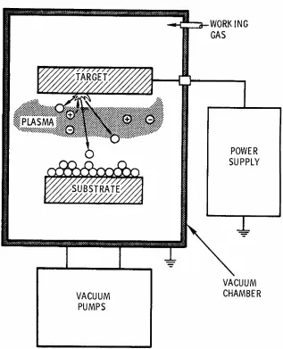
Figure 1.1. Schematic of a typical sputter deposition system30.
In its basic form, a planar diode sputtering device consists of two opposing, flat electrodes in an evacuated chamber. A variety of power supplies are available for plasma generation, ranging from dc to ac with frequencies into the mega-hertz. In dc sputtering a potential difference of several hundred volts is generated between the two plates creating an intense electric field between them. The electric field is given by
d V
E= [1.2]
A free electron placed near the cathode, by a UV photon or cosmic ray, will be accelerated in the direction of the field32. As the electron is propelled toward the anode it will encounter gas atoms contained between the electrodes. This is generally a high purity noble gas at a reduced pressure. The impact of a high-energy electron with a gas atom will ionize the atom by the ejection a weekly bound outer shell electron. The ejected electron is subjected to the same field and will also be accelerated toward the anode. This avalanche effect of electrons is responsible for the breakdown and sustained ionization of the gas.
The voltage at which this occurs is known as the breakdown voltage (Vb). The minimum breakdown voltage can found from plotting breakdown voltage versus pressure times electrode spacing, as seen in figure 1.2, described by a Paschen law24
b pd pd a Vb
+ =
log [1.3]
where Vb is known as the breakdown voltage (typically on the order of 1-6kV10), p is the gas pressure, d is the separation distance of the electrodes, and a and b are constants11.
Figure 1.2. Paschen plot33.
There are four important processes that occur within the plasma in order to sustain a “quasi-neutral gas of charged particles”23: Ionization, Excitation, Relaxation and Recombination. The most prevalent of which is electron impact ionization as seen here:
As can be seen in equation 1.4, with each electron collision two electrons and an ion will be produced. As the process continues, the generation of two electrons from a single electron impact leads to an avalanche effect (Townson discharge) and will only sustain a plasma if every collision emits more than one electron on average. Excitation is a process of electron promotion to a higher energy state, which is short lived due to recombination and photon generation.
e- + Ar → Ar* + e- [1.5]
Relaxation occurs as the electron relaxes from an excited state to its ground state. As the electron relaxes a photon is given off with an energy corresponding to an energy difference that is elementally specific. It is this process that is a function of all plasmas and responsible for the term “glow discharges”33. Recombination occurs as ions and electrons within the plasma recombine to form neutral molecules.
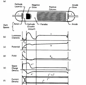
This avalanche effect provides a self sustaining nature, and charge equilibrium will be found with the procurement of characteristic dc sheaths as seen in figure 1.3.
The cathode sheath is a region of large voltage drop with low electron density. It is across the cathode dark space where a majority of the applied target voltage is dropped23. The cathode sheath contains few electrons, as they are repelled as soon as they enter the sheath. Ions, however, are drawn out of the plasma edge and are accelerated across the sheath as seen in Fig 1.6. There are a variety of ion-cathode interactions, which will be covered in the next section.
There are four distinct glow regimes defined by the discharge current as seen in Figure 1.4. Below a discharge current of 10-9 A, the secondary electron emission is so low that there is not enough ionization to produce a self-sustained discharge. As the discharge current increases, the glow will eventually engulf the cathode in the abnormal glow regime. As discharge current increases further the discharge will move into the arc regime.
Figure 1.4. Gas discharge classification as a function of discharge current33.
1.2.2 Ion Bombardment
Powell and Rossnagel state there are four different results obtained depending upon the kinetic energy (E) of the bombarding ion25. The modern theory of sputtering, developed by Peter Sigmund34, states that at low kinetic energies, or the “subthreshold region”, where E = 0-50 electron volts (eV), the ion does not have enough energy to dislodge target atoms. At moderate energies or the “knock-on sputtering regime”, where E = 50-1000 eV, ions impact and dislodge “knock-on” atoms into the target, these knock on atoms impact and dislodges other target atoms. This results in a collision cascade that ejects atoms, ions, electrons and neutrals from the first 10 to 50Å of surface of a target35. Several researchers have shown that the ions must exceed four times the binding energy of the target atoms to induce sputtering25, 35. It is within this regime that most practical PVD systems are operated. At high energy, where E = 1-50 keV, impacting ions penetrate into the lattice and are implanted. At very high energies, E >50 keV, ions penetrate deep into the lattice and are implanted within the bulk. While these latter two processes are used for material doping and implantation, it is virtually irrelevant to sputtering. The three regimes of sputtering by elastic collisions are seen here. For metallic targets, the elastic collision processes are the most important34.
a. single-knock-on b. linear cascade c. spike
Figure 1.5. Schematic of the three sputtering regimes34.
Figure 1.6. Collisional processes within the sputter process30.
Figure 1.7. Ion - Target impact in the sputter process30.
Momentum transferred from ion impact to target atoms will drive the surface target atoms into the target. Sputtering, therefore, requires a sequence of collisions. A collision cascade arises from multiple interactions of bombarding gas atoms with target atoms, as the ions impart their energy over a distance within the surface of the target.
In a steel vacuum chamber, fast moving electrons within the plasma are drawn out toward the chamber walls and other grounded surfaces. The more mobile electrons will be removed from the plasma at a rate greater than that of the heavier ions, leaving the plasma more positive than its surroundings. If an electrically isolated medium is inserted into a plasma, the same situation arises; however, a negative charge will build and upon reaching equilibrium leaves the medium at a negative potential known as the floating potential. This is given as the negative of the plasma potential
+ − = Φ e i i e e f T T m m e
kT 2 1
ln 5
.
0 π [1.6]
where k is the Boltzmans constant, Te and Ti are the electron temperature and ion temperature respectively, me and mi are electron and ion mass respectively and can be seen graphically in figure 1.8.
Figure 1.8. Schematic of the potential distribution in a typical diode plasma30.
These electrically isolated surfaces are at a negative potential relative to the plasma. Electrons will initially be repelled from these surfaces until equilibrium is reached such that the plasma potential (Vp) is several volts more positive than it’s surroundings
1.2.3 Atomic Transport
distance between cathode and anode (d) have a statistical probability of collision with gas atoms, known as the collision cross-section. The mean distance a gas molecule can travel before collision with another gas molecule is known as the “mean free path” (l) and is given by:
n d
l 2
2 1 π
= [1.7]
where n is the molecular concentration (molecules/m3) and d is the diameter of the molecule36. At a pressure of 10-2 Torr, the mean free path is roughly 5 mm37.
At low pressures, or the ballistic transport regime25, sputtered particles will have few gas phase collision and arrive at the substrate with their initial kinetic energy. These energetic bombarding species can have beneficial or deleterious effects upon the substrate and the growing film.
At higher pressures, or shorter mean free paths, sputtered atoms collide with gas atoms and transfer energy through elastic collisions, thereby thermalizing with the gas, the outcome of which is a decrease in sputtered atom energy as a function of increasing pressure or increasing distance between cathode and anode33. This type of transport is referred to as diffusive transport.
1.2.4 Nucleation and Growth
The coalescence growth stage occurs when these islands grow large enough to touch and continues until the film reaches continuity38. The islands start to coalesce to reduce the overall surface area of the growing film. This tendency to form larger islands is known as agglomeration24. When the islands grow together, the film is said to go from a discontinuous islands type to a porous network type24. This type of growth will continue until all islands have grown together and will a continuous film.
Depending upon the conditions for deposition, there are three initial nucleation and growth stages. Films grown by coalescence of islands are known as Volmer-Weber type24. Volmer-Weber occurs when sputtered atoms are bound more tightly to each other than the substrate, such as in the growth of metal films on insulators39. Films that grow layer by layer are known as Frank-van der Merwe type. Frank-van der Merwe growth occurs when lattice mismatch is small and the binding energy of sputtered atoms is equal to or less than the binding energy of sputtered atoms to the substrate39. Those that grow by a mixture of the two are called Stranski-Krastanov type24. A graphical summary of the initial stages of growth can be seen in figure 1.9.
Figure 1.9. Initial growth stages in the sputter deposition process1.
In most cases, thin films are formed by the coalescence of islands. When these islands grow together, various defects and grain boundaries are formed. Grains that coalesce with randomly oriented directions will produce a polycrystalline film.
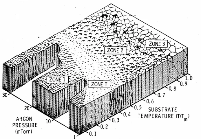
function of deposition temperature, melting temperature (T/Tm) and deposition pressure30. The model consists of four zones as seen in figure 1.10.
Figure 1.10. Schematic representation of the influence of substrate temperature and argon working pressure on the structure of sputtered thin films30.
Zone 1 films occur when adatom mobility is not enough to overcome the effects of shadowing and results in a fibrous film separated by voids. As T/Tm increases, so too does the crystallite size. Zone T is known as the transition region where the adatom mobility is sufficient to overcome the shadowing effects and results in a smoother surface than in Zone 1 films. Zone 2 is a region dominated by surface diffusion growth with increasing grain size separated by intercrystalline boundaries30. Zone 3 is a region characterized by elevated growth temperatures. At these temperatures adatom mobility results in bulk diffusion and equiaxed grains. At sufficiently high substrate temperatures and sufficiently lattice matched substrates, epitaxial growth can be achieved30.
1.3 Practical Aspects of Sputtering
1.3.1 Epitaxial Growth
The term epitaxy comes from the Greek meaning “to arrange” (taxia) “upon” (epi)39. Epitaxial growth is essentially the reproduction of the structure of a substrate in a thin film. Epitaxy can be achieved in two ways: either through the growth of a material upon a substrate of that identical material (homoepitaxy), or the growth of a material upon a substrate of different material (heteroepitaxy). The first successful attempt of which was performed by Frankenheim, in 1836, with parallel oriented growth of sodium nitrate on calcite, with a systematic study later performed by Barker41. The discovery of the diffraction of X-rays in 1912, led to the development of x-ray diffraction devices and transmission electron microscopy (TEM) which allowed for the quantitative examination of epitaxial produced material.
One of the most important conditions for growth of epitaxial films is the substrate temperature. There exists a critical temperature, known as the epitaxial temperature (Te), at which epitaxy will occur41. Epitaxial deposition temperatures must be relatively high to allow for large scale atomic movement and arrangement upon the substrate. This requires that the thermal expansion coefficients of the material system be well matched. At low temperatures, atoms generally condense where they arrive as thermal energy is quickly withdrawn. However, with elevated substrate temperature, the addition of thermal energy to the substrate allows for increased adatom movement and the time necessary for atomic ordering. Epitaxial deposition of metallic films on semiconductors is of interest for metal based transistors and three-dimensional integrated circuitry42.
energy state and will strain the first few mono-layers in order to accommodate the films lattice constant. This effect is known as pseudomorphism, or pseudomorphic growth31.
The use of single crystal silicon substrates is the basis of today’s chip technology. As the push for high power, high frequency circuitry has stretched the limits of silicon processing technology; other materials capable of meeting these needs are being developed. Single crystal wide bandgap semiconductors, such as gallium nitride (GaN), are currently being developed to meet the needs of tomorrows chip processing technology. GaN, however, suffers from a lack of suitably thermal and lattice matched substrates. Sapphire and silicon carbide wafers are today the most widely used substrates for these applications. The expense of these wafers has fueled research of buffer layers grown on Si that can accommodate the strain produced during thin film growth and result in closely matched surfaces. Nitronex43 is one such company using buffer layers on silicon to produce GaN based high power, high frequency circuitry.
1.3.2 Reactive Sputtering
DC reactive sputtering has been used to generate a host of high quality nitrides: NbN(44), TiN(45,46), AlN(47,48); and oxides: PtO(41), TiO2(38). Reactive sputtering is an advantageous method for formation of complex products from the reaction of elemental metal targets and reactive gases. This eliminates the need for construction of expensive compound targets or the use of highly volatile gases.
metal, a decrease in deposition rate will occur. This is referred to as the non-metallic or poisoned mode of sputtering as the target is said to be “poisoned”49. The effect is generally described in terms of a hysteresis examining the deposition rate versus reactive gas concentration as seen in figure 1.11. Once poisoning of the target occurs, and the partial pressure of reactive gas is reduced, the deposition rate will not increase again until the reacted material on the surface of the cathode has been removed.
0 20 40 60 80 100 120
0 2 4 6 8 10 12 14
Reactive Gas Concentration (%)
D ep os iti on R at e ( nm /m in. ) Increasing Reactive Gas Concentration Decreasing Reactive Gas Concentration
Figure 1.11. Reactive sputtering hysteresis.
1.3.3 Radio-frequency Sputtering
The sputtering of insulating compounds does not permit the use of dc power as charge will accumulate on the surface of the target resulting in electrical discharging, or an arcing event. Arcing is detrimental to the growth of high quality films as it results in macro-molecule ejection of target species which will be incorporated into the growing film. The use of high frequency power supplies allows for the sputtering of insulating, conducting, or semi-conducting material by defeating the build up of charge on the surface of the target.
typically utilized for RF sputtering. As electrons are more mobile than ions, they will respond to the field more quickly and oscillate with the applied frequency resulting in the ionization of the gas. The use of RF sputtering results in a decrease in deposition rate as the negative bias on the target is only applied on the half cycle. The positive cycle alleviates any charge from the surface. RF can be coupled through any kind of impedance permitting the sputtering of insulators33.
1.3.4 Sputter Yield
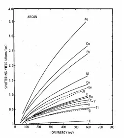
Sputter yield is given as the mean number of atoms remitted from a target per incident ion. The mass and energy of the incident atoms, angle of incidence, mass of target atoms, and target crystallinity will all affect the rate by which material is sputtered30. Thornton investigated the sputter yield of most commonly sputtered elements as a function of ion energy, which is provided as a quick reference guide30.
1.4 References
1K. Reichelt, Vacuum, v. 38, p. 1083, 1988.
2C. P. Constable, J. Yarwood, and W. D. Münz, Surface and Coating Technology, v. 116, p. 155, 1999.
3W. D. Sproul, Thin Solid Films, v. 107, p. 141, 1983.
4G. V. Samsonov, Soviet Physics-Technical Physics, v. 1, p. 695, 1967.
5P. Panjan, B. Navinšek, A. Cvelbar, A. Zalar, and I. Milošev, Thin Solid Films, v. 298, p.281, 1996
6K. Schwarz, A. R. Williams, J. J. Cuomo, J. H. E. Harper, and H. T. G. Hentzell, Phys. Rev. B, v. 32(12), p. 8312, 1985.
7L. E. Toth, Transition Metal Carbides and Nitrides, Academic, New York, 1971.
8I. Milošev, H. H. Strehblow, and B. Navinšek, Thin Solid Films, v. 303, p. 246, 1997.
9L. Krusin-Elbaum, M. Wittmer, C. –Y. Ting, and J. J. Cuomo, Thin Solid Films, v. 104, p. 81, 1983.
10M. Östling, S. Nygren, C. S. Petersson, H. Norström, P. Wiklund, R. Buchta, H. –O. Blom, and S. Berg, J. Vac. Sci. Technol. A, v. 2, p. 281, 1984.
11N. Kumar, K. Pourrezaei, B. Lee, and E. C. Douglas, Thin Solid Films, v. 164, p. 417, 1988.
12M. Y. Kwak, D. H. Shin, T. W. Kang, and S. Kim, Thin Solid Films, v. 339, p. 290, 1999.
13J. P. Noël, D. C. Houghton, G. Este, F. R. Shepherd, and H. Plattner, J. Vac. Sci. Technol. A, v. 2(2), p. 284, 1984.
14M. –S. Wong, G. –Y. Hsiao, and S. –Y. Yang, Surface and Coatings Technology, v. 133-134, p. 160, 2000.
15M. Setoyama, M. Irie, H. Ohara, M. Tsujioka, Y. Takeda, T. Nomura, and N. Kitagawa, Thin Solid Films, v. 341, p. 126, 1999.
17S. Ruvimov, Z. Lilental-Weber, J. Washburn, K. J. Duxstad, E. E. Haller, Z. R. Fan, S. N. Mohammad, W. Kim, A. E. Botchkarev, and H. Morkoç. Appl. Phys. Lett., v. 69, p. 1556, 1996.
18K. Schwarz, A. R. Williams, J. J. Cuomo, J. H. E. Harper, and H. T. G. Hentzell, Phys. Rev. B, v. 32(12), p. 8312, 1985.
19T. Yotsuya, M. Yoshitake, and T. Kodama, Cryogenics, v. 37, p. 817, 1997.
20R.G. Gordon, Mat. Res. Soc. Symp. Proc., v. 335, p. 9, 1994.
21B. O. Johansson, J. –E. Sundgren, J. E. Greene, A. Rockett, and S. A. Barnett, J. Vac. Sci. Technol. A, v. 3, pg. 303, 1985.
22J. Ito et al., United States Patent #6,426,512, issued 2002.
23B. Chapman, Glow Discharge Processes, John Wiley & Sons, Inc., New York, p. 177, 1980.
24K. Wasa and S. Hayakawa, Handbook of Sputter Deposition Technology: Principles, Technology and Applications, Noyes, New Jersey, 1992.
25R. A. Powell and S. M. Rossnagel, Thin Films: PVD for Microelectronics: Sputter Deposition Applied to Semiconductor Manufacturing, Academic Press, San Diego, 1999.
26D. M. Mattox, The History of Vacuum Coating Technology, 2002, from http://www.svc.org.
27F. F. Chen, Introduction to Plasma Physics and Controlled Fusion, Plenum Press, New York, 1984.
28http://my.engr.ucdavis.edu/~das/ctix/plasma.html
29J. R. Roth, Industrial Plasma Engineering: Principles, Institute of Physics Publishing, London, 1995.
30J. A. Thornton, Deposition Technologies for Films and Coatings: Development and Applications, ed. R. F. Bunshah, Noyes Publications, NJ, 1982.
32Thesis, NC State University, N. M. Williams, Enhanced Reactive Magnetron Sputtering of Aluminum Nitride, 1998.
33S. M. Rossnagel, Thin Films Processes II, ed. J. L. Vossen, W. Kern, Academic Press, New York, 1991.
34P. Sigmund, Topics in Applied Physics: Sputtering by Particle Bombardment I, ed. R. Behrisch, v. 47, Springer-Verlag, Berlin, 1981.
35G. K. Wehner, G. S. Anderson, Vacuum Technology, Thin Films, and Sputtering: an Introduction, ed. R. V. Stuart, Academic Press, New York, 1983.
36D. L. Smith, Thin-Film Deposition: Principles and Practice, McGraw-Hill, New York, 1995.
37J. Floro, C. Jahnes, and D. J. Mikalsen, Vacuum Technology, Laboratory Procedures and Deposition Processes, T. J. Watson Research Center, NY, 1986.
38W. D. Westwood, Progress in Surface Science, v. 7, p. 71, 1976.
39L. Hultman, Growth of Single- and Polycrystalline TiN and ZrN Thin Films by Reactive Sputtering; Influence of Low Energy Ion Irradiation, Thesis, Linköping University, Sweden, 1988.
40A. G. Dirks, H. J. Leamy, Thin Solid Films, v. 47, p. 219, 1977.
41D. W. Pashley, Epitaxial Growth: Part A, ed. J. W. Matthews, Academic Press, New York, 1975.
42S. A. Barnett, L. Hultman, J. –E. Sundgren, Appl. Phys. Lett., v. 53, p. 400, 1988.
43http://www.nitronex.com
44M. S. Wong, W. D. Sproul, X. Chu, and S. A. Barnett, J. Vac. Sci. Technol. A, v. 11, pg. 1528, 1993.
45S. Adachi and M. Takahashi, J. Appl. Phys., v. 87, pg. 1264, 2000.
46C. Carney and D. Durham, J. Vac. Sci. Technol. A, v. 17, pg. 2850, 1999.
47F. Englemark, G. Fucntes, I. V. Katardjiev, A. Harsta, U. Smith, and S. Berg, J. Vac. Sci. Technol. A, v. 18, pg. 1609, 2000.
2.0 EXPERIMENTAL STRUCTURE
The physical vapor deposition sputtering systems utilized for deposition of ZrN and GaN include a dual and a single source magnetron sputter system. Both systems were assembled at the Center for Advanced Manufacturing Processes and Materials and are unique to this research environment. The mechanisms for thin film deposition are different for each system and will be individually discussed.
2.1 Dual Magnetron
The dual magnetron system seen in figure 2.1 consists of four main components: the deposition chamber, pumping system, pressure monitor and control, and power supplies.
H20 in H20 out
Bias
N S N
H20 in H20 out
Plasma
Baratron gauge Convectron gauge
N S N
Cryogenic Pump
Power
Substrate Heater Substrate
Mass Flow Controller
Array (Ar, N2)
Nude Ion Gauge
Convectron Gauge
Nude Ion Gauge
Gate Valve
The deposition chamber is a 50 liter stainless steel vacuum chamber, which can either be heated or cooled by external heating and cooling jackets. Two six-inch diameter magnetrons are mounted face down and are isolated from the top plate. The targets can be biased by DC, RF, or AC biasing voltage. A six inch linear-motion mobile substrate holder is mounted at a distance of three inches below the targets and can be heated or cooled. The substrate holder is equipped with external bias capability.
The pumping system consists of an Edwards QDP40 Drystar vacuum pump used to evacuate the chamber to a pressure of 10-2 Torr (1.3 Pa.). A CTI Helix Technology Cryotorr10 cryogenic pump, with a pumping speed of 5,000 liters per second for argon, was used with a water-cooled CTI-Helix Technology 9600 He compressor to achieve a base pressure of 10-7 Torr (1.3 * 10-5 Pa.) for all depositions.
The pressure monitoring system consists of an MKS type 390HA-0001 capacitance manometer Baratron gauge with a range of 1 Torr and was used to monitor pressure during deposition. Both the chamber and the pumping system were monitored with a Granville-Phillips thermocouple Convectron gauge and a Troy-Onic, Inc. nude ionization gauge from Duniway Stockroom (Part # I-100-P), in conjunction with a Granville-Phillips 303 vacuum process controller. Two MKS Type 260 mass flow controllers, with a maximum flow of 100 sccm of nitrogen, were used to control the flow of argon and nitrogen to the system.
An Advanced Energy MDX Series Magnetron Drive direct current (DC) power supply was used for all DC experimentation. The MDX power supply is capable of supplying 10 kW in a constant current, voltage or power mode. An RFPP RF10S radio frequency power supply was used for capacitively-coupled experimentation. The RF10s operated at the standard 13.56 MHz with a maximum power output of 1000 W into a 50 ohm load. The RF10S can be pulsed with a specified frequency or operated in a constant operation mode.
Figure 2.2. CAMP-M dual magnetron sputter deposition system
2.2 Self Sputter Magnetron
Figure 2.3. Schematic self sputter magnetron deposition system.
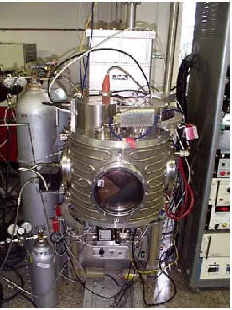
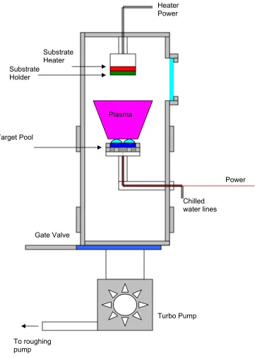
The deposition chamber is a 25 liter stainless steel vacuum chamber with a four inch quartz window sealed with a Viton® O-ring. A four inch water cooled target is mounted directly below the substrate. The substrate holder can be heated or cooled with target to
Turbo Pump
Power Substrate
Heater
Plasma
To roughing pump
Gate Valve
Chilled water lines Target Pool
Substrate Holder
substrate distance of 8 inches. The system is equipped with a hollow cathode emission source for increased ionization of gaseous species.
The pumping system is comprised of a Welch Duo-seal rotary vein pump used to evacuate the chamber to a pressure of 10-2 Torr (1.33 Pa.). A Leybold-Heraeus turbo pump was used to achieve a base pressure of 10-7 Torr (1.33 * 10-5 Pa.) for all depositions.
The pressure monitoring system consists of an MKS 122AA-00010AB capacitance manometer Baratron gauge with a range of 10 Torr and was used to monitor pressure during deposition. Both the chamber and the pumping system were monitored with Granville-Phillips thermocouple convectron gauges and an Electron Technology Inc. 4336K/1 nude ionization gauge with a Varian 843 vacuum ionization gauge. Two MKS Type 260 mass flow controllers with a maximum flow of 100 sccm nitrogen were used to control the flow of argon and nitrogen to the system. An ENI RPG-50 Pulsed DC power supply was primarily used for deposition.
2.3 Magnetrons
F. M. Penning was the first to propose and then patent1 magnetron sputtering in 19352. A prototype of the planar magnetron was invented by Wasa in 19672,3. Magnetrons utilize magnetic confinement of charged particles to increase ionization within regions close to the target. Such confinement allows for electron trapping within the magnetic field flux lines, but also allows ions to travel across the sheath and gain acceleration towards the target. Magnetrons are generally operated in a diode mode with rare earth magnets, such as barium ferrites, alnico alloys, cobalt-rare earth alloys4, or electro-magnets located behind the cathode in a circular or closed loop pattern as seen in Fig. 2.5.
Figure 2.5. Cross-section of a planar magnetron2.
The magnetic field is orientated parallel to the cathode surface such that the ExB drift path forms a closed loop5 in the shape of a toriod, or a “race track”. The generated ExB
field causes electrons to orbit along field lines confining primary and secondary electrons within this magnetic field loop. This increases the path length of the electrons thereby increasing the probability of an ionization event and increases the density of ionized species close to the cathode. The force upon an electron in a magnetic field is
→ →
× =qv B
Fm [2.1]
For particles moving perpendicular to this field, the force causes the particles to orbit with a radius, known as the Larmour radius, that is given by
qB m
where the perpendicular velocity is the component in the kinetic energy ½mυ2
⊥, and is equal to the potential energy by conservation; thus
qB kE m
r= 2 ( ) [2.3]
where m is the electron mass, k is the Boltzmans constant, E in the strength of the electric field, q is the elemental charge of an electron, and B is the strength of the magnetic field.
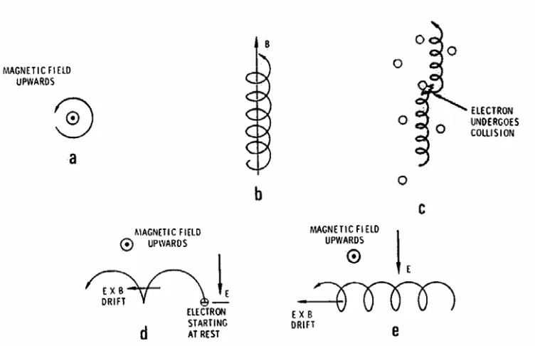
Figure 2.6 shows the effects of magnetic and electric fields on electron orbit. Fig 2.6a depicts an electron rotating around a magnetic field coming perpendicularly out of the page. 2.6b shows the electron orbital path along a magnetic field oriented parallel to the page. 2.6c shows a representation of electron impact and the impacts effect on an electron traveling along a magnetic field oriented parallel to the page. 2.6d and 2.6e show electron motion within an electric and magnetic field oriented perpendicular to one another. The electron will “drift” and orbit around the ExB direction under the influence of the magnetic and electric field.
Secondary electrons emitted from the target become trapped within the magnetic toriod and are confined to this closed loop. An increase in the number of the active species close to the cathode results in an increased rate of deposition. The only limitation in the deposition rate of magnetron systems is the ability to cool the cathode4. Cathode cooling becomes an issue due to the high power dissipated at the cathode where 55%-70% of the applied power is lost to heating4. The high electron density in regions near the cathode results in a high current, low voltage discharge4. Due to increased plasma density, magnetron discharges can be sustained at lower operating pressures, which results in less gas scattering.
A wide variety of magnetrons have been developed in two basic geometrical groups: planar4 and cylindrical7. All magnetron sputtering geometries utilize a closed loop ExB
field for electron confinement.
2.3.1 Balanced versus Unbalanced Magnetron Sputtering
The magnetic field line arrangement in a magnetron discharge will have an effect upon the operation and properties of a plasma. A magnetron is said to be balanced when all of the field lines emanating from the north poles of the magnet arrangement are re-connected to the south poles of the exterior magnet as shown in figure 2.7.
Unbalanced magnetrons utilize an unmatched set of magnets such that the magnetic field lines bleed out to the substrate as seen in figure 2.8.
Figure 2.8. Unbalanced magnetron8.
Unbalanced magnetrons are advantageous for increasing the energy available at the substrate by channeling ions to the surface of the substrate, which increases ion bombardment of the substrate and will affect the properties of the growing film.
2.3.2 DC Magnetron Sputtering
Direct current (dc) sputtering has become a preferred method for metal deposition. Providing high deposition rates and uniform coverage, dc magnetron sputtering provides the ability to quickly deposit large amounts of material. A typical magnetron sputtering system can be seen in Fig.2.1. DC magnetron sputtering systems are typically operated in argon at cathode potentials from 300-700 V and pressures between 1-10 mTorr4. For ideal magnetic confinement, several researchers4,5 state that the voltage current characteristics follow
n
kV
I = [2.4]
(
)
3/2o V V C
I = − [2.5]
for magnetron discharges, where Vo is the minimum voltage at which the discharge can be maintained which governed by the Paschen law, and
(
1)
2 3/2 12 2L M e K
C ≈ +γ εo [2.6]
where M is the atomic weight of the sputtering ion, γ is the secondary electron coefficient, L is the distance of the dark space and K is a pressure dependent9. The cathode in dc sputtering is referred to as cold as it does not rely on the thermionic emission of secondary electrons to sustain the discharge10.
2.3.3 Pulsed DC Sputtering
DC sputtering is used primarily for the sputtering of conducting electrodes, which limits the process to the sputtering of metals and low resistivity metallic alloys. Pulsed DC sputtering is a relatively new method of sputter deposition. Pulsing the magnetron discharge in the mid frequency range (10-200 kHz) stabilizes the plasma, prevents arcing, and yields high quality insulating compounds11.
Figure 2.9. Pulsed dc waveform12.
The actual waveform for pulsed magnetron sputtering varies due to inherent characteristics of the plasma.
2.4 Plasma Characterization
2.4.1 Pressure Effects on I-V Characteristics
A Bell 640 Incremental guassmeter was used to measure the magnetic field strength across the surface of the dual magnetron target and at the surface of the substrate. The strength of the magnetic field arrangement is depicted in Figure 2.10.
Figure 2.10. Dual magnetron magnetic field arrangement.
N
350G S 900G N 350G
3 inches
10G 7G
7G
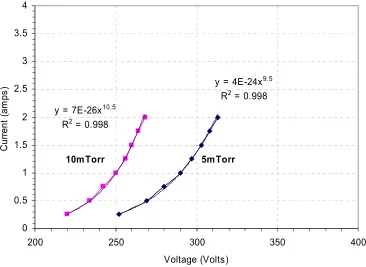
The dc magnetron plasma was characterized by examining the applied current-voltage characteristics to investigate the efficiency of electron trapping and the effect of deposition pressure on the electron trapping for the dual magnetron system. The Advanced Energy power supply was operated in constant current mode and current was incrementally adjusted from 0.25 to 2 amps with applied voltage read at each incremental step. The applied voltage was displayed by the Advanced Energy MDX magnetron power supply. The I-V characteristics measured at 5 and 10 mTorr can be seen in figure 2.11. As the operating pressure is increased the applied voltage is noticeably decreased for the same current. These measurements show that magnetron voltage will increase slowly even upon large changes in cathode current. Rossnagel6 shows this same effect for Cu, Al sputtering in argon that as gas pressure increases, gas density increase and the voltage required is reduced for the same current.
y = 4E-24x9.5
R2 = 0.998 y = 7E-26x10.5
R2 = 0.998
0 0.5 1 1.5 2 2.5 3 3.5 4
200 250 300 350 400
Voltage (Volts) C urre nt (a m ps ) 5mTorr 10mTorr
Figure 2.11 is designed to document the performance of the dual magnetron system and can be used a reference for power consumption determination during operation. For experimentation performed at 5 mTorr and 10 mTorr, the current/voltage characteristics can be calculated.
Power law trendlines were fit to the experimental data points for both experiments conducted and R2 values achieved were at least 0.998. The results show an extremely small value of k, and a fluctuation in n of 0.9 by doubling the pressure.
2.4.2 Langmuir Probe Characterization
An electric (Langmuir) probe was utilized to examine several plasma parameters. Electron temperature (Te), electron density (ne), ion density (ni), plasma and floating potential (Vp and Vf, respectively) and ion flux (Γi) were found from measurements taken with a Langmuir probe. The circuit of the Langmuir probe is shown in figure 2.12. The probe was constructed of a thin tungsten wire with a diameter of 0.24 mm, an exposed length of 6.64 mm, and a cross-sectional area of 5.052 * 10-6 m2. Measurements were taken during sputtering with mixtures of argon and nitrogen gases.
Figure 2.12. Circuitry schematics of CAMP-M Langmuir probe.
The electric probe technique was developed by Langmuir as early as 192413. An electric probe is a thin electrode, typically a wire, connected to an ammeter, voltmeter
A V
Single Probe Configuration Double Probe Configuration
and power supply capable of biasing the probe positively or negatively. When inserted into a plasma, the current the probe collects as a function of applied voltage is then used to gather information about the condition of the plasma. The advantage of this technique is that localized measurements can be made, where other techniques give average information over a large volume. When the probe is biased positively, negative charge is collected until saturation occurs. As the negative charge carriers are typically electrons, this portion of the I-V curve is referred to as electron saturation. When the probe is biased negatively, positive charge carriers are collected until saturation is reached. As the positive charge carriers are ions, this portion of the I-V curve is referred to as ion saturation.
The Langmuir probe, while relatively simple in design, is an effective means for determining plasma parameters. Electron probes provide a means for determining plasma parameters with little disturbance of the plasma. Any disturbance within a plasma is localized by the plasma and will not affect the overall behavior.
While there is some error associated with the use of Langmuir probes, they are useful for a relatively inexpensive method of quickly characterizing plasmas.
2.4.2.1 Single Probe
Figure 2.13. Typical single Langmuir probe I-V curve14.
From evaluation of the curve the electron temperature (Te) can be calculated from
e
kT e dV
I dln| |=
[2.7]
where k is the Boltzmann constant, and e is the electron charge. Thus, for a log plot, the slope dV/d(lnI) is a measure of the plasma electron temperature:
) (lnI d dV k e
Te = [2.8]
From electron and ion saturation currents, electron and ion density can be found from
2 1 8 4 1 = e e e e m kT A en I
π [2.9]
2 1 = i e i i m kT A en
I [2.10]
This technique is valid when the probe radius is large compared to the sheath distance given by the Debye length
2 / 1 2
4
= ne kTe D π
Using a technique suggested by Dr. Bourham, the floating potential can be used to calculate electron temperature through
2 / 1 4 ln − = e i e f m m e kT V
π [2.12]
The ion density can then be calculated through
+ ≅ m kT eA I n e p i i 7 . 1 [2.13]
The ionization fraction can then be found by calculating the ratio of ion density to total number of particles.
-0.5 0 0.5 1 1.5 2 2.5
-30 -20 -10 0 10 20
Voltage (V)
C
urren
t (m
ic
ro
A
)
Figure 2.14. Single probe measurement of dc zirconium sputtering at 0.5 amps, 5 mTorr at the substrate center.
Table 2.1. Electron temperature and ion density at 0.5 ampere.
0.5 Ampere
Te (eV) Ii (m-3)3 mTorr 2.18 8.29*1017
5 mTorr 1.94 8.29*1017
7 mTorr 1.62 8.96*1017
Table 2.2. Electron temperature and ion density at 1.0 ampere.
1.0 Ampere
Te(eV) Ii(m-3)3 mTorr 1.94 1.4*1018
5 mTorr 1.78 1.37*1018
Ion density, ion current and ionization fraction were found to increase with cathode current. Ion density, ion current and ionization fraction were found to decrease with pressure. The Debye length was calculated and found to be much smaller than the probe diameter, validating the use of the equations. As cathode current increases, the density of ionized species increase, and the number of those transferred to the substrate are also increased. As pressure is increased, the mean free path, the average distance a particle can travel, is decreased. This decrease in mean free path reduces the energy of ions arriving at the substrate. The mean free path is calculated from
P N d RT MFP A 2 2π
= [2.14]
where R is the gas constant, T is temperature, d is particle diameter, NA is Avogadro’s number and P is pressure. The MFP decreases from 6 cm. to 1.5 cm. when pressure is increased from 5 mTorr to 20 mTorr.
2.4.2.2 Double Langmuir Probe
The double probe technique uses two identical probes, one to draw electron current and one to draw ion current. The two together, however, draw no net current. Double probes are used to quickly determine electron temperature (Te) from
e i V T i dV dI 2 0 = = [2.15]
Figure 2.15. Typical double Langmuir probe characteristics13.
Double probe measurements were taken during reactive magnetron sputtering of zirconium in argon and nitrogen. The double probe was located at the center of the substrate for all measurements. The sputtering pressure was 5 mTorr and the cathode current was 0.5 amperes. A plot of the current versus applied voltage can be seen in figure 2.16.
-8 -6 -4 -2 0 2 4 6 8
-60 -40 -20 0 20 40 60
Voltage (V)
C
urre
nt
(m
ic
ro
-A
)
4% N
100% N
Electron temperature can be determined from double probe evaluation by examining the slope of the curve through zero as
e
kT
Slope= 1 [2.16]
or estimated from the voltage difference between the “knees”
4
∆ = e
T [2.17]
Utilizing electron temperature, electron density can be calculated
2 1 2 4 . 0 − ≈ i e p p e m kT eA i
n [2.18]
where Ap is the area of the probe, mi is ion mass, and ip is probe current and assuming a quasi-neutral plasma ne≈ ni, the ion flux can be calculated from
2 1 = = Γ i e i i i i m kT n
nυ [2.19]
and υi is the Bohm velocity (kTe/mi)1/2.
The data obtained from double probe experimentation for the deposition of ZrN (4% N2) and Zr3N4 (100% N2) and equations 2.16-2.18 is summarized in table 2.3.
Table 2.3. Double probe characterization results.
It was found that the sputtering of higher ZrN resulted in a slightly lower electron temperature, with little to no change in electron density. It was found that there was negligible change in Te upon change in nitrogen concentration from 4 to 100%.
4% N2 100% N2
Te 3.18 eV 3.11 eV
The difference noted between single and double probe measurements is due to the method of collection. The single probe is biased with respect to ground and collects the true current which is directly related to charge carrier density and electron temperature. The double probe is floating and collects only circuit current. The error in density measurements of the double probe may as high as 40-50%, but is a useful technique for quickly determining electron temperature.
2.5 Thin Film Characterization
Sheet resistance (Rs) was measured utilizing a four point probe apparatus comprised of Keithley 224 programmable current source, HP 3456A digital voltmeter and a Signatone four point probe. The probe injects current from two electrodes across the film with two other electrodes measuring the voltage collected as seen in the figure 2.17.
Figure 2.17. Schematic of four point probe set up.
If the spacing of the probes is constant and the edges of the sample are more than four times this distance away from the measurement sight, sheet resistance (Rs) can be found from
s s s
I V
R =4.532∗ [2.20]
which is the two dimensional sheet resistance (Ω/ ) and is the resistance between two electrodes on opposite sides of a theoretical square16. Is is the current injected and Vs is
the voltage measured. Film thickness (d) and resistivity (ρ) are related to sheet resistance (Rs) through.
d
Rs = ρ [2.21]
Therefore, if the thickness of the film is known, and the sheet resistance has been measured, the resistivity can be calculated.
All of the film thicknesses presented were measured with a Dektac 3030 profilometer from silicon samples that had been partially masked during deposition to create a step. The reported accumulation rates were calculated from these measurements. Profilometer scans were run three times and an average thickness was obtained.
Thin film crystal orientation was measured with a Rigaku diffractometer using Cu Kα radiation (λ = 1.543 Å). θ-2θ scans were performed in order to determine the orientation of the films. A Hitachi S-3200N environmental scanning electron microscope was used to examine the structure of several of the films. Accelerating voltages were between 10 to 25 keV. A Topcon transmission electron microscope (TEM) was utilized to obtain high resolution TEM images of atomic structure
2.5.1 Raman Spectroscopy17
Crystals can be thought of as a group of balls connected by springs, which can vibrate with a frequency dependent upon the mass of the balls and the strength of the springs. Diatomic molecules (two balls/one spring) have only one fundamental vibrational frequency. These vibrational frequencies are high, 1012-1014 Hz, or the infrared region. The Raman spectrum comes from the indirect coupling of high-frequency radiation with the electrons that make up the chemical bond. Therefore, Raman spectroscopy is sensitive to atomic arrangement and chemical bonding, but is used primarily for structural characterization, because it is more sensitive to bonding than chemical composition.
energy is reradiated. Rayleigh scattering occurs when energy is given off at the same frequency as the incident light. A small portion of this energy is transferred to the sample and is said to excite the vibrational modes. The separation of the Raman lines from the Rayleigh line is a direct measure of the vibrational frequencies of the sample. The Raman process that excites molecular and crystal vibrations is called Stokes scattering, and the process that annihilates existing vibrations is known as anti-Stokes scattering. The anti-Stokes scattering depends upon existing thermal vibrations and is highly temperature dependent. Thus, anti-Stokes scattering is rarely measured, and it is the Stokes intensities that are typically measured as they are only weakly temperature dependent. Figure 2.18 shows a typical spectrum obtained from Raman analysis.
Figure 2.18. Typical Raman spectroscopy plot17.
2.6 Gallium Nitride
Gallium nitride (GaN) was first reported by Johnson et al. in 1928 and was referred to as “Gallic nitride”20. Gallium nitride is member of the III-V semi-conductors family that consists of three commercially valuable materials and their alloys, for device applications: AlN, GaN, and InN. GaN is a direct wide band gap semiconductor that is today finding uses in blue and UV light emitters and detectors, secure space communications, and is currently being investigated for short wavelength laser applications20. It has been found that Schottky barriers on GaN have barrier heights depending upon the difference in work function between the contact and GaN21. A metal with a work function less than that of GaN will yield an ohmic contact and a higher work function will yield a rectifying contact21. GaN is slated to be the substrate of choice for the future high temperature, high power, high frequency devices21. Methods of film deposition include molecular beam epitaxy (MBE)22,23,24, chemical vapor deposition (CVD)25,26, reactive sputtering27,28, pulsed laser deposition (PLD)29,30,31, metal-organic chemical vapor deposition (MOCVD), high vapor phase epitaxy (HVPE)32,33.
The III-V semiconductors form a continuous alloy system capable of generating light from the red to UV.20,29 GaN has a thermal conductivity (κ) of 1.3 W/cm K, a dielectric constant of 9.5, a band gap (Eg) of 3.4 eV20. GaN lattice constants and thermal expansion information can be found in table 2.4.
Table 2.4. Gallium nitride material properties.20
Lattice spacing Coefficient of thermal
expansion (α)
a: 3.189Å 5.59 * 10-6/K
c: 5.185Å 3.17 * 10-6/K
reduced heat generation of LED’s allows them to replace traditional tungsten bulbs in application. The most noticeable of which is in stoplights across the nation.
2.6.1 Lattice and Thermal Expansion Mismatch
Gallium nitride (GaN) grown as thin films suffers from a lack of suitably lattice and thermally matched substrates. Buffer layers of aluminum nitride (AlN), zinc oxide (ZnO) have been investigated34,35,36 to reduce the mismatch. Substrates of silicon carbide (SiC), gallium arsenide (GaAs), and sapphire are also widely used37,38,39,40. Sapphire is currently the substrate of choice since it is widely available in larger wafer sizes, is thermally stable, has a hexagonal crystal structure, is easily cleaned and relatively inexpensive. Large thermal and lattice mismatches between substrate and film often result in strained GaN films with large defect densities41. The high cost of these substrates, with respect to silicon, has pushed many research groups to attempt to develop methods to grow high quality GaN films using silicon substrates29,42,43,44,45,46,47,48.
Table 2.5 summarizes lattice mismatch between several substrates/buffer layers and GaN thin films. Mismatch calculations were performed using equation 2.21 given by Pashley49 who states that epitaxial growth occurs when the lattice mismatch between substrate and film is less than 15%. The relation is obtained through
Lattice Mismatch *100
− =
s f s
a a a
[2.22]
Table 2.5. Lattice mismatch between substrate materials/buffer layers to gallium nitride.
Substrate/
Buffer layer Structure
a – axis (Å)
(111) spacing (Å)
GaN % mismatch a
AlN Wurtzite 3.11(20) N/A 2.5
GaAs Cubic 5.65(20) 4.00 20.3
6H-SiC Hexagonal 3.08(20) N/A 3.5
Sapphire (0001) Corundum 4.75(20) N/A 13.54
ZnO Wurtzite 3.25(20) N/A 1.88
Silicon Diamond Cubic 5.43(20) 3.84 17.0
ZrN NaCl 4.58(54) 3.24 1.57
The lattice mismatch between sapphire and gallium nitride is 13.54%, between silicon and GaN is 17%. Silicon with a (111) orientation has been investigated as an epitaxial substrate50,51. The thermal expansion coefficient of silicon, sapphire and ZrN are shown in Table 2.6
Substrate Thermal Expansion Coefficient
Silicon 2.33 * 10-6/°C(52) Sapphire 7.50 * 10-6/°C(53) ZrN 7.24 * 10-6/°C(54)
2.7 References
1United States Patent # 2,146,025
2K. Wasa and S. Hayakawa, Handbook of Sputter Deposition Technology: Principles, Technology and Applications, Noyes, New Jersey, 1992.
3K. Wasa and S. Hayakawa, Review of Scientific Instruments, v. 40, p. 693, 1969.
4R. K. Waits, J. Vac. Sci. Technol., v. 15, p.179, 1978.
5S. M. Rossnagel, Handbook of Plasma Processing Technology: Fundamentals, Etching, Deposition, and Surface Interactions, ed. S. M. Rossnagel, J. J. Cuomo, W. D. Westwood, Noyes, New Jersey, 1992.
6J. A. Thornton, Deposition Technologies for Films and Coatings: Development and Applications, ed. R. F. Bunshah, Noyes Publications, NJ, 1982.
7J. A. Thornton, J. Vac. Sci. Technol., v. 15, pg. 171, 1978.
8D. L. Smith, Thin-Film Deposition: Principles and Practice, McGraw-Hill Inc., New York, 1995.
9W. D. Westwood, S. Maniv, and P. J. Scanlon, J. Appl. Phys., v. 54, p. 6841, 1983.
10J. R. Roth, Industrial Plasma Engineering: Principles, Institute of Physics Publishing, London, 1995.
11P. J. Kelly and R. D. Arnell, Vacuum, v. 56, p. 159, 2000.
12P. J. Kelly, P. S. Henderson, and R. D. Arnell, G. A. Roche, D. Carter, J. Vac. Sci. Technol. A, v. 18, p. 2890, 2000.
13F. Chen, Plasma Diagnostic Techniques, ed. R. H. Huddlestone, S. L. Leonard, Academic Press, New York, 1965.
14L. Schott, American Vacuum Society Classics: Plasma Diagnostics, ed. W. Lochte-Holtgreven, AIP Press, New York, 1995.
15J. W. Cho, unpublished results.
16http://four-point-probes.com/short.html