University of Windsor
University of Windsor
Scholarship at UWindsor
Scholarship at UWindsor
Electronic Theses and Dissertations
Theses, Dissertations, and Major Papers
8-13-1966
Synthesis of a digital computer controlled optimal and adaptive
Synthesis of a digital computer controlled optimal and adaptive
control system.
control system.
Adam Baziw
University of WindsorFollow this and additional works at: https://scholar.uwindsor.ca/etd
Recommended Citation
Recommended Citation
Baziw, Adam, "Synthesis of a digital computer controlled optimal and adaptive control system." (1966). Electronic Theses and Dissertations. 6413.
https://scholar.uwindsor.ca/etd/6413
This online database contains the full-text of PhD dissertations and Masters’ theses of University of Windsor students from 1954 forward. These documents are made available for personal study and research purposes only, in accordance with the Canadian Copyright Act and the Creative Commons license—CC BY-NC-ND (Attribution, Non-Commercial, No Derivative Works). Under this license, works must always be attributed to the copyright holder (original author), cannot be used for any commercial purposes, and may not be altered. Any other use would require the permission of the copyright holder. Students may inquire about withdrawing their dissertation and/or thesis from this database. For additional inquiries, please contact the repository administrator via email
SYNTHESIS OF A DIGITAL COMPUTER CONTROLLED OPTIMAL AND ADAPTIVE CONTROL SYSTEM
by Adam Baziw
A Thesis
Submitted to the Faculty of Graduate Studies Through the Department of Electrical Engineering in Partial Fulfillment
of the Requirements for the Degree of Master of Applied Science at
University of Windsor
UMI Number: EC52594
INFORMATION TO USERS
The quality of this reproduction is dependent upon the quality of the copy
submitted. Broken or indistinct print, colored or poor quality illustrations and
photographs, print bleed-through, substandard margins, and improper
alignment can adversely affect reproduction.
In the unlikely event that the author did not send a complete manuscript
and there are missing pages, these will be noted. Also, if unauthorized
copyright material had to be removed, a note will indicate the deletion.
®
UMI
UMI Microform EC52594
Copyright 2008 by ProQuest LLC.
All rights reserved. This microform edition is protected against
unauthorized copying under Title 17, United States Code.
ProQuest LLC
789 E. Eisenhower Parkway
PO Box 1346
Ann Arbor, Ml 48106-1346
This thesis of Adam Baziw is approved:
University of Windsor
September 1966
ABSTRACT
This thesis describes the synthesis of a novel digital method for optimization and adaption of certain second order systems which may be represented in the phase plane.
A digital controller had been partially constructed when the project was begun, therefore, only details of the modifications and additions to the controller are given in this report.
The plant includes a large load mass to approximate a pure inertia system. It is believed that the method of applying control to the
armature of a d.c. motor is novel.
In the control scheme, the optimal switching curve is stored in memory at the locations given by the velocity which is approximated by a difference of error readings over a constant sampling time. A new optimal switching curve is continually stored during each control cycle.
The program was written with the limited number of instruction steps, possible on the controller, in mind. It was found that the program could not be accommodated on the present controller. To carry out meaningful studies, the controller must be expanded or a controller with greater input and memory facilities used.
iii
ACKNOWLEDGEMENTS
The author wishes to express his appreciation to Dr. P. A. V. Thomas
who supervised this project and gave many helpful suggestions during its
course.
T A B L E O F C O N TEN TS
ABSTRACT
I . INTRODUCTION 1
A. Control Scheme 2
B. The Digital Control Computer 5
II. CALCULATIONS OF THE OPTIMAL SWITCHING CHARACTERISTICS 7
A. Physical Problem Considered 7
B. Calculation of the Optimal Switching Characteristic 9
1. Optimal Switching Characteristic for the Plant 10 K'/s(s+a)
C. Optimal Switching Characteristics for Additional Second 13 Order Plants
1. The Double Integral Plant G(s) = K ?/s^ 13
2. Optimal Switching Characteristic for a Plant 14 with Two Time Constants K'/ (s+a)(s+b)
3. Optimal Switching Characteristic for the Harmonic 15 Oscillator, K ’/fs^+cu^)
4. Optimal Switching Characteristic for a Second Order 16 Nonlinear Plant
D. Analysis of Control Relay Dead-Time 17
2
1. Effect of 6^ and 6^ for the Plant K/s 19 2. Effect of 6^ and 6^ for the Plant K/s(s+a) 21
III. DIGITAL CONTROL COMPUTER MODIFICATIONS 23
A. Phase Counter 24
B. Multiplication Unit 25
C. Delay Line Memory 27
D. Gating of Accumulator 28
E. Accumulator 29
V
TABLE OF CONTENTS (Continued)
III. DIGITAL CONTROL COMPUTER MODIFICATIONS (Continued)
F. Right and Left Shifting the Accumulator 32
G. I-Registers 34
H. Inversion Gating 35
I. Adder/Subtractor 35
J. Bit Counter and Timing Unit 37
K. (Control) N-Register 39
L. Compare Unit 40
M. Word Counter 41
N. Location Encoder 42
0. Increase I.C. Gating 43
P. Jump/Test Logic and Instruction Counter 44
IV. DESCRIPTION OF HARDWARE 46
A. General Description 46
B. Input 47
C. Output 48
1. Logic 48
2. Relays 50
3. Contact Protection 51
V. EXTENSION TO HIGHER ORDER SYSTEMS 52
A. Optimal Switching Characteristic for the Plant K/s^ 52 B. Control Surface for the Plant K/s^(s+a), |u|<1 54
C. Control Hypersurfaces for Plants With N Real Poles 57
TABLE OF CONTENTS (Continued)
VI. RESULTS AND DISCUSSION 58
A. Description of Computer Program 58
1. Determination of Initial Control and Input 58
2. Relay Compensation and Compare Modes 60
3. Store Mode 61
B. Control Computer Program 63
C. Discussion 66
APPENDIX A: Motor Transfer Function APPENDIX B: Control Computer Functions
REFERENCES
vii
1 INTRODUCTION
The main purpose of this study is to describe the synthesis of a control scheme which was proposed in a previous study ll]. However, some
of the statements made in the previous study might lead us to believe that the control scheme proposed there, and synthesized here, is more
general than it actually is.
In reference I, we are told that,"The study proposes a digital computer controller (DCC) method of optimization and adaption of systems representable in the phase plane". Actually the system proposed there, when suitably modified, is more accurately described as follows: "A
digital computer controller is proposed for second order systems which can have varying parameters, but the variations must be slow compared to
the shorter "control periods, so that, for a particular control period, we may assume that the plant has constant coefficients. Furthermore, the
two "poles"* of the second order system must always be real-valued. The system is optimal in the sense that the desired state of the controlled variables (position and velocity) is reached in minimum time, with amp
litude constraints on the controlling function. The control scheme is adaptive in the sense that the controller adjusts itself to slowly vary
ing parameters of the system". This modified statement shall be justified
* By "c o n t r o l p e r i o d " w e m e a n o n e cycle of the control operation. Thus, once the controller "locks" onto the optimal switching curve, it is able to satisfactorily follow this curve, which of course changes as the
parameters of the system being controlled.
on a theoritical basis in the following sections.
Most of the analysis for the problem we are considering has been done in the 1950's, for example, Refs. 2,3,4,5,6.
A. Control Scheme
The control scheme applied in this study [l] is applicable to a
certain class of second order systems (plants); in particular, those plants which have an optimal switching characteristic (OSC) which is of the form shown in Figs. 1-1 and 1-2. To be more precise, Fig. 1-2 is used to define certain regions of the phase plane. Using the symbols in Ref. 7, where much of this section is covered, we see in Fig. 1-1 that u=+l for (xj,X2) € R + U 7+> and that u=-l for (x^,X2) € RJJ
In order to describe clearly the control scheme which is used, phase trajectories typical of the class of systems being considered, are
shown in Fig. 1-2. The solid lines are the phase trajectories for the Legend
7- curve is the locus of all points which can be forced to the origin by the cont
rol u=-l.
7+ curve is the locus of all points which can be forced to the origin by the cont
rol u=+l.
7 is the optimal switching characteristic and is given by =7+ U 7_.
R_ is the set of all points to the right of
R + is t h e s e t o f a l l p o i n t s t o t h e l e f t o f 1
u = - 1
R_
The O p tim a l S w itchin g C h a r a c t e r is t ic 7
-1
-Fig. 1-1 The optimal switching characteristic typical of plants considered in this study.
^ The symbol All B means the union of the two sets of points A,B, and the symbol (xj,X2) € C means the point (x^,X2) is a member of the set C.
3
control u=H-l, while the dashed lines are the phase trajectories for
u=-l.
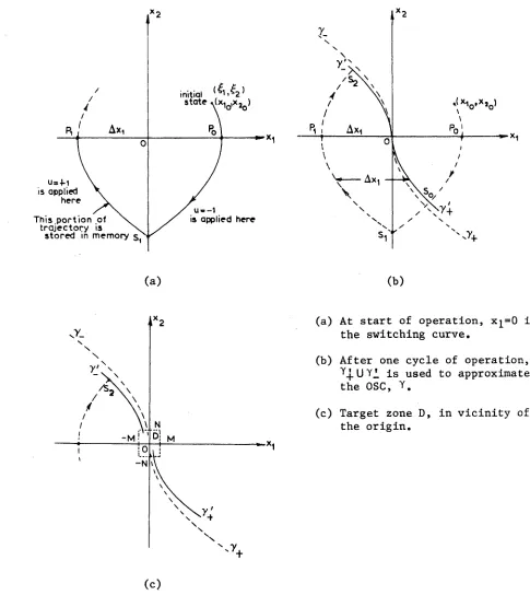
Next the control scheme used in this study is described. Referring
to Fig. 1-3, consider an initial point in the phase plane (xio>x 2())* Without any previous knowledge of the systems switching characteristic Y, the X2-axis is used as a switching
curve. Thus, if xj^O, we apply the
control u=~l, and if x^<0 we apply the control u=+l. At Sj^ (x^=0), the
control is switched from u=-l to u=+l. From Si to Pj (x2=0), this portion of the trajectory is stored in the memory of the computer. It is noted that the
trajectory from Pq (x2=0,x i>0) to Sj is not stored. During this portion of the trajectory, the values of xj are compared with values of xi in the memory at the addresses given by the corresponding value of X2- During the first pass, these values are zero. Now the assumption is made that the curve from Si to Pi is similar to ^+, so if Si'Pi is shifted to the right by the distance Axi, then a portion of
Y+ will have been approximated. Next, it is assumed that Y_=-'V’+ (which is the same as assuming that the optimal switching characteristic Y is an
odd function). We denote the approximating trajectories to Y by Y 1, so that, Y'=y4.UyI. No w if the points along the trajectory from Pi to S2
are compared to the corresponding points along YL (i.e., for the same
value of X2) and the control switched from u=+l to u=-l when the two Fig. 1-2 Typical phase trajectories
4
initial
u= 4 -1
is applied h e re
u » - l
is applied h ere
T h is p o r t io n o f \
t r a j e c t o r y is s to r e d in m e m o ry
>s
(a) (b)
- N
(a) At start of operation, x^=0 is the switching curve.
(b) After one cycle of operation, Y_j.UYi is used to approximate the OSC, Y.
(c) Target zone D, in vicinity of the origin.
(c)
Fig. 1-3 Schematic of the Proposed Control Scheme
curves intersect, the system will move along the Y.1 curve toward the
origin.
In an actual system, it is practically impossible to reach the
5
origin exactly. However, if a region D is specified by
D = { (x-^ ,X2 ) ; -M<x^<M, - N < X2<N}
where M and N are prespecified constants depending on the accuracy
requirement of the system, then, the desired final state will have been reached when (x^,X2)£D. If the system misses or overshoots region D,
the logic will sense the error and switch again towardY1 •
At this first time the system is not time optimal. If the system
parameters do not change, the system will move to the origin with only one switch [i.e., at Sq if ( x ^ , X2^) is in region R_ or at S2 if
(x^q,X2q) is in region R+Jand the system will be essentially time optimal.
B . The Digital Control Computer
In 1963, before an actual control scheme for any particular pro blem had been proposed, the Electrical Engineering Department at the University of Windsor began developing a digital control computer [8]. At the time, the design was to "incorporate into this computer the de
sired flexibility. This flexibility would include an extensive list of
instructions, a suitable means of data storage, and special input and
output facilities".^
The computer uses NAND logic throughout, and the digits ZERO and ONE are represented by voltage levels, 0 volts and -6 volts, respectively
[
10].
The sign of the binary number is denoted by the most significant digit of the 12 bit word: ZERO and ONE represent the positive and neg ative signs, respectively. For positive numbers, the number digits
*f*
6
represent the magnitude, while for negative numbers the number digits are
in 2 fs complement. The signed 2's complement representation of a
binary number gives the actual value of the binary number if the value of the sign digit is regarded as a negative number [9]. By considering a decimal point after the sign digit the number system is :
0.00000000000 to 0.01111111111 (0*x<V4) 1.10000000000 to 1.11111111111 (-'/2<x<0) so that any number is represented by a fraction.
II. CALCULATIONS OF THE OPTIMAL SWITCHING CHARACTERISTIC
A. Physical Problem Considered
In this study we consider applying the control scheme to an armature
Relays M o to r Load r ~
dc
(a) plant
geqr ra tio A m plifier M o to r Load
Controller
/ f (x,x)
(b) system
Fig. 2-1 Schematic Diagram of the physical problem considered.
controlled d.c. motor. The quantity to be controlled is the output angle (or position)0 of a Shaft Encoder, which is coupled by gears to the motor shaft. A schematic representation of the problem is shown in Fig. 2-1.
In Fig. 2-1, AjJ^Ct) ,B;L,(t) are the voltage gain, load inertia and load damping coefficients, respectively. The torque due to the load is
tl = bl (t) 0 + d _ [ J L (t)e] dt
8
Next, as pointed out in the Introduction, A,B^(t) and JL(t) are
assumed to be essentially constant for the relatively short control periods.
Now, let J^j(t) and Bj^(t) be the inertia and viscous damping of the motor. These quantities are not known in general, but are assumed to vary only
slightly for a particular control period. Then, dropping t from the terms, we may let
J - JL + JM
B = Bl+ Bm (2-2)
In appendix A, the transfer function of the motor is shown to be 8(s) = kT/ jM ________
Au(s) s + 1_ (BM + K4Kt) (2-3)
JM
For the motor and load the transfer function is 6(s) = KT/(JL + JM)
AU(S) s + (BL + BM + K 4Kt)
(JL + Jm) (2-4)
or 6(s) K"/J
u(s) s + B'/J (2- 5)
where K" = A
B ’ = Bl + Bn + K 4 Kt (2-6)
If J >> B*, then (2-5) becomes
9 (s) = r V J (2-7)
u(s) s
In any practical problem, we must consider constraints on the amount of control available. It is intuitively plausible that we could make u
(which is a voltage in this problem) arbitrarily large in order to drive the motor to the reference position in minimum time (the voltage on the coils of the motor would be a very large value for some time interval, and then a very large value of the opposite sign for the rest of the
time until x=0 and x=6ref, i.e., we accelerate the motor using very large voltages). Arbitrarily large voltages are very hard on the motor and
associated electronics, and would not be a desirable feature of the
speed control because the large accelerations would damage the controlled
object. So we can assume
ju'(t)| = |f(x,x)| ^ M, a known constant, (2-8)
Then we can summarize the problem as follows:
Given the physical system shown in Fig. 2.-1, having the mathematical
description of Eqns. (2-5) or (2-7), where the parameters of the system are as specified by Eqns. (2-2) and (2-6), find the control u(t) = f(x,x)
such that x = 0 and x ="0ref in minimum time, where the control is sub ject to the constraint
|u*(t) | = |f(x,x)| $ M, a known constant.
We write u ‘(t) = f’(x,x) to indicate that the control is to be based on
observing the velocity, 0, and the position, 0, of the motor (or load)
• •
multiplied by the gear ratio , n (a constant), i.e., x = n0 and x = n0.
B. Calculation of the Optimal Switching Characteristic
From the discussion in the previous section, we see that there is no loss in generality if we consider the two problems shown in Fig. 2-2.
r»f
f (X,X)
(a) Problem 1; plant K?s(s+a) (b) Problem 2; plant K?s2
1 0
In fig. 2-2 K'= HK?J = MAKT / (JL + JM ) (2-9)
and a = B ’/J = (BL + BM + K4KT )/(JL + JM ) (2-10)
B. 1 Optimal Switching Characteristic for the Plant K /s(s+a)
The analysis of the section follows the techniques outlined in
chapter 7 of Ref. 7. Details are not given here as they are very clearly explained in the reference.
If we analyze the plant K /s(s+a), (K =nK), with the constraint
|u|<1» in order to determine the OSC, we proceed, as in reference 7, by first forming the Hamiltonian.^ The differential equation for the plant
may be written as
6+ a0 = K ’u (2-11)
Letting x^(t) = n(6(t) - eref) (2-12a)
where n®ref -*-s t*ie desired value, of the output position 0,
and X£(t) = n0(t), (2-12b)
then Eqn. (2-5) becomes
*1 = X 2
X2 = -ax£ + K u (K = nK) (2-13)
The Hamiltonian for this system is
H = 1 + pjX2~ap2X2 + P2K u (2-14)
where p^ and P2 are the costate variablest The differential equations for the costate variables are given by
Pj = -3H/9xj = 0
p 2 = -3H/3x2 = -pL + ap 2 (2-15)
Let the initial condition for the costate variables be p x (0) = it^ and P2(0) = 7^
The solutions to Eqn (2-15) are
4*
See reference 7.
11 p^(t) = C = Hi (C = a constant)
p 2 (t) = p 2^(t) + P2p (t) at^r J_ 771 771 ^at = e 7f2 + 1 - £ e
(2-16)
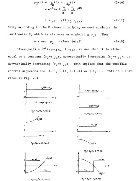
"l/a + ea t (7T2-1Tl/a) (2-17) Next, according to the Minimum Principle, we must minimize the Hamiltonian H, which is the same as minimizing P2U. Thus
u = -sgn p2 (since |u|^l) (2-18)
Since p 2 (t) = eat + ^l/a’ we see that it is either
equal to a constant (Tr2=Trl/a'> ’ mon°tonically increasing (1T2>7Tl/a^> or mon°tonically decreasing ^ 2 <v \fa) * This implies that the possible
control sequences are {— 1}, {+1}, {-1,4-1} or {4-1,-1}. This is illust rated in Fig. 2-3.
1
--0
p,(t)=Va
u(t)=-sgn R^t)= ■
-1
572 = 77i/a' 77i/a>0
u(t) = - sgnp,(t) = +i
Pa(t)=Va
7T2=7ij/a, 77;/a <0
Uw-1
TTj > 77,/a, 7T,/a>0
pjt)
U-+1
u = - 1
^> 7 ^ / 0 , 7T1/ a < 0
1 2
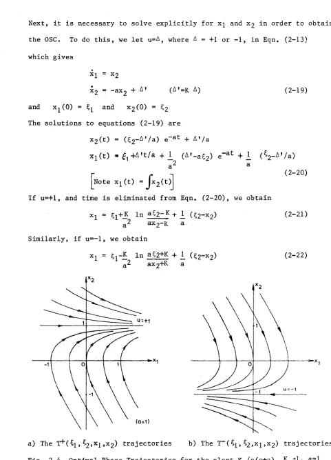
Next, it is necessary to solve explicitly for x^ and X2 in order to obtain the OSC. To do this, we let u=A, where A = +1 or -1, in Eqn. (2-13)
which gives
*1 = x 2
X2 = -ax2 + A 1 (A'=R 4) (2-19)
and Xj^(O) = and ^ ( O ) = %2 The solutions to equations (2-19) are
x 2(fc) = (?2-A,/a) e-at + A»/a
X l (t) » I ^ A ' t / a + 1_ (A'-aC2) e“at + I (^-A'/a)
a2 a
r c (2-20)
Note x^(t) = Ix2(t)
If u=+l, and time is eliminated from Eqn. (2-20), we obtain
x 1 = ?i+Jl a ?2~^ (C2-x 2^ a - ax2-R a
Similarly, if u=-l, we obtain
x = £ _K in ag2+K + (£2“x 2)
~2 axo+K a
(2-2 1)
(
2-
2 2)
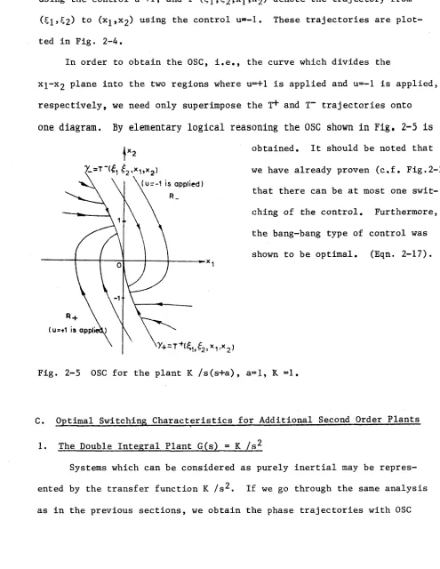
a) The T+ ( Cj , ?2>x l>x 2^ trajectories b) The T ~ ( , ?2»x l>x 2) trajectories Fig. 2-4 Optimal Phase Trajectories for the plant K /s(s+a), K -1, a=l
13
In order to make the definition of the phase trajectories more systematic,
we let ,?2>x1»x2^ denote the trajectory from (5i,£2) to (x l>x 2^ using the control u=+l, and T~(£i, £2»x l>x 2^ denote the trajectory from
(5l>£2) to (x l>x 2^ usin8 the control u=-l. These trajectories are plot ted in Fig. 2-4.
In order to obtain the OSC, i.e., the curve which divides the
xj-X2 plane into the two regions where u==+l is applied and u=-l is applied,
respectively, we need only superimpose the T"*" and T“ trajectories onto
one diagram. By elementary logical reasoning the OSC shown in Fig. 2-5 is
lx„ obtained. It should be noted that
we have already proven (c.f. Fig.2-3) that there can be at most one swit ching of the control. Furthermore,
the bang-bang type of control was shown to be optimal. (Eqn. 2-17).
(ur-1 is applied
Fig. 2-5 OSC for the plant K /s(s+a)
C. Optimal Switching Characteristics for Additional Second Order Plants
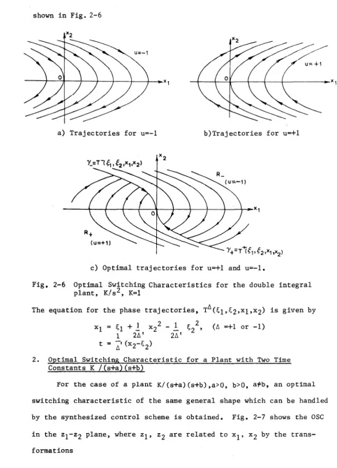
1. The Double Integral Plant G(s) = K /s^
Systems which can be considered as purely inertial may be repres ented by the transfer function K /s^. If we go through the same analysis
14
shown in Fig. 2-6
U = - 1
a) Trajectories for u=-l b)Trajectories for u=+l
?+=T (^v^2>xuX2) c) Optimal trajectories for u=+l and u=-l.
Fig, 2-6 Optimal Switching Characteristics for the double integral plant, K/s^, K=1
The equation for the phase trajectories, T ^ ( ^ , ^ 2 > x l5x 2) given by
X 1 = + 1 x 22 “ 1 ?92, =+1 or -1^ 1 2 A ' 2 A '
11 = a' (x2~^2)
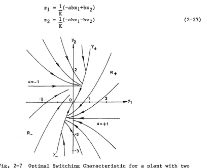
2. Optimal Switching; Characteristic for a Plant with Two Time Constants K /(s+a)(s+b)
For the case of a plant K/(s+a) (s+b) ,a>0, b>0, a.f=b, an optimal switching characteristic of the same general shape which can be handled by the synthesized control scheme is obtained. Fig. 2-7 shows the OSC
in the z^-Z2 plane, where z^, Z2 are related to X p X2 by the trans formations
1 5
zj = J^(-abx^+bx2) K
Z£ = J_(-abx^—b x 2) K
( 2 - 2 3 )
U = + 1
R_
Fig. 2-7 Optimal Switching Characteristic for a plant with two time constants, K / (s+a)(s+b).
This transformation is used to simplify computation of the phase traj
ectories by uncoupling the original state variables x-^ and X2«
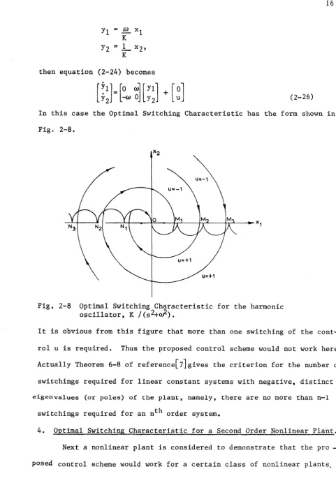
3. Optimal Switching Characteristic for the Harmonic Oscillator. K / (s^+o£)
This example is given to show that the proposed control scheme will not work for all second order plants representable in the phase plane.
An oscillator may be represented by the equation.
• « O
x + <u x = K u , (assume |u|^l, K >0)
whose transfer function is G(s) = K
(s24 W 2 )
If we let x^=x and x2 =x, and use the transformations
(2-24)
1 6
?1 = X 1 K
72 = i - x 2»
K
then equation (2-24) becomes
[ V 0 0) yi'
+ "o *
CM -co 0
.y2. u
In this case the Optimal Switching Characteristic has the form shown in Fig. 2-8.
U = -1
u=
U=41
U=41
Fig. 2-8 Optimal Switching Characteristic for the harmonic oscillator, K /(s^+ft^).
It is obvious from this figure that more than one switching of the cont
rol u is required. Thus the proposed control scheme would not work here. Actually Theorem 6-8 of referencejL]gives the criterion for the number of
switchings required for linear constant systems with negative, distinct
e i g e n v a l u e s (or poles) of the plant, namely, there are no more than n-1
f - " h
switchings required for an n order system.
4. Optimal Switching Characteristic for a Second Order Nonlinear Plant. Next a nonlinear plant is considered to demonstrate that the pro - posed control scheme would work for a certain class of nonlinear plants.
17
Consider the system (see section 7-11, [7]).
y + y|y| = u, |u|^i (2-27)
[Actually a more general form of (2-27) is
y + f(y) = K u, |u|$l, (2-28)
with certain c o n d i t i o n s on f(y), is given in reference 7 which would give
an OSC of a form to which the proposed control scheme could be applied] . The OSC and typical phase trajectories for the plant (2-27) are shown in
Fig. 2-9.
u=-f 1
u= -1
Fig. 2-9 The Optimal Switching Characteristic and phase trajectories for the plant y + y|y| = u, ]u|$l.
D. Analysis of Control Relay Dead-Time
Due to the physical properties of the components used for switch ing the control voltage to the armature of the motor, a finite length of time is required to switch the control from +1 to -1, and from -1
to +1. T y p i c a l r e l a y s w i t c h i n g c h a r a c t e r i s t i c s ar e s h o w n in Fig. 2— 10.
Details of the relays are given in section IV-C-2.
In order to be precise in the discussion of this section, the fol
lowing notation is used:
18
Fig. 2-10 Typical Control Relay Switching Characteristics,
t+,0
is the actual time that the relays switch from +1 to 0,
t-»° is the actual time that the relays switch from -1 to 0, t°»- is the actual time that the relays switch from 0 to -1, t°,+ is the actual time that the relays switch from 0 to +1,
+«
= t0 ’“ - t+ ’° (2-29a)
p “ »+ _ -,o + 6h - t - *C
■ » +
(2-29b)
-x.
switch to u=0
c o m m a nd u=+l
\due to
1
/
Fig. 2-11 Effect of 6^ and 6^ on the Phase Trajectories
1 9
It can be readily seen that 6^ and <$d represent a kind of "hysteresis-time" and "dead-time", respectively. The effect of
and 6^ on the phase trajectories will be typically as shown in Fig. 2-11. In the figure (Si m»5o") is the state of the system at t„+ , (£* F*)
i i. 1 2
is the state of the system at t *°, and is the state of the
system at t° ’+ .
In order to illustrate the method of analysis for the effect of the "hysteresis-time", 6^, and the "dead-time", 6^, the two plants K/s^ and K/s(s+a) shall be considered only. A similar analysis would
be used for other plants.
1. Effect of 6^ and for the Plant K/s^
2
For the plant K/s , we have
* 1 = x 2
x 2 = A' (A'=KA, A=±l) (2-30)
The solution to (2-30) is x 2 = ^2 ^
x l = ?i + S2t + %A't2 . (2-31)
Using the notation specified above, at t+,° or at t ,0 we have e2’ - s2" + a-«h
5 l ' - ? l " + 526h + ’ (2_32)
and at t ° ’ or at t° ,+, we have (i.e., A==0 in (2-30)),
g2 = ?2
= h ' + K2 & d (2"33)
r I e I
Eliminating ^ and 2 from (2-32) and (2-33) gives
?1 - Cj +
qsh
+ >SA'62 + {26d . (2-34)2 0
compares to the value of £i which is stored in the memory of the computer. We see that (2-35) is of the form
h = Si" + + c 2KA (2-36)
The constants c-^ and C2 (defined by 2-35) are known, and depend only on the physical properties of the relays which are used. If the constant
K were known (it depends on the plant, whose parameters are assumed to
be unknown) eqn.(2-36) could be inputted to the computer program and the effects of 6d and 6^ would be accounted for in the switching logic. However, if c^ and c 2K are assumed unknown they could be estimated from (2-33), (2-34), and (2-35) by observing the state (xj,x2 ) during the first control period as shown below.
I
in itia l s ta t eFig. 2-12 Effect of 6h and 6d during first control period
T h e n f r o m (2-34),
K 6h «ai = (52-52")/A (A = ±1) (2-37)
and from (2-33)
<5d - a 2 = (Ci-£1 ,)/£2t (2-38)
and from (2-35)
6h ~ a 3 “ (Si- S2'{l+a2 } “ Aa1a2)/(SI2 + Aa1/2). (2-39)
21
Then C1 = a 3 + a 2
c2K = + a 2) , (2-40)
and (2-36) could be used to account for 6^ and 6^. Logic must be provided in the computer program to account for the case £ ’ = 0
and/or (£2" + Ao^/2) = 0. Actually (£-^',£2"), (C1'»C2 ,)» and could be determined during the first control period by physically
sensing whether u is positive, negative, or zero, and observing the states (xj,x2) at these times. Practical considerations and topics for
further study in regards to 6^ and 6^ are discussed in section VII. 2. Effect of 6^ and 6^ for the Plant K/s(s+a)
For the plant K/s(s+a), we have
xi = x2
x2 =-ax2 + A' (A* = KA) (2-41)
and from section 11-B, the optimum phase trajectories are specified by
x2 = (£2-A'/a)e-at + A'/a
x, = + A ' t/a + — (A'-a£2)e~at + i ( S2- A ’/a) (2-42)
1 1 a2 a
Using the notation specified above, at t+ »° or at t- ’0 we have
S2 ' = (52M- A V a ) e - a<5h + A ’/a
Sj' = +A'<5h/a + — (A’-a5 2")e-a6h + I ( ?2"_ A »/a ) (2-43)
a2 a
and at t°* or at t ° ,+, we have (i.e., A=0 in Eqn. 2-41) S2 = e-a «d S2 '
Si = — (l-e_a6d) + 5 - (2-44)
a
ThUS 5 = e-a (6h+<5d)r " + A i (1_ e-a{5h+<sd})
2 a
5 , { » + i(l - e-a{Sh+id 2" + — <«„+ia-a6,,{e-aii,-l))
*■ 3, 3 . c l
2 2
used to compensate for 6^ and 6^ by looking at the present state 5"),
computing the projected state and then comparing (5i>?2) with that stored in the computers memory.
If these parameters are not known then we might proceed as in
the previous section and use equations (2-43) to (2-45) to determine
the unknown coefficients in (2-45) in terms of the observed states (£",£")>
(£{,£2) and (£i>?2) during the first control period.
23
III. DIGITAL CONTROL COMPUTER MODIFICATIONS
Although a large part of the digital control computer had been constructed, considerable changes had to be made to both the design and wiring. Because these modifications and additions were quite extensive,
the author felt a section should be devoted to show these changes. For the future, a complete set of logic diagrams will be available.
As closely as possible, the order of the diagrams and explanations will be the same as those used by the original designer [8], In this
section, the title and page number in brackets on each figure, are the same as those used in Ref. 8. Therefore, if the original design is used to
augment the explanations, the reader should find no difficulty in following this section.
Multiplication Order
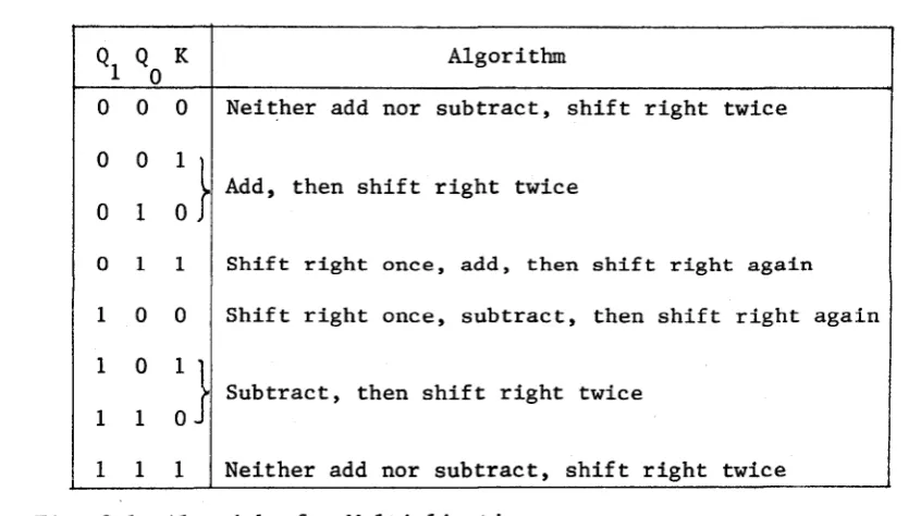
The computer uses a serial repeated addition and subtraction method. The algorithm for multiplication in the signed 2 ’s complement form is shown in F ig. 3-1.
Q 0
K Algorithm
0 0 0 Neither add nor subtract, shift right twice
0 0
U Add, then shift right twice
0 1 o J
0 1 i Shift r ight once, add, t h e n shift right a g a i n
1 0 0 Shift right once, subtract, then shift right again
1 0
‘ 1 Subtract, then shift right twice 1 1 o J
2 4
Eight phases are required to carry out the multiplication order. The operation is as follows: during the first phase, the contents of the
Accumulator (A-Register) are shifted into the Q-Register. For the fol lowing six phases, three digits (the two least significant digits of the Q-Register and a bit held in the K-flip-flop) are examined and the
contents of the appropriate registers are operated upon according to the algorithm in Fig. 3-1. In the eighth phase, the contents of the Q-Register are shifted into the A-Register.
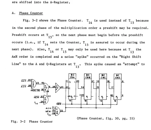
A. Phase Counter
Fig. 3-2 shows the Phase Counter. T is used instead of T because
14 15
in the second phase of the multiplication order a preshift may be required. Preshift occurs at T , so the next phase must begin before the preshift occurs (i.e., if T , sets the Counter, T is assured to occur during the
14 ’ 15
next phase). Also, T , or T may only be used here because at T the
14 15 13
AxH order is completed and a noise "spike" occurred on the "Right Shift Line" to the A and Q-Registers at T . This spike caused an "attempt" to
BC C9A
BC C 9B
BC C9C
BC C9D
AxH 20 27 10
123 19,
A - f H 3 4
10 M O D .O IJ —
32D 8D
22 N E W
N E W
A f H — NEW -25.
r.-sa
(Phase Counter, fig. 30, pg. 55) Fig. 3-2 Phase Counter
right-shift the A and Q-Registers after Q-*-A occurred in the eighth phase. During the eighth phase, right-shifting pulses are inhibited by P P P P
25
at gate C12A of the "Right Shift Accumulator" shown in Fig. 3-9. At the same time, P P P P at gate C13C, in conjunction with T at C8B determine
0 1 2 3 13
NEW. NEW in turn, resets the Phase Counter. The change had to be made in order that during the eighth phase no right-shift information occurred
until after the AxH order had been completed when it no longermattered. Fig. 3-3 shows the waveforms produced by the Phase Counter during an
AxH order.
'13
A X H
P0
multiply order '13
1
1)4 1 )4 1)4 t 14 T14 t 14 Fa t 13
. T "
'13
P. P. P„
0 1 2
T1'3 T14
p2 - | A ^ r
T1J — jQ + A
P P
Fig. 3-3 Multiplication Order Waveforms
Initially the Phase Counter is set at 0000 and counts up to 0111 (7). Then NEW resets it to 0000 again. The original counter was set to count six phases (i.e., 1 0 H 5 , 10*15, ...). Gate C4B has been left
because it does not affect the AxH order. However, in the future when the divider is made operational, it will have to be changed or removed entirely.
B . M u l t i p l i c a t i o n U n i t
Fig. 3-4 shows a block diagram of the Multiplication Unit. Gate D17A eliminates ADD or SUBT signal from being generated during the eighth
2 6
A x H 14i
N E W 15 18 D \i7V
-16D C J
T15
Q ^ 2 6 1"~'s'\29 Q o 27 16 ID \
K 26 F J
PRESHIFT
P R E S H I F T
F r o m Div. Unit
A x H
6 31
8 D
N E W
F r o m Div Unit 10
3 2 ET
112 29
AxH
N E W
A D D
suit
Go
V RIGHT SHIFT
Q - R E G
FA C 2 3 B 3 3
3 4 , )
22 A 21
o
2 0 31
(Multiplication Unit, fi g .29,pg.54)
C R 1 3 B has been cut
Fig. 3-4 Multiplication Unit
by a change in , Q q or K at gates D18H or D17E respectively during any phase of the AxH order.
The multiplication operation can best be explained by an example. Two examples are shown so that the handling of a negative number can also be
illustrated.
In signed 2 rs complement
7 = 0,00000000111 (initially in A-Register) 3 = 0,00000000011 (initially in an H-Register)
27
Phase no. QiQoK
Operation Contents of A-Register
4 1A10A9A8A7A6A5A4A3A2A 1A0
Contents of Q-Register
Q llQ lo Q 9 ^ 8 ^ 7 ^ 6 ^ 5 ^ 4 ^ 3 ^ 2 ^ 1 ^ 0 K
init 0 0 0 0 0 0 0 0 0 1 1 1 0 0 0 0 0 0 0 0 0 0 0 0 0
1 A+Q 0 0 0 0 0 0 0 0 0 0 0 0 0 0 0 0 0 0 0 0 0 1 1 1 0
2 l 1 0 Subt(A-H) 1 1 1 1 1 1 1 1 1 1 0 1 0 0 0 0 0 0 0 0 0 1 1 1 0
shift rt 2 1 1 1 1 1 1 1 1 1 1 1 1 0 1 0 0 0 0 0 0 0 0 0 1 1
3 0 1 1 shift rt 1 1 1 1 1 1 1 1 1 1 1 1 1 1 0 1 0 0 0 0 0 0 0 0 0 1
Add (A+H) 0 0 0 0 0 0 0 0 0 0 1 0 1 0 1 0 0 0 0 0 0 0 0 0 1
shift rt 1 0 0 0 0 0 0 0 0 0 0 0 1 0 1 0 1 0 0 0 0 0 0 0 0 0 4 0 0 0 shift rt 2 0 0 0 0 0 0 0 0 0 0 0 0 0 1 0 1 0 1 0 0 0 0 0 0 0
5 0 0 0 shift rt 2 0 0 0 0 0 0 0 0 0 0 0 0 0 0 0 1 0 1 0 1 0 0 0 0 0 6 D 0 0 shift rt 2 0 0 0 0 0 0 0 0 0 0 0 0 0 0 0 0 0 1 0 1 0 1 0 0 0
7 0 0 0 shift rt 2 0 0 0 0 0 0 0 0 0 0 0 0 0 0 0 0 0 0 0 1 0 1 0 1 0
8 O+A 0 0 0 0 0 0 0 1 0 1 0 1 0 0 0 0 0 0 0 0 0 0 0 0 0
7x3 = 16+ 4 + 1 = 21
Fig.3-5a Multiplication of 7x3
-8 = 1,11111111000 (initially in A-Register) In signed 2's complement
3 = 0,00000000011 (initially in an H-Register)
Phase no.
QiQoK
Operation Contents of A-Register
H 1A 10A 9A 8A 7A 6A 5A 4A 3A 2A 1A 0
Contents of Q-Register ^11^10^9^8^7^6^5^4^3^2^1^0 K
init 1 1 1 1 1 1 1 1 1 0 0 0 0 0 0 0 0 0 0 0 0 0 0 0 0
1 AM) 0 0 0 0 0 0 0 0 0 0 0 0 1 1 1 1 1 1 1 1 1 Q n n n
2 0 0 0 shift rt 2 0 0 0 0 0 0 0 0 0 0 0 0 0 0 1 1 1 1 1 1 1 1 1 0 0 3 1 0 0 shift rt 1 0 0 0 0 0 0 0 0 0 0 0 0 0 0 0 1 1 1 1 1 1 l l l 0 Subt (A-H) 1 1 1 1 1 1 1 1 1 1 0 1 0 0 0 1 1 1 1 1 1 l l l 0 shift rt 1 1 1 1 1 1 1 1 1 1 1 1 0 1 0 0 0 1 1 1 1 1 l l l 1 4 1 1 1 shift rt 2 1 1 1 1 1 1 1 1 1 1 1 1 1 0 1 0 0 0 1 1 1 l l l 1 5 1 1 1 shift rt 2 1 1 1 1 1 1 1 1 1 1 1 1 1 1 1 0 1 0 0 0 1 l l l 1 6 1 1 1 shift rt 2 1 1 1 1 1 1 1 1 1 1 1 1 1 1 1 1 1 0 1 0 0 0 1 1 1 7 1 1 1 shift rt 2 1 1 1 1 1 1 1 1 1 1 1 1 1 1 1 1 1 1 1 0 1 0 0 0 0 8 Q-*A 1 1 1 1 1 1 1 0 1 0 0 0 0 0 0 0 0 0 0 0 0 0 0 0 0
1 1 1 1 1 1 1 0 1 0 0 0 = -■24 (signed 2's compl.)
Fig.3-5b Multiplication of -8x3
C . Delay Line Memory
Fig. 3-6 shows a block diagram of the Delay Line Memory. Information is continuously being circulated. Input/output to/from the delay line memory occurs only during COMPARE or MOD.OP. operations.
2 8
S-order signal at A4A and COMPARE signal at A5A occurred. Hence, stored information would not circulate. At the same time, information at ENTER
would be allowed to enter when it is not desired to do so.
29
Delay
C O MPARE — 30
ENTER — W —
Delay Line Pac 30
Clock T -- (Delay Line Store-s, fig,17?pg.36) Fig. 3-6 Delay Line Memory
D. Gating of Accumulator
Fig. 3-7 shows a block diagram of the Accumulator Gating. The changes
here are quite extensive. In the original design, gates C10C, C11G, and C12C were used to restore the sign bit in the Accumulator after the first phase of the AxH order. There is no point in doing this. A review of the multiplication operation will clearly show that this recirculation is not required. Gates D16D, D15E, and D17G were used in the first phase of the
AxH order to recirculate the contents of the Accumulator. Since the multi
plication operation does not require this recirculation, the gates have been removed.
The COMPL. signal at gate A2G is used during the |AI-*A order when 2's complementing a negative number is required. Gate C15D is used to restore the sign bit during the AxH order. It is restored in the eighth phase (i.e., Q+A). This is necessary because in left shifting there is no con nection between A ^q and A ^ (i.e., no information can be left-shifted into
2 9
TO SC '
.23 A- REG. S U B T
A + H A + S
A - S
C O M P L
3 0 R IG H T
SH.---7 D 15Q.
7D T O SC
6 A - R E G . 10
J m O & . o p — !2
7 E N T E R —
T O R C A - R E G . A - H
S-*A
Rt^a T O RC
A-REG.
A->S A^iH
______ 150 J U M P t A i O ) --- —
15D
A * 1 1 5D IaI— a - hn\16|
10
C O M P L —
35 2 5 33
280 2 5 i3 3
2 8
2 6 2 8
2 7 2 8 2 9
15 3 2
L E F T SH. 12
(Gating of Accumulator, fig,19.pg.39) Fig. 3-7 Gating of Accumulator
the sign bit location ( A ^ ) of the Accumulator).
E. Accumulator
Fig. 3-8 shows a block diagram of the Accumulator (A-Register), Q-Register and the input from the Shaft Position Encoder. The circuit for resetting the Q-Register and K-flip-flop (C14C and D15H) is necessary because if there were any digits left in the Q-Register from the previous multiply order or from initial turn-on of the system, during the first phase (A*Q) the unwanted digits will move into positions Q^, Qq , or K and
set ADD or SUBT signal which gates the ENTER to the Accumulator. Therefore,
30
UF
C 1 7 A
UF C17B
UF
C18A C180UF C19AUF C19BUF C20AUF
U F
C2O0
25 16 25
24 17 24 24
26
30S C 30 30
23 23 23
10
R I G H T S H I F T 22
L u
20 20 2 0
RQ
32 32 32
LEFT SHIFT 23 10 A-REGISTER 23 15 22 UF D22A UF D24B UF
D23A D23BUF UF
D24A (25
F F
02 7D 25
24 14 26 26 15 13 30 23 18 23 23 20
.
17 32D 35 16 13^ 17 14RIGHT SHIFT LI NE
LEFT SHIFT LINE
Q-REGISTER
31
FA C23D
INPUT. 12 INPUT
,+12 V 11 INPUT
16 19 220 From shaft Position encode 14 UF C22B UF C21B UF C22A U F C21A Output 25 .16 NC (Is -12V Cannon connector K02-16-10PN 22 27 29
+ 12V
25
25
|33
25 31 23 25
10 K Interrogate pulses
-6 v FA
B1C
2 5 2525 CLEAR INPUT
10 TT. UF 019 B UF D20B UF DI9 A UF D21B UF D20A UF D22B UF 0 21 A
18 23 23 23 1 0 31 20 20 20
Clears Q-Reg in 1st
*6 —
B- 28024
[28 [35
(Accumulator, fig. 18, pg. 38)
33
34
32
The signal marked Z, at the output of flip-flop D27D, allows in
formation to flow from the A-Register to the Q-Register between times and T^, during the AxH order, and is used to gate the ADD or SUBT signals. This is necessary because while the information is being shifted to the right in both registers, at times T 13» t15» or T 0 , the digits in Q p Q q , or K
may become such combinations as to generate an ADD or SUBT signal which
would enter information to the Accumulator from the Arithmetic Unit by the
ENTER path.
Because the Optical Shaft Position Encoder has serial output inform ation with most significant digit first, and, since the computer INPUT information is moved around least significant digit first, during the order, ten (Interrogate) left-shifting pulses serially move inf
ormation into the least significant position of the A-Register. Left- shifting pulses (T^-T]^) are already available, so, rather than generate
pulses ( T ^ - Tj q) , INPUT* signal opens gates C25E and C25B during only ten pulses.
Originally, the Accumulator could be cleared manually, only. However, during the INPUT order, only ten left-shifting pulses are used, so that, if the least significant digit (Aq) was present before the INPUT order was called, it would be shifted to the overflow position (A^q). Gate A25B is used to clear the ACCUMULATOR just prior to accepting information from the Shaft Position Encoder as well as for manual clearing. A25D acts as an
i n v e r t e r .
F . Right and Left Shifting the Accumulator
Fig. 3-9 shows a block diagram of the logic for providing right and left-shifting pulses. Here changes were considerable but the logic is easy to understand, therefore, only the less obvious changes will be
33
C \ RIGHT SH.— 34
80
\PA
X 32/ TO RIGHT SHIFT
16 > - 1 ^ — LINE OF A-REG.
% *
340
A-*-H -
£*-A-^HtCL -^2-
JUMP(A*Q) -24.
iahTa" ^
22 34D 26, 26 29D .COMPARE- 14 27
29 D
13 ) MOD. O R —
28
A t S
30 20
A - S TO RIGHT SHIFT
. LINE OF Q-ftEG.
28
26 30
B ^ 9 LEFT SH.— A D D
23
26 28
SUBT
,34 34
25
Ax H — ^
______ 28D 20
he TO LEFT SHIFT
LINE OF A-REG.
10 280 20 AxH PRESHIFT -25 _________ 34 280 28 32 20D 20 25
22 r 35 22
13-- 30
Ax H
23
24 >27 14
29
PRES HI F T -2^-
________ 32D 34 PA
TO LEFT SHI FT LINE OF O - REG. 132
30
200 12D
14
A X H —
32
(Right and Left Shift Accumulator figs.20 & 21,pgs. 40 & 41)
14
35 33
8D
34
Fig. 3-9 Right and Left-Shifting the Accumulator
described. Gate C14A provides a "1" at C15C, C11H, and C11G for the seven last phases of the AxH order. For the first phase (A->Q) it inhibits Tj^
to T 13 '
The signal marked X is required to prevent right shift pulses during
the eighth phase (i.e., Q+A) of the AxH order. Gate B3E has been used to replace C15G in the original design because three inputs were required.
34
required as Interrogate pulses for the Optical Shaft Position Encoder
(see "Accumulator" Fig, 3-8).
G. I-Registers
Fig. 3-10 shows a block diagram of the two Index Registers. In the original design, no provisions were made to either select the proper
register or circulate its contents during the modification operation (MOD.OP.). An added order, A-*-I is also shown. For the A-»-I order, the network shown was necessary to provide both positive and negative going
shift pulses at the I-Registers because the I-Register shift pulses are positive-going while the Accumulator (A-Register) uses negative-going pulses.
M O D OP
SR D2A SR D2B SR D2C SR D2D FA
D 4 A
F A D 4 B
M O D O P ^3.
ENTER — \23
24 29 33 19 25 10 23 28 33
29 34 _16 \34 SHIFT 26 22 Uo 33 k25
115 114 113 112 1I0
29
SHIFT I R<
\Z7
22
M O D OP
SR
D3A D3BSR
SR
D3C D3DSR
FA
D4C D4DFA
10] D M O D OP
24 29 33 25 10 15
16 ENTER
16 SHIFT
MR.
33 2 5 ; ,10
SHIFT IR2
20 22
27
SHIFT IR. SHIFT *IR, 20 30
29
32 [24D 23
31 25 SHIFT IR. 10 18 15D 8D
(I-Registers, fi g .24, p g .47) A-I
(T.-V J! H
Fig. 3-10 I-Registers
3 5
H. Inversion Gating
Fig. 3-11 shows a block diagram of the Inversion Gating. Changes here
are few. Several new orders have been added and the flip-flops required resetting in order that no order involving the memory was activated during
initial turn on of the computer.
START BUTTON V"
H—»A A—»H
A-»HACL
A + H —
A - H —
AXH_ _
IA^' A
H=*S 10 S-~A
11 A—
12 A-**S4CL
13 A + T
14 A - S
15 Spare
16 RIGHT SHIFT A
17 LEFT SHI FT A
16 JUMP (A <0)
19 JUMP (AjiO)
20 N—►!
---21 r+TTJT — ■—
22 I-N-»I
---23 A-*I
----24 TEST M O D
-25 Spare
26 INPUT
--27 OUTPUT-
26 Spare
29 U JUMP ■
30 Sa l t
31 Spare
START
A X H
f/
— A >1AI
33
RIGHT SHIFT A
LEFT SHIFT A
JUMP (A<0)
JUMP (A/O)
N-*I
-22. A-el
TEST M O D
INPUT
OUTPUT
B\16 U JUMP
I NCREASE
INITIALIZE IC
r-FF B5B
21. <
LI FF C6C J-22 22 FF C6B ii-A FF C7A 16 FF C7D 25 FF C6A 26 FF C7B (Inversion Gating,fig.26,pg.50) Fig. 3-11 Inversion Gating
I. Adder/Subtractor
Fig. 3-12 shows a block diagram of the Adder/Subtractor and its inputs. In the original design no provision was made to clear the CARRY flip-flop prior to an arithmetic order. Initial turn-on of the computer or a previous arithmetic order could leave it in either state.
S o r H o r N o r l 36
n -<8 w-<
< rt
<0 £
to2o 'ffl—u
CO in to cu 00 <NI bO •H O 4J O Ctf M ■U #n
CO
1-1 a) no !2 6 M O ■M O rt t-l 4J »jQ rt cn M ai T3 3 cs 1-^ I CO 60 •H to
37
during a modification order leading edge positive-going pulses are required
while H-Registers use trailing edge negative-going pulses. Gate B15F acts
as an OR gate, therefore, negative-going pulses or Positive" going pulses (T^-Tg) are available at the CARRY flip-flop.
Gates B3D, B3F, and flip-flop BIB are part of the complementing
order, A-*|a|. During this order, at time Tq, the sign bit of the Accumulator,
A-q, is sensed. If Aj^ is "0" (i.e., positive value), the contents of the Accumulator are merely recirculated (see Fig. 3-8). But, if A ^ is "1"
(i.e., negative number), the subtraction of the contents of the Accumulator from ZERO is performed, which is the same as taking the 2's complement of the number in the Accumulator.
J. Bit Counter and Timing Unit
Fig. 3-13 shows a block diagram of the Clock, Bit Counter, and Timing Unit. The maximum serial read-out rate for the Optical Shaft Position
Encoder is only 100 kHz. The Computer has a clock rate of 200 kHz. A simple means of producing INTERROGATE pulses at the lower rate was to reduce the Clock speed by half. Normally gate CIA is open and C1B closed by the INPUT signal: the output of ClB is at "1" so the pulses at clock
rate of 200 kHz are provided by power amplifier C24D.
Flip-flop B1A continuously divides the Clock rate by two. When the Shaft Position Encoder is interrogated during the INPUT order, gate CIA is closed and ClB is open to allow pulses at half the clock rate to be present at C24D. ClC resets BlA before the INPUT order but not during: this is important for pulse shaping.
In generating INPUT* signal (see Fig. 3-8) T ^ was required. Since
Tg was not necessary in the computer, gates D12D and D12H were used to save
M
C
38
oo»u \ 7 a o > x
R e p ro d u c e d w ith p e rm is s io n o f th e c o p yrig h t o w n e r. F u rth e r re p ro d u ctio n p ro h ib ite d w ith o u t p e rm is sio n .
F
i
g
,
3
-1
3
B
i
t
C
o
u
n
t
e
r
a
n
d
T
i
m
i
n
g
U
n
i
3 9
Power amplifier D14A has been used for signal which is required
in the LOCATION ENCODER (see Fig. 3-17). At the time it was the only power amplifier available. The power requirements for T ^ are low, so, DlA was
used.
The TEST. MOD. signal was necessary at gates D15C and D15D to inhibit (T^-Tg) during the TEST MODIFIER operation (i.e., this order is two word lengths in duration).
Not shown in Fig. 3-13, are two gates in cascade between B3G and ClB.
Gates D5H and C10C, were required to provide enough "delay" in turning off
the INPUT signal at time T^g, to prevent a "spike" when the pulses, provided by the divider BlA, are inhibited and taken from the clock (at this time, the two signals were at the same levels). This "spike" was of sufficient
duration to add an extra "count" in the BIT COUNTER.
K. (Control) N-Register
Fig. 3-14 shows a block diagram of the Control Register. The original
design shows that the contents of this register is recirculated for each of the following orders: I+N-KH, I-N-KL, and N*I. There is no purpose in
ENTER
29
,27 29 19 25 24
25
3 16 16
— Ha 29
25
25
8D N -*■!
14 25
MOD. OP.—
INCREASE
--(Control Register, Fig.34,pg,60)
SHIFT
SR
A23A A24BSR
SR A2 3D SR
A23B A23CSR A24 SR A
40
this since the number N is obtained from the "LOCATION ENCODER", shown
in Fig. 3-17. N is inserted into the Control Register at time (i.e., one clock pulse after the beginning £at T j ^ of any of the above orders). The other changes are minor.
L. Compare Unit
The Compare Unit is shown in Fig. 3-15. This unit compares the numbers in the WORD COUNTER and in the (Control) N-REGISTER. If the numbers are
20
22
° 17 127
20 29
F F B 5 C 23
20 25
24
is- C O M P A R E 25
20
30 20
MOD OP U R
— C O M P A R E 20
18
20
134
20
L33
25
10
19
,16 30)
[23 26
W .
22
(Compare Unit, fig. 36, pg. 62)
22 14
Fig. 3-15 Compare Unit
41
the same, the COMPARE flip-flop is set. The next word to come out of the DELAY LINE (memory) is then the required word.
This unit is used during the modification (MOD. OP.) operations as well as during the S-orders. During an address modification operation, at
which time the numbers in the WORD COUNTER and CONTROL REGISTER are the
same, the COMPARE Signal is produced at time Tq, at which time information may be inserted into, or retrieved from, the circulating memory at the
location in memory given by the number in the Control Register.
M. Word Counter
Fig. 3-16 shows the WORD COUNTER. The WORD COUNTER assigns a "count"
or number to each word in the memory. Only 60 words can be stored in the delay line memory, therefore, this counter advances from 61 to 63.
INPUT
B C A 1 4 A
B C A 1 4 B
B C A 1 9 A
B C A 1 9 B
B C A 1 9 C
BC
A 1 9 D
2 0 * 0 27 *1 2 0 CM 27 16 *4
3 4 22 3 4 15 17
02 5 J * b 33 W 1 2 5 W 2 33 * 3 12
W0 W 1 w 2 W 3 W4 W 5
(Word Counter, Fig. 35, pg. 61)
Fig. 3-16 Word Counter
4 2
during the INPUT order, to "keep up" with the information flow in the
delay line. Tq was chosen because it is the only signal which was avail
able without adding an inverter (see Fig. 3-13).
N. Location Encoder
Fig. 3-17 shows a block diagram of the Location Encoder. The COMPARE signal resets flip-flop D27A which in turn gates DIB to allow T ^ to insert
P N
F F D 2 7 A M O 0.0 P. -Afi
L 5 9
26
L55 26
33 25i 133 10
.24 23
L47 26
L 6 0
L 5 8 L 57 L 56 27 20_ L31 34 L 54 L 5 3
L 5 2 131
25 L 50
L 4 9 L 4 6 L2 4 L23 L22 L21 L20 L19 L18 L17 L16 L15 L14 L1 3 L1 2 L11 L 1 0
127 L 4 6
L 4 5 L44 L4 3 L4 2 L41 L 4 0 L39 L 3 8 L 37 L. 36 L 3 5 L34 L 3 3 L 3 2
10
2 9 1Z
30 30 23 12 3 L7 L o L 5 1 4 L 3 26
L 3 0
L 2 9
L 26 L 27 L 26
L 25 „, Typical diodein matrix
(Location Encoder, fig. 40, pg. 68) L O
Fig. 3-17 Location Encoder
43
the number N from the Location Encoder into the Control Register
(see Fig. 3-14). The modifications were necessary because according to the original design there would be an attempt to insert a number into the Control Register at every T ^ .
For S-orders, if MOD.OP. is true, the order is prohibited until modification is completed.
0. Increase I.C. Gating
The block diagram for the "Increase Instruction Counter Gating" is shown in Fig. 3-19. This works on the prohibition principle. That is,
inputs to D 1 4 C
the Instruction Counter is advanced at every T-^g by the INCREASE I.C, signal, unless this signal is prohibited. Prohibition occurs if:
(1.) an S-order is incomplete
(2.) a multiplication (AxH) order is incomplete (3.) a JUMP signal has been produced
(4.) a TEST signal has been produced
(5.) the START flip-flop has been reset.
Flip-flop D26C inhibits the instruction counter from advancing on the first count, during an S-order. Fig. 3-18 showing a time diagram, illus trates how the Instruction Counter is inhibited for two orders, mentioned in the list above. The second order (JUMP) follows the first (TEST MOD.) by two word lengths in this example only.
^ T1 T13 tp ] « T1? T1 3 T1 t1 3to t13
(i n c r e a s e 1 U |f U I F 1
IT-t e s IT-t M O D | [_
JU M P
(output) INCREASE LC.
J l
44
The NEW instruction flip-flop is required in the multiplication (and
division) order. It is used to gate the operation of the first phase
(see Fig. 3-2).
A + S
PA 24 D 25
25 A - ^ S & C L —
23
I N C R E A S E
20|P/\ 26/30 <0 24
13
---.30 19 1a 25 I N C R E A S E IC
28D 20
C O M P A R E —
34
J U M P
35 T E S T
33 FF
C 5 A 35
25 28
34 N E W
2 5 N E W 30
\2 3
26 33
N E W A-r H Stop/Start Flip-Flop Inhibit Restart Flip- Flop FF D 2 6 C
FF
D 2 6 A
FF
D 2 6 0 S T A R T
20 26
25 25
15D 22 H A L T
-25 29
S T O P
(Increase I.C. Gating fi g » 42, pg. 70) Fig. 3-19 Increase Instruction Counter Gating
P . J u m p / T e s t L o g i c an d I n s t r u c t i o n C o u n t e r
Fig. 3-20 shows a block diagram of the Jump/Test Logic and Instruction Counter. Most of the changes are minor. The important change is that INCREASE I.C. instead of INCREASE is used to advance the Counter. The
modification (MOD. OP.) operation requires two word lengths. The first phase is a compare phase and in the second the actual order is executed.
R e p ro d u c e d w ith permission of th e c o py ri g h t o w n e r. F ur th e r rep ro duc tio n pr o h ib it e d w it h o ut p e rm is s io n . JUMP(A/0) Moaop JUMP(A<0)
j u m p/t e s t
U JUMP MOD. OP.
BC A1tA JUMP
A M D
-WCRCASE ia
JUMP MOD. OP.
j u m p/t e s t 2fi
Manual Counter
IIjj^TEST MOD. 159
13 '
? \12 SOD A IO A A1OC
er-w
15DfT\TEST M O D —
A10D
(Jump/Test Logic, fig. 37, pg. 63) (Instruction Counter, fig. 38, pg. 65)
46
IV. DESCRIPTION OF HARDWARE
A. General Description
The actual system to be controlled was a 1/15 hp-dc motor con nected through a set of gears to an optical shaft position encoder.^
A differential gear was used to set the initial position manually. Con nected directly to the shaft of the motor was a 35 lb.-4 inch radius, steel disc. This large load was used in order that the overall system could be regarded as approximately purely inertial and in order that
the system moved slowly enough for the digital controller. Fig. 4-1
shows a block diagram of the set-up. Referring to Fig. 4-1, the vert
ical input of an oscilloscope was connected at a and the horizontal input was connected at b.
1/I5hp motor 115vdc 0 8 a mp 1725rpm
steel
9l— 1 :32
= differential gear
92 =1:2
93=112
3 M model 203524 shaft position
encoder
Ijn© set manually
Fig. 4-1 Block diagram of the hardware set-up
Since their effects are small in comparison to those of the load, an idealized version of the differential gear (with no appreciable
t see reference 11.