University of Windsor University of Windsor
Scholarship at UWindsor
Scholarship at UWindsor
Electronic Theses and Dissertations Theses, Dissertations, and Major Papers
10-10-2018
An Improved Public Unclonable Function Design for Xilinx FPGAs
An Improved Public Unclonable Function Design for Xilinx FPGAs
for Hardware Security Applications
for Hardware Security Applications
Siva Prashanth Balasubramanian University of Windsor
Follow this and additional works at: https://scholar.uwindsor.ca/etd Part of the Electrical and Computer Engineering Commons
Recommended Citation Recommended Citation
Balasubramanian, Siva Prashanth, "An Improved Public Unclonable Function Design for Xilinx FPGAs for Hardware Security Applications" (2018). Electronic Theses and Dissertations. 7595.
https://scholar.uwindsor.ca/etd/7595
This online database contains the full-text of PhD dissertations and Masters’ theses of University of Windsor students from 1954 forward. These documents are made available for personal study and research purposes only, in accordance with the Canadian Copyright Act and the Creative Commons license—CC BY-NC-ND (Attribution, Non-Commercial, No Derivative Works). Under this license, works must always be attributed to the copyright holder (original author), cannot be used for any commercial purposes, and may not be altered. Any other use would require the permission of the copyright holder. Students may inquire about withdrawing their dissertation and/or thesis from this database. For additional inquiries, please contact the repository administrator via email
An Improved Public Unclonable Function Design for Xilinx FPGAs for Hardware Security Applications
By
Siva Prashanth B
A Thesis
Submitted to the Faculty of Graduate Studies
through the Department of Electrical and Computer Engineering in Partial Fulfillment of the Requirements for
the Degree of Master of Applied Science at the University of Windsor
Windsor, Ontario, Canada
2018
An Improved Public Unclonable Function Design for Xilinx FPGAs for Hardware Security Applications
by
Siva Prashanth B
APPROVED BY:
______________________________________________ N. Kar
Department of Electrical and Computer Engineering
______________________________________________ S. Das
Department of Civil Engineering
______________________________________________ M. Khalid, Advisor
Department of Electrical and Computer Engineering
______________________________________________ M. Mirhasanni, Co-Advisor
Department of Electrical and Computer Engineering
iii
DECLARATION OF ORIGINALITY
I hereby certify that I am the sole author of this thesis and that no part of this thesis has
been published or submitted for publication.
I certify that, to the best of my knowledge, my thesis does not infringe upon anyone’s
copyright nor violate any proprietary rights and that any ideas, techniques, quotations, or any
other material from the work of other people included in my thesis, published or otherwise, are
fully acknowledged in accordance with the standard referencing practices. Furthermore, to the
extent that I have included copyrighted material that surpasses the bounds of fair dealing within
the meaning of the Canada Copyright Act, I certify that I have obtained a written permission
from the copyright owner(s) to include such material(s) in my thesis and have included copies of
such copyright clearances to my appendix.
I declare that this is a true copy of my thesis, including any final revisions, as approved
by my thesis committee and the Graduate Studies office, and that this thesis has not been
iv
ABSTRACT
In the modern era we are moving towards completely connecting many useful electronic devices
to each other through internet. There is a great need for secure electronic devices and systems. A
lot of money is being invested in protecting the electronic devices and systems from hacking and
other forms of malicious attacks. Physical Unclonable Function (PUF) is a low-cost hardware
scheme that provides affordable security for electronic devices and systems.
This thesis proposes an improved PUF design for Xilinx FPGAs and evaluates and compares its
performance and reliability compared to existing PUF designs. Furthermore, the utility of the
proposed PUF was demonstrated by using it for hardware Intellectual Property (IP) core
licensing and authentication. Hardware Trojan can be used to provide evaluation copy of IP
cores for a limited time. After that it disables the functionality of the IP core. A finite state
machine (FSM) based hardware trojan was integrated with a binary divider IP core and evaluated
for licensing and authentication applications. The proposed PUF was used in the design of
hardware trojan. Obfuscation metric measures the effectiveness of hardware trojan. A
v
ACKNOWLEDGEMENTS
I would like to thank my parents Mr. S Balasubramanian, Mrs. Karthika, my brother Gautham
and my grandparents Mr Sachidanandam(late) and Mrs Kanchana Mala for being so patient,
motivating and encouraging me throughout my life. I dedicate my work to my late grandfather
Sachidanandam and my parents who have been a great inspiration to my life.
Secondly, I would like to thank my supervisor Dr. Khalid who constantly pushed me to do
something new and had faith in me. Next, I would like to thank my Co-Supervisor Dr. Mitra
Mirhasanni and Committee members Dr. Kar and Dr Das for offering their time to giving their
advice for my thesis.
Finally, I would like to thank my friends Ranjana Kumari, Akshay Ravi, Geetanjali Pati who
encouraged me and made me feel like family.
vi
TABLE OF CONTENTS
DECLARATION OF ORIGINALITY iii
ABSTRACT iv
ACKNOWLEDGEMENTS v
LIST OF FIGURES ix
LIST OF ABBREVIATIONS xi
Chapter 1 Introduction 1 1.1 Motivation 1 1.2 Challenges in Hardware Security 2 1.3 Physcial Unclonable Functions 2
1.4Applications of Physical Unclonable Functions 3
1.4.1 Low Cost Authentication 3 1.4.2 Secret Key and random Number Generation Using PUFs 3 1.5Thesis Objective 4
vii
2.2 Classification of PUF 6
2.2.1 Strong PUF 6
2.2.2 Weak PUF 6
2.3 Types of PUF 7
2.3.1 Arbiter PUF 7
2.3.2 Ring Oscillator PUF 9
2.3.3 SRAM PUF 10
2.3.4 Anderson PUF 12
2.4 Metrics for PUF evaluation 14
2.4.1 Inter distance variation 14
2.4.2 Intra distance variation 15
Chapter 3 The Proposed PUF Design 16
3.1 Limitations of Anderson PUF 16
3.2 Recommendations to overcome the glitch effect 18
3.2.1 Solution 1 18
3.2.2 Solution 2 19
3.3 Description and Evaluation of the proposed PUF 21
viii
3.3.2 Experimental Setup for Evaluation 22
3.3.3 Analysis of the Proposed PUF 22
3.4 Implementation Results of the Proposed PUF in SASEBO G2 24
3.4.1 Discussion 28
Chapter 4 Hardware Trojan Based IP Authentication 29
4.1 Finite State Machine Based Hardware Trojan 29
4.2 Operation of FSM Based Hardware Trojan 30
4.2.1 Trojan Design 31
4.2.2 Trojan Insertion 32
4.2.3 Trojan Obfuscation 33
4.3 Evaluation Metric for Hardware Trojan 33
4.4 Operation of a 4-bit divider IP with Hardware Trojan 34
4.5 Hardware Trojan Implementation in SASEBO G2 35
4.6 Experimental Results and Discussion 39
4.6.1 Experimental Results 39
4.6.2 Discussion 42
Chapter 5 Conclusion and Future Recommendations 43
REFERENCES 44
ix
LIST OF FIGURES
Figure 1.1 – Schematic of low-cost Authentication….…...……….. 4
Figure 2.1 – Schematic of Arbiter PUF ……….. 9
Figure 2.2 - Arbiter PUF Circuit Topology ……….. 10
Figure 2.3 – Working of RO PUF ………... 11
Figure 2.4 – Schematic of SRAM PUF ……… 13
Figure 2.5 – Model of Anderson PUF ……….. 13
Figure 2.6 – Tuned PUF bit generator ………... 14
Figure 3.1 - Saturation test on Anderson PUF ………. 18
Figure 3.2 - Intra distance and Inter distance metrics for the 320 bit Anderson PUF………... 18
Figure 3.3 - Solution 1 Saturation test ………. 19
Figure 3.4 - Solution 1 Intra distance and Inter distance metrics ……… 20
Figure 3.5 - Solution 2 Saturation Test………. 21
Figure 3.6 - Solution 2 Intra distance and Inter distance metrics ………. 21
Figure 3.7 - One Bit Proposed Anderson PUF ………. 22
Figure 3.8 - Experimental Setup ………... 23
Figure 3.9 - xc5vlx30 FPGA divided into 4 regions……….. 25
Figure 3.10 - Anderson PUF result for 90 bits………... 25
Figure 3.11 - Proposed PUF result for 90 bits……….……….. 26
x
Figure 3.13 – Glitch effect overcome by the Proposed PUF ……….. 27
Figure 3.14 - Intra Distance Metrics for Anderson PUF………. 28
Figure 3.15 - 15 Intra Distance Metrics for the Proposed PUF ………... 28
Figure 4.1 - Trojan Evaluation ……… 31
Figure 4.2 - Operation of Trojan ………..32
Figure 4.3 - Trojan Design state diagram …….………... 33
Figure 4.4 - Block Diagram of Hardware Trojan with PUF authentication ……… 35
Figure 4.5 - ASM for Trojan Model ………….…………..………. 36
Figure 4.6 - Divider IP generating response on evaluation period ……….. 41
Figure 4.7 - Divider IP stopped working after the evaluation period………... 42
xi
LIST OF ABBREVIATIONS
Acronyms
PUF Physical Unclonable Functions [-]
FPGA Field Programmable Gate Array [-]
ASIC Application Specific Integrated Circuit [-]
ISE Integrated Synthesis Environment [-]
IP Intellectual Property [-]
EEPROM Electrically Erasable Programmable Read-Only Memory [-]
SRAM Static Random-Access Memory [-]
IC Integrated Circuit [-]
ATM Automated Teller Machine [-]
RFID Radio Frequency Identification [-]
CRP Challenge- Response Pair [-]
IoT Internet of Things [-]
WSN Wireless Sensor Networks [-]
SASEBO Side Channel Attack Standard Evaluation Board [-]
RO Ring Oscillator [-]
LUT Look-up Tables [-]
RAM Random Access Memory [-]
OS Operating System [-]
GB Giga Byte [byte]
MHz Mega Hertz [hertz]
FSM Finite State Machine [-]
ASM Algorithmic State Machine [-]
VHDL VHSIC Hardware Description Language [-]
I/O Input/Output [-]
1
CHAPTER 1
INTRODUCTION
1.1
Motivation
Mobile and embedded devices are becoming ubiquitous, interconnected platforms for everyday
tasks. Any such tasks require the mobile device to securely authenticate and be authenticated by
another party and/or securely handle confidential information. Indeed, smartphones have become
a unified platform capable of conducting financial transactions, storing a user’s secure
information, acting as an authentication token for the user, and performing many other secure
applications. The development of powerful mobile computing hardware has provided the
software flexibility to enable convenient mobile data processing. However, comparable mobile
hardware security has been slower to develop.
The current best practice for providing such a secure memory or authentication source in such a
mobile system is to place a secret key in a non-volatile electrically erasable programmable
read-only memory (EEPROM) or battery backed static random-access memory (SRAM) and use
hardware cryptographic operations such as digital signatures or encryption. This approach is
expensive both in terms of design area and power consumption. In addition, such non-volatile
memory is often vulnerable to invasive attack mechanisms. Protection against such attacks
requires the use of active tamper detection/prevention circuitry which must be continually
powered.
Physical unclonable functions (PUFs) are a promising innovative primitive that are used for
authentication and secret key storage without the requirement of secure EEPROMs and other
expensive hardware described above. This is possible, because instead of storing secrets in
digital memory, PUFs derive a secret from the physical characteristics of the integrated circuit
(IC). For example a PUF can use the innate manufacturing variability of gate delay as a physical
2
1.2
Challenges in Hardware Security
Integrated Circuits have become an integral part of the world we live in. The era of present
computing world is surrounded by the host of electronic devices that facilitate different sectors
such as banking, healthcare, supply chain and transportation. Smart card and RFID Tags which
are used in credit and debit cards are increasingly widespread. These are all the applications of
Hardware Security. The Smart cards which carry the ATM Pin information in it tells us the need
to have secure cryptographic primitives in hardware.
The integrity of authentication schemes depends on the secret key identification (ID). This ID
needs to be protected from malicious attackers. The present system deals with storing the secret
keys in non-volatile memory such as EEPROM’s etc. However, they are susceptible to many
attacks like the side channel attacks to trace the key stored in digital form. So, we need a robust
and reliable hardware mechanism to protect from these attacks. The major challenge in building
this primitive is it should be lightweight, occupy little area and it should also consume minimal
power.
1.3
Physical Unclonable Function
A Physical Unclonable Function or a PUF is a die – specific random function which is unique for
every instance of the die. PUF’s derive their randomness from the uncontrolled random
variations in the IC manufacturing process to create practically unclonable functions.
PUFs are recently produced by many multinational companies and are widely being used for
their security applications because of their randomness nature[13]. Some of the security
applications are IP Piracy, Device Authentication, injecting a Hardware Trojan (HT) in the IC or
an IP or an FPGA such that they can be made to use at evaluation time and then we can disrupt
the functionality after the specified time.
PUFs also provide an interesting functionality when compared to other security devices, that is,
we don’t need to store any of the secret bits in a volatile or a non – volatile memory instead we
3
1.4
Applications of PUF
1.4.1
Low Cost Authentication
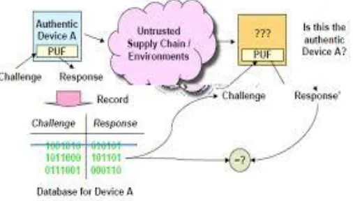
This is one of the main applications for the PUF which is widely used with less hardware
overhead by a challenge response protocol. As illustrated in Figure 1.1 a secure database
that stores all the set of CRPs from each PUF pair to use. When we need to check the
authenticity of the circuit, the set of CRPs are queried randomly from the database and
are applied to the PUF circuit. The response which is obtained is stored in the database
and checked whether it matches the response from the database for the IC or FPGA. If it
matches, then we can authenticate the FPGA or the IC. The important feature of the PUF
is we can use different CRPs and they all are random because of the manufacturing
process of the IC or the FPGA. Since all the circuits are not doped in the same
concentration to behave similar and give the same time delay to produce the output. We
use this property of the PUF to build authentication for the device[17]. It is needed to
have a strong PUF for authentication as we can have a lot of CRPs for authentication.
Figure 1.1 Schematic of Low-Cost Authentication
1.4.2
Secret Key and Random Number Generation Using PUFs
Modern Cryptographic Primitives need the essentials for generating the random number
and secret key for the message authentication and secret key generation. The use was
proposed in [14] for the use of PUF responses as secret keys and it needs to be ensured
4
because of noise and environmental conditions so we need some error correction
processes. During this process an error syndrome is evaluated when the challenge is
applied, and this syndrome is used when its being used for reconstruction of the PUF
response which might have some errors due to noise and environmental variations. After
computing and evaluating the PUF response we hash the response, so we get the secret
key that can be used officially for authentication. The most important part is we need to
generate the random numbers based on this process with low area overhead.
1.5
Thesis Contributions
In this research, we proposed, designed and evaluated a PUF which gives improved
reliability and performance compared to an existing PUF. The proposed PUF was
implemented on SASEBO G-II FPGA Board. The utility of the proposed PUF was
demonstrated by using it for hardware Intellectual Property (IP) core licensing and
authentication. Hardware Trojan can be used to provide evaluation copy of IP cores for a
limited time. After that it disables the functionality of the IP core. A finite state machine
(FSM) based hardware trojan was integrated with a binary divider IP core and evaluated
for licensing and authentication applications. The proposed PUF was used in the design
of hardware trojan. Obfuscation metric measures the effectiveness of hardware trojan. A
moderately good obfuscation level was achieved for our hardware trojan.
1.6
Thesis
Organization
The organization of the thesis is as follows: Chapter 2 discusses several types of PUFs
and their properties are briefly discussed.
Chapter 3 describes shortcomings of an existing PUF called Anderson’s PUF and
describes a proposed PUF design that mitigates the shortcomings. Chapter 4 describes an
application example of the proposed PUF in hardware IP licensing and authentication.
5
CHAPTER 2
BACKGROUND
2.1 Physical Unclonable Functions
Physical Unclonable Functions (PUF) are primitives that generate unique chip specific
signatures dynamically by using the process variations in the silicon chip during fabrication.
PUFs can be classified into two types, namely strong and weak PUFs[9]. The strong PUFs can produce multiple random responses by accepting challenges as input and mapping each
challenge to a corresponding response such that we can have a record of the unique challenge
response pair and using those for authentication. On the other hand, weak PUFs generate only
limited number of responses.
Today the Internet of Things (IoT) and wireless sensor Networks (WSNs) are used in a wide
variety of applications which requires us to use some stringent evaluation to prevent malicious
access to access these devices or the system which control it. To ensure that we have a reliable
and robust authentication mechanism each device should have a fingerprint signature which can
be efficiently used for authentication. Since they are unique to each chip or device from the
process variations inherent in the silicon at the time of fabrication. Many companies which
produce the PUFs are in demand and their products are used because of high security[16]. They
are a promising innovative primitive that is used for authentication and secret key storage
without the requirement of secure EEPROMs and other expensive hardware described above.
This is possible, because instead of storing secrets in digital memory, PUFs derive a secret from
the physical characteristics of the integrated circuit (IC).
PUFs are modelled as CRP’s (Challenge Response Pairs), which means that when we give a
challenge(c) to the PUF we get a response(r). So, depending on the challenge we can we get
different response. The mathematical representation is given as:
r = f(c), where the function represents the unique property of PUF.
6
2.2 Classification of PUF
PUFs totally depend on variations in the circuit behavior. They are classified as silicon based PUFs where the PUFs are made up of digital circuits. These PUFs are used commercially which are designed and fabricated like any other Integrated circuit. Recently we use the fabric of the FPGA to make the silicon based PUFs. The other type of PUF is the non- silicon based PUF like the optical PUFs that are described in the literature [2]. But due to their limitation in integrating with the circuit design they are not used commercially. As mentioned earlier PUFs are classified into two distinct types: strong PUF and weak PUF.
2.2.1 Strong PUF
Strong PUFs are the most important and are widely used for authentication. Since they
can support enormous number of CRPs. They can be authenticated without any cryptographic
hardware devices. The requirements of a Strong PUF are as follows:
• They should be able to generate substantial amount of CRPs in fixed time interval. • It should not be feasible to clone a PUF device and make it work like the original PUF. • The responses that are generated should not reveal any details about how the internal
functionality of the PUF works.
• Responses should be reliable and stable with respect to the environment.
2.2.2 Weak PUF
Weak PUF is usually used for key storage. A weak PUF (also called as Physically
Obfuscated PUF) has a very small range such that we can have collisions with one or other
challenges that give the same response. We define the Weak PUF function as r=F(.) where F(.)
means it has only very small domain. Even though it can be used as a fingerprint to generate
cryptographic functions, the number of responses of the weak PUF is related to the number of
components subject to manufacturing variation. A weak PUF can have only some secret keys (i.e
7
2.3 Types of PUF
PUFs are designed in such a way that they can re-generate the responses later at any time.
We are going to see the most widely used PUFs all over the world in current scenario and discuss
their advantages and disadvantages.
2.3.1 Arbiter PUF
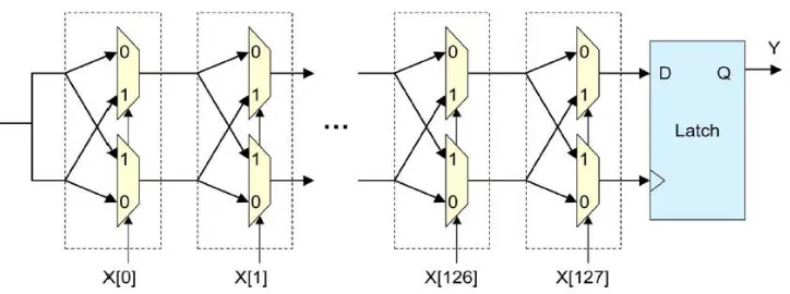
Silicon implementations of strong PUFs were described in the literature beginning in
2002 using manufacturing variability in gate delay as the source of unclonable randomness.
In one implementation, a race condition is established in a symmetric circuit. This is
shown in Fig. 2.5. An input edge is split to two multiplexors (muxes). Depending on the input
challenge bits (x[0] - x[127]), this path will vary. Although the layout is identical (propagation
time should be the same for each edge no matter what challenge bits are chosen), manufacturing
variability in the gate delay of each mux will result in one edge arriving at the latch first, and the
latch acts as the ‘‘arbiter.’’ The output will, therefore, depend on the challenge bits.
In Fig. 2.5, there are 128 challenge bits and one response bit. Of course, one typically
operates multiple identical circuits in parallel to achieve 128 response bits. In this way, the
8
Figure 2.1 Schematic of Arbiter PUF
The security of the arbiter PUF is based on assumptions regarding manufacturing
capabilities and ultimately metrology of the individual gate delays. Because the design is
symmetric, the design does not contain any ‘‘secret’’ information. An adversarial manufacturer
that has the PUF design cannot manufacture a duplicate PUF, because the behavior of the PUF is
defined by the inherent variability in the manufacturing process. Even the original manufacturer
of the PUF could not produce two identical PUFs, since this would require a significant
improvement in manufacturing control.
The second security assumption is that the individual gate delays are difficult to measure
directly. It assumes that an invasive attacker would have difficulty in extracting the individual
delays even with physical access. This assumption is based on the hypothesis that an invasive
attacker would destroy the gate delay properties using his/her measurement techniques.
The last security assumption is that given a set of CRPs from an arbiter PUF, an
adversary could not calculate the internal delays of the gates. For the architecture described
above, this is not the case. Each delay is independent from all other delays, and the delays add
linearly. As a result, one can use standard linear system analysis to intelligently gather data about
the gate delays from the response bits.
Finally, in both optical and arbiter PUF architectures, it should be noted that
environmental factors play a significant role. For the optical PUF, calibration of the input
location is a concern. In the case of the arbiter PUF, one can easily recognize that environmental
variations such as temperature, supply voltage, aging, and even random noise will affect the
delay of each edge through the arbiter PUF. In addition, if the delays are close enough, the
9
error-correcting techniques are used to increase the stability of the PUF while maintaining its
security.
The initial implementation of silicon PUFs had known security issues since the delays
were linearly added to produce the resultant response bit.As a result, they could be learned with
relative ease. This issue naturally led to the introduction of other ‘‘nonlinear’’ effects to make
such modeling attacks more difficult. These efforts included xor arbiter PUFs, lightweight secure
PUFs, and feedforward arbiter PUFs.In a xor arbiter, multiple arbiter PUF outputs are xor’ed to
form a single response bit. This is shown in Fig. 2.6 These structures have shown greater
resilience against machine learning attacks.
Figure 2.2 Arbiter PUF Circuit Topology
2.3.2 Ring Oscillator PUF
The manufacturing variability intrinsic to circuit gate delay can also be used to instantiate
a ‘‘ring-oscillator PUF’’. This PUF architecture contains N identically designed ring oscillators
synthesized onto a field-programmable gate array (FPGA) or an application-specific integrated
circuit (ASIC).
Due to the variation in delay of the inverters in the ring oscillator, each will have a
slightly different frequency. The frequencies of two oscillators are measured and compared to
reveal one of the PUF output bits. If there are N oscillators, there are N(N-1)/2 possible pairings.
However, the number of output bits is limited due to correlations (if ring oscillator A is faster
than B, and B is faster than C, then clearly A is faster than C). For N oscillators, there is a
10
variation dominates, then each of these N! orderings are equally likely. Therefore, there are a
maximum of log(N!) bits that can be extracted from the PUF.
Note that the ring-oscillator PUF is a weak PUF, since there are a limited number of
‘‘challenge bits’’ that can configure the PUF’s operation. Once fabricated, the ring oscillators’
frequency is set, so the output bits of the PUF will always remain constant. Because the
ring-oscillator PUF measures differences in gate delay like the arbiter PUF, the ring-ring-oscillator PUF is
susceptible to the same set of environmental variations and noise sources. Therefore, error
correction will be equally important in this application.
In this architecture, several oscillator PUF banks are instantiated, with each oscillator
bank comprising 2k ring oscillators. A k-bit challenge is applied to each bank, to determine
which oscillators correspond to the top delays, and which oscillators correspond to the bottom
delays. The top and bottom rows are summed to produce x and y, respectively. These values are
used to produce a single bit PUF output and associated ‘‘soft-decision’’ information
corresponding to a PUF challenge. Specifically, the output bit is the sign of x–y.
Figure 2.3 Working of RO PUF
2.3.3 SRAM PUF
Both the arbiter PUF and the ring-oscillator PUF ultimately depend on variations in the
propagation delay of gates. However, this is not the only physical property on which a PUF can
be built. A popular weak PUF structure exploits the positive feedback loop in a SRAM or SRAM
11
positive feedback to force the cell into one of these two states and, once it is there, prevent the
cell from transitioning out of this state accidentally.
A write operation forces the SRAM cell to transition toward one of the two states.
However, if the device powers up and no write operation has occurred, the SRAM cell exists in a
metastable state where theoretically, the feedback pushing the cell toward the ‘‘1’’ state equals
the feedback pushing the cell toward the ‘‘0’’ state, thereby keeping the cell in this metastable
state indefinitely. In actual implementations, however, one feedback loop is always slightly
stronger than the other due to small transistor threshold mismatches resulting from process
variation. Natural thermal and shot noise trigger the positive feedback loop, and the cell relaxes
into either the ‘‘1’’ or ‘‘0’’ state depending on this process variation. Note that since the final
state depends on the difference between two feedback loops, the measurement is differential.
Therefore, common mode noise such as die temperature, power supply fluctuations, and
common mode process variations should not strongly impact the transition.
Like other strong and weak PUF implementations, the SRAM PUF is also sensitive to
noise. If the two feedback loops of the SRAM cell are sufficiently close, then random noise or
other small environmental fluctuations can result in an output bit flip. Therefore, error correction
of this output will be necessary.
Like the ring-oscillator PUF, the architecture of the SRAM PUF can be used to make
intelligent decisions regarding error coding. The key recognition is that the relative strengths of
the two feedback loops in a SRAM cell are relatively static. A cell strongly biased toward ‘‘1’’
or ‘‘0’’ will remain strongly biased toward ‘‘1’’ or ‘‘0,’’ respectively.
Therefore, by using repeated measurements, one can assess the stability of a SRAM PUF output
bit and selectively use the most stable bits as the PUF output. This process is used in conjunction
12
Figure 2.4 Schematic of SRAM PUF
2.3.4 Anderson PUF
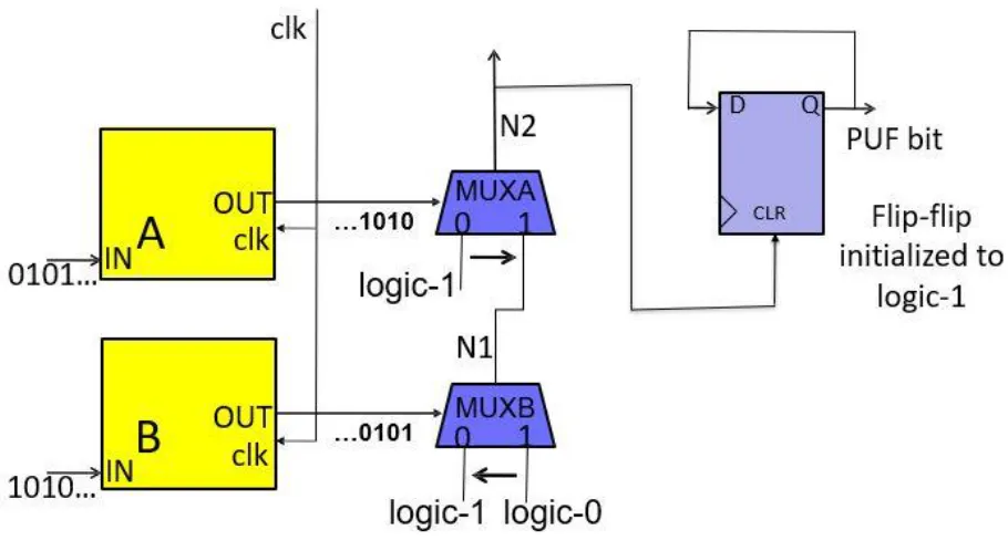
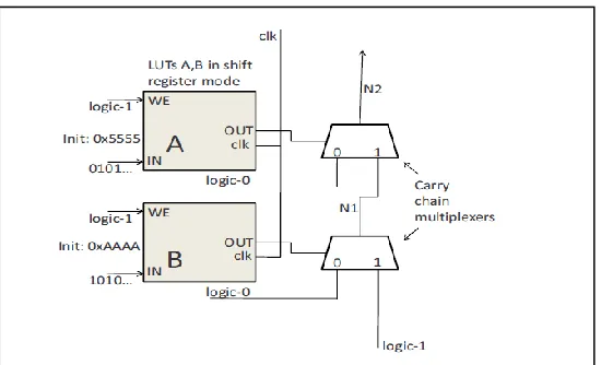
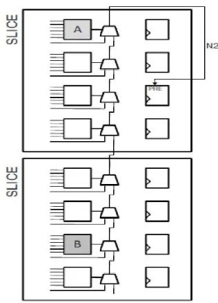
Anderson PUF is a glitch PUF which generates random signature based on the glitches
that are produced within the FPGA fabric. We design the Anderson PUF by having two shift
registers and two carry chain adders and two flip flops. We have two LUTs that generate the
opposite patterns of sequence such that as follows referred from[1].
LUT A:0101010010101010(0*5555)
LUT B:1010101010101010(0*AAAA)
13
These are the initial values for the LUTs. The IN pin makes sure that this pattern
continues every 16 cycles for the 2 LUTs and the OUT pins are used to drive the select input
pins on carry chain multiplexers. Both carry multiplexer have their ‘0’ input tied to logic-0 and the bottom carry chain multiplexer has ‘1’ data input tied to logic-1.
Consider the initial case LUTA is at logic-0 so we get N2 at logic-0. The output pin of LUT B is
‘1’. At rising edge, the OUTPUT pin of LUTA will change from logic-0 to logic-1 and the
output pin of LUT B will change from logic-1 to logic-0. Although LUT A and the multiplexer it
drives as same as the LUT B, the two pieces of circuitry in fact experience different delays due
to random process variations.
We have two cases to look upon. First case when LUT B and the multiplexer is faster than LUT
A and its multiplexer. In this case, LUT B transitions from logic 1 to 0, similarly N1 also
transitions from logic 1 to 0. Following that slower LUT A transitions from logic 0 to 1,such that
signal N2 is kept constant at logic 0 throughout the process. The second case is the opposite one
where LUT A and its multiplexer is faster than LUT B and its multiplexer. In this case, LUT A ‘s
OUT pin transitions from logic 0 to 1 and net N1 has not yet transitioned from logic 1 to logic 0.
Therefore, we have a short positive spike(glitch) will appear on N2 for the period before N1
transitions to logic-0. The presence or absence of a positive spike on N2 and the length of the
spike pulse, are due to the process variations that impact LUT A and LUT B. This variation in
N2 is used to determine the PUF signature bit. Whenever there is a glitch we get a logic-1,
otherwise it’s at logic 0. If the pulse is always generated and its width is too wide ,it’s more
likely to reach the flipflop preset input, making PUF bit ‘1’.
We need to keep in mind that the pulse width is more to create a good PUF design. For this, we
have made LUT B as far as it can so that we get a longer pulse width to be produced within the
14
Figure 2.6 Tuned PUF bit generator
2.4 Metrics for PUF Evaluation
To understand the PUFs utility as a proper authentication source, we have two different
metrics they are Intra-distance P UF variation and Inter-distance variation[2].
2.4.1 Inter distance variation
Its defined as the number of bits in a PUF response that vary between different devices
for a set of same challenges[9]. This is because every device or the chip is fabricated with
different doping levels as the doping concentration cannot be controlled at fabrication. This
15
2.4.2 Intra distance variation
Its defined as the number of bits in a PUF response that varies when the same challenge
is given to the same chip in different environmental and noise conditions. Its usually measured
as a statistical distribution. Intra- PUF variation is a measure of the reproducibility of responses
from the PUF device. Usually Intra distance PUF variation measures the reliability of the circuit.
For a secure authentication usage , Intra PUF variation should be very low( almost 0%) and the
16
CHAPTER 3
PROPOSED PUF
3.1 Limitations of Anderson PUF
As mentioned in a previous research paper, when the Andersons PUFs intra-distance
variation was measured for 90 bits, we were able to see an error of around 30 percent in
SASEBO G II (Virtex-5 FPGA )[2].The error continues over time and does not stop there. It not
only violates the basic requirement of a PUF but also makes the PUF impractical for real time
usage. When the PUF is not reliable it cannot be used for any anti-counterfeiting or IP Piracy
applications.
The reason for this is found out to be that the routing path from the output of the carry chain
multiplexers to the flip flop preset input are acting a as a low pass filter. This gives us a
convincing evidence that the glitches of short duration are not enough to trigger the preset input
of the flip flop. So that the preset input of the flip flop will always remain at 0.
Figure 3.1 shows the responses for a 320-bit Anderson PUF when measured at different points in
time. When we take the readings at a later point of time we can see that the number of bits
changing to 1 increases eventually. This tells us that the glitches that are of short duration are not
able to trigger the preset input of the flip flop. Andersons PUF is designed keeping the FPGA
fabric in mind and using the components that are there in the FPGA[6]. We should try to find a
17
Figure 3.1 Saturation test on Anderson PUF [2]
18
3.2 Recommendations to overcome the glitch effect
In this section we will see how to overcome the glitch effect for the Andersons PUF.
Here we will discuss two recommendations that can effectively mitigating the glitch effect.
3.2.1 Solution 1
This solution eradicates the glitch width transition between the bottom and the top LUT
by adding an additional carry chain[2]. The problem that was pertaining to the previous model
was there was a considerable bias towards 0. Since the glitches of short duration are damped out
before they reach their top LUT, this additional carry chain option proved to be a suitable
alternative. This implies that a trade-off between area (an additional LUT is required, per
instance, to support the extended carry chain) and flexibility(range of variation possible).
Figure 3.3 Solution 1 Saturation test [2]
Figure 3.3 shows the Hamming weight of responses from the 208-bit PUF design on four
virtual devices. The results are related to sampling the PUF at power on. We can see increased
hardware component as a result we could get only fewer testing bits. Whenever new samples
19
distance variation with the SASEBO G 2 board with better results of just 5 % with intra distance
variation.
Figure 3.4 Solution 1 Intra distance and Inter distance metrics [2]
3.2.2 Solution 2
This solution eliminates the saturation problem to latch the PUF output and can
capture a stable PUF output. Figure 3.1 shows that there is a considerable bias towards bias 0 in
the PUF response. The results tell us that there is no uniformity, so it makes the PUF unusable
for security purpose[7]. This idea gives a solution to capture the response later, so the response
gets settled uniformly without the need for key extraction. This gives us a drawback towards
20
Figure 3.5 Solution 2 Saturation Test [2]
Figure 3.6 Solution 2 Intra distance and Inter distance metrics [2]
Figure 3.5 and 3.6 gives us the Hamming weight of the responses from the 320-bit PUF design.
The results were generated after a time of 0.5 sec and then sampled and used for generating the
21
3.3 Description and Evaluation of the Proposed PUF
3.3.1 The proposed PUF
We have re-designed the Anderson PUF by changing the glitch value from active
high to active low as recommended in the previous published paper[2]. The proposed design is
shown in Figure 3.7.
Figure 3.7 One Bit Proposed PUF
The above figure interchanges the logic 0 and the logic 1 from the multiplexers value in such a
way that the we will get logic-1 when the bottom LUT works faster and we can expect a glitch
when the top LUT works faster. The other important change which we are introducing here is the
signal N2 is being connected to the Clear input to the flip flop instead of the preset input of the
flip flop. This variation is also proven to be effective in generating efficient results and a robust
design. Here, we will improve the PUF design by integrating with the solution 1( also called as
the one-shot approach) of the recommendation that was discussed earlier. This will be suitable in
22
3.3.2 Experimental Setup for Evaluation
Figure 3.8 Experimental Setup
We used a SASEBO G II FPGA Board which houses both the powerful FPGA devices the
Virtex-5 and the Spartan 3A series[18]. We used a 4 GB RAM Windows OS System with the
Xilinx ISE Software. We used the Xilinx ISE Design Suite for this research because the Xilinx
Vivado doesnot allow us to use it with Virtex-5 as it supports only higher end Virtex and the
Zynq series only.
3.3.3 Analysis of the proposed PUF
We instantiated 90 instances of our PUF design to generate a 90 Bit signature. We
evaluated the design using virtex-5 FPGA on SASEBO G2 board. The Board houses a Xilinx
Virtex-5 (XC5VLX30 – FFFG324)[5]. A total of 19200 LUT cells are available and
approximately a quarter of which can be used in shift register mode which gives ~ 4800
LUTs[2]. The board has a Xilinx Platform Connector which we used to communicate the PUF
Signature to a connected PC. We clocked the PUF using the 24 MHz clock signal available on
23
In addition to comparing PUF signatures across different FPGA chips, we can also implement a
PUF multiple times on a single chip, each time in a different region of the chip. Naturally, we
expect that any two FPGA chips should differ more than any two regions on a single chip.
Consequently, if PUF signatures for different regions on a single chip are subsequently unique.
We have convincing evidence that the signatures between chips will be at least as unique. We
investigated 4 PUF implementations, one implementation in each of the 4 regions. PUF
placement was constrained to regions using range constraints provided to Xilinx synthesis tool.
To analyze signature uniqueness, we consider the hamming distance between all PUF pairs
producing (4*3)/2 = 6 data points. If logic-0 and logic-1 were equally probable one would expect
the distribution to be clustered around an expected value of 45 bits. The average between any
two pairs is 43 which is almost equal to 45.
We divide the FPGA into four regions and evaluate the FPGA on all the four regions of the
FPGA which are mentioned here as follows in the underlying Virtex-5 architecture:
Region 1 -"X0Y0:X28Y40"
Region 2 -"X0Y41:X28Y79"
Region 3 -"X32Y0:X52Y40"
Region 4 -"X32Y41:X52Y79"
We will briefly discuss the implementation results in the next section based on these four regions
24
Figure 3.9 xc5vlx30 Virtex-5 FPGA divided into 4 regions
3.4 Implementation Results of the Proposed PUF in SASEBO G II
We evaluated the Anderson and the proposed PUF in these 4 regions of the Xilinx FPGA with
the challenge as (hex)“x11FFFFFFFFFFFFFFFFFFFFFF” and have got unique signatures for
both the Anderson as well as the proposed PUF as shown below in Figures 3.10 and 3.11 for the
region 1 in FPGA.
25
Figure 3.11 Proposed PUF result for 90 bits
The results shown in the Figures 3.10 and 3.11 gives us a convincing result that both are
producing unique responses even though the same challenge is given to them. Moreover, we
observed the results in different regions for the Anderson as well as the proposed PUF and found
that the signatures were unique. So, we can conclude that the glitches that originate are from
inside the FPGA and cannot be found easily by any common man to trace the response. When
measuring the Andersons PUF response on region 2, we recognized that the response is
fluctuating over time as follows shown in figure 3.12
26
The change in bit values here tells us that it takes some time for the PUF to settle its values
because the glitch width is not enough to trigger the flip flop. We integrate the proposed PUF
with the one-shot approach method so that the glitch gets enough time to reach the top carry
chain multiplexer. We demonstrated the experiment and have captured the responses for the
proposed PUF by overcoming the glitch effect which is shown in Figure 3.13 for the same
region.
Figure 3.13 Error Overcome by Proposed PUF
We have not only overcome the error, but we managed to get a reliable PUF by this design
model by using the proposed PUF with the one-shot approach. Now, we have plotted the design
for the intra-distance variation and got the results for Anderson and the Proposed PUF as almost
27
Figure 3.14 Intra Distance Metrics for Anderson PUF
Figure 3.15 Intra Distance Metrics for the Proposed PUF
We plotted the results for both the PUFs 90-bits and we were able to generate the average
Hamming weight for the Andersons PUF to be 35 where the smallest hamming weight was 28
and the largest hamming weight measured as 42. The average was almost to the half of the
28
maximum number of bits. Whereas for the proposed PUF we were able to generate the average
hamming distance as 34.5 with the Largest and the smallest Hamming distances as 42 and 27
respectively which is almost similar to the Andersons PUF.
3.4.1 Discussion
We conclude that the proposed PUF has generated unique signatures in all the regions of
the FPGA which is the need for the being the PUF to be random in nature so that the attacker
does not have any clue to predict the response of the PUF. We can also infer that the proposed
PUF model is reliable and can reduce the intra distance variation that was happening previously
with the Anderson PUFs model.
We know the well-known Intrinsic ID company which commercially started making
PUFs for strengthening the IoT security as well as the IP cores. Right now, the SRAM PUFs
which are used in Intel Stratix 10 are from Intrinsic ID. They integrate the PUF to the fuzzy
extractor to generate the helper data . Since the response of the PUF is usually noisy because of
environmental conditions so the fuzzy extractor helps in reconstructing the response with the
helper data. As how the major tech companies are using the PUF we can integrate the proposed
29
CHAPTER 4
HARDWARE TROJAN BASED PUF AUTHENTICATION
4.1 Finite State Machine Based Hardware Trojan
Utilization of IP cores has become a pervasive practice in today’s industry. IP
cores are vulnerable to many security threats like cloning, counterfeiting or re-marking of ICs by
many third-party vendors without the notice or permission of the IP design companies.
Many companies allow the users to use the IP for an evaluation period and afterwards they will
make it infeasible for the IP to be used[11]. Several attackers used this evaluation period to make
copies of their own design or try to do some side-channel attacks to break down the security.
Since companies cannot stop giving their IP for the evaluation period because it will depreciate
their business profits and will make them lose on improving their IP based on feedback from
users after the evaluation period.
In this chapter we will discuss a novel low-cost method for IP protection during evaluation. This
will allow the designers to embed a trojan inside the IP which cannot be traced and allows them
to fix an expiry date on the evaluation copy of the hardware IP[3][4]. This trojan is specially
crafted by the finite state machines. Hardware trojans are malicious modifications of a circuit
that can fail the functionality by extreme rare conditions. Here the trojan circuits follow a
sequence of finite state machine for the rare event to occur. The design flow in shown in figure
30
Figure 4.1 Trojan Evaluation [19]
The illegal IP would cease to work after the evaluation period like a hardware time-bomb. The
FSM trojan has low hardware overhead which makes it hard for the attackers to isolate it. We are
going to use the obfuscation metrics to evaluate effectiveness of trojan and implement
low-overhead design obfuscation techniques. Here we can give the key that is used to evaluate the
PUF such that if the PUF matches we can de-activate the trojan and make it possible for the users
to use the IP.
4.2 Operation of FSM Based Hardware Trojan
We follow this methodology for building an effective Trojan to prevent illegal usage of he
evaluation version of the Hardware IP. The three major steps are:
1. Trojan Design
2. Trojan Insertion
31
Figure 4.2 Operation of Trojan[19]
4.2.1 Trojan Design
In the first step, we will design the trojan that needs to be inserted into the IP. The trojan
should be designed to let the circuit function properly during the evaluation phase and trigger
after substantial number of clock cycles have been elapsed.
So, we are going to use FSM model of a trojan which has lots of different counters running
inside it on a global time. We should fix the state to satisfy the condition when all the
counters are run for the required clock cycles. Once the condition is satisfied the trojan needs
to be activated and its output is used to trigger the payload nodes of the circuit. We should
make sure that we use a lot of states so that it would be hard for the attackers to find the
trojan[12]. Sometimes we can also define in such a way that the states can have many
32
Figure 4.3 Trojan Design state diagram [19]
The activation time of the inserted trojan(Tactive) for the trojan state condition to satisfy.
The expected time of trojan activation(Tmean) is defined as the number of clock cycles after
which an embedded trojan is activated. For the ideal practical usage, we use 20 number of
states as minimum with Tmean=2.25*10^16 clock cycles.
4.2.2
Trojan Insertion
In the second step, we will integrate the trojan with the IP netlist once the design
phase has been completed. We need to choose trojan based on trigger and payload for the
trojan.
To determine the trojan trigger nodes, a set of random vectors are generated. The circuit is
simulated using the set of vectors and the signal probabilities of all the states are evaluated
and those which has less probability are considered as rare nodes.
To determine the trojan payload, the fanout and fanin of each internal node is evaluated
based on their sizes and a weighted normalized metric is used to distinguish their quality
which is given as [19]
33
Nodes with higher value of Pn are used for modification, so that the trojan is effective for the
given IP.
4.2.3 Trojan Obfuscation
In the last step, we need to make sure that the inserted trojan is well obfuscated so that
the adversary reverse engineer finds it difficult to trace where its hidden and cannot be
reverse engineered by FSM unrolling[10].
4.3 Metrics for Evaluation of Hardware Trojan
The computational complexity of the hardware trojan is given as[19]:
Where fi is the average cone-in size of the failing cone size of each node. F is failing nodes and
SN is failing state elements. For our design we have SN value as 2 and F valued as 2 and fi as 7.
The obfuscation metric is computed as 1383.67 for the proposed design which we are going to
see in the further section of the chapters. We can increase the number of nodes to increase the
complexity at any time keeping the rare condition to be the same as before to improve the metric.
Ideally the obfuscation metric value must be more so that it would be hard for the attackers to
isolate the trojan. The following guidelines should be followed for a well obfuscated trojan[19]:
• Forcing unreachable states on the state elements of the original circuit upon Trojan activation
increases the practical computational complexity of its detection, since the inputs of the proposed
state elements would contribute in increasing fi.
• Modification of a larger number of nodes increases F, which in turn increases the level of
obfuscation.
• Those nodes which have larger fanin cones should be preferably proposed.
• A Trojan with larger number of flip-flops increases its obfuscation level slightly because SN
34
We need to give a trade-off between design overhead and level of security achievable through
obfuscation.
4.4 Operation of 4- Bit divider IP injected with Hardware Trojan
The working model schematic of the trojan with the PUF for a 4-bit divider IP is shown below.
Figure 4.4 Block Diagram of Hardware Trojan with PUF authentication
As we see in the schematic the trojan is embedded inside the Divider IP core or any other core
for instance[16]. This trojan gets activated after a fixed amount of period has elapsed say 4
minutes is what we designed with the 24 MHz clock. This clock was routed from the spartan
35
tested. The trojan consists of 3 states as instance but can be improved further by adding
additional states to improve the complexity of the design.
Once the evaluation period is over we need to use different instances every time for the trojan, so
we can pass through the side channel attacks. Therefore, we chose PUF as the authentication
mechanism for the evaluating the IP cores.
4.5 Hardware Trojan Implementation in SASEBO G II
The hardware trojan with PUF for the 4-bit divider IP is implemented on the SASEBO G
II FPGA board. The working model is shown in the algorithmic state machine(ASM)diagram as
shown below.
Figure 4.5ASM for TrojanModel
S <-‘1’
Clk_count <- Clk_count+1
If clk_count =7200000
0
Clk_count <-0
false true
go
S4
Clk_count <- Clk_count+1
If clk_count =7200000
0
Clk_count <-0
false true
S5
36
Clk_count <- Clk_count+1
If clk_count =7200000
0
S=0 Clk_count <-0
false true
S6
If
response = "0011"
Fmin=1 Fmin=0
true false
37 TRUE
RR
0
C
3
S0
Start
RA
Dividend
RB
Divisor
0
1
RR||RA
Shl RR || RA
S1
C
C
-
1
S2
IF S=1 OR FMIN=1
RR <-0
RQ <- 0
38
RR >=
RB
RQ
Shl RQ|| 0
RQ
Shl RQ|| 1
RR
RR
-
RB
False
True
C = 0
S1
False
Done
Q
RQ
R
RR
S0
39
The above ASM chart described tells us that the 4-bit divider IP with the hardware trojan
embedded and the PUF is also there which is used for authentication. Once the evaluation period
is over, the trojan is triggered and made to set the quotient and the remainder to zero. If the user
needs to continue the evaluation period, they need to have suitable challenges to de-activate the
Trojan and to use the IP again with its functionality.
4.6 Experimental Results and Discussion
4.6.1 Experimental Results
The results were recorded on the Chipscope tool and the same experimental setup was
used which was discussed in Chapter 3 for the proposed PUF. When the following algorithm was
followed in a VHDL code and implemented on the SASEBO G II Board. We got the following
results as shown. This is just for test purposes and it can be improved by adding different
counters and many states to its design to increase its complexity and to increase its Obfuscation
metric values.
Figure 4.6 shows us that when we run the VHDL code we were able to generate the output of
quotient as 5 and remainder as 0 when the first Go signal has been triggered with dividend and
40
Figure 4.8 Divider IP generating response on evaluation period
Since we could not accommodate lot of I/O pins we hardcoded the first three bits of the dividend
as”111” and the 0th bit is given as trigger to control. Similarly, we hardcoded the divisor as “001”
and the 0th bit is used as a controlling bit similarly.
After the evaluation period is over, we do not get any output as the trojan got activated and
triggered the divider IP to lock. This trigger has made the divider IP to lose its functionality and
41
Figure 4.9 Divider IP stopped working after the evaluation period
42
Figure 4.10 Divider IP started working again after PUF authentication
4.6.2 Discussion
We have successfully made the working model and have demonstrated and tested it in the FPGA Board. This Trojan is not well hidden, but it can be made well hidden by increasing the number of states of the FSM and running many different counters inside them. Thus, we
conclude that we have not only presented a low-cost approach for protecting evaluation version of the hardware IPs but we have also presented a low-cost authentication scheme using PUF to unlock and re-activate the functionality of the IP. This technique can be combined with other methods like key based IP locking to achieve comprehensive IP security. We can use it
commercially by using the symmetric key encryption mechanism for exchanging the challenges and giving it to the PUF. We can also use hash functions to distort the challenges even more for producing more reliable and trusted encryption mechanism.
43
CHAPTER 5
CONCLUSION
We have proposed an improved model of PUF and have produced a reliable mechanism
by the one-shot approach method. We also got signatures which were random when testing in
different areas of the FPGA. This proposed PUF design has an improved intra-distance variation
error of 5 percent when compared to 30 percent in the Anderson PUF.
We have also made a hardware trojan which is authenticated with the proposed PUF.
This hardware trojan model is used in such a way that until a certain rare condition and a certain
state is reached, the trojan will not work to disrupt IP operation. This Trojan is designed in such
a way that the divider IP will work for an evaluation time (say 1 week) and after that the trojan
will not let the divider IP work until the IP is authenticated with the PUF. This type of security
can be commercially used as it does not need any expensive cryptographic algorithms and the
hardware overhead when compared to the existing alternate algorithms is much less. Lastly, we
can conclude that this design can be used effectively used to prevent IP piracy.
We can explore how the proposed PUF design can be modifies and adapted for
44
REFERENCES
[1] J.H Anderson. A PUF design for secure FPGA-based embedded systems. In ASP-DAC,
pages 1-6, 2010.
[2 ] P. Grabher, D. Page and M. Wojcik. On the (re) design of an FPGA-based PUF,
International Association for Cryptologic Research, 2013. https://eprint.iacr.org/2013/195.pdf
[3] A. Al-Anwar, Y. Alkabani, M. W. El-Kharashi and H. Bedour, "Hardware Trojan detection
methodology for FPGA," 2013 IEEE Pacific Rim Conference on Communications, Computers
and Signal Processing (PACRIM), Victoria, BC, 2013, pp. 177-182.
[4] M. Rostami, F. Koushanfar and R. Karri, "A Primer on Hardware Security: Models, Methods,
and Metrics," in Proceedings of the IEEE, vol. 102, no. 8, pp. 1283-1295, Aug. 2014.
[5] Virtex-5 FPGA Data Sheet, Xilinx, Inc., San Jose, CA, 2007.
[6] M. Majzoobi, F. Koushanfar, and M. Potkonjak, “Techniques for design and implementation
of secure reconfigurable PUFs,”ACM Trans. on Reconfigurable Technology and Systems, vol.
2,no. 1, pp. 1–33, 2009.
[7] Jeroen Leijten, Jef van Meerbergen and Jochen Jess,“Analysis and Reduction of Glitches in
Synchronous Networks”, Department of Electrical Engineering, Eindhoven University of
Technology, The Netherlands.
[8] R. Brodersen, A. Chandrakasan and S. Sheng, “Low-Power Signal Processing Systems”, 5th
IEEE Workshop on VLSI Signal Processing, California, USA, October 1992.
[9] C. Herder, M. D. Yu, F. Koushanfar and S. Devadas, "Physical Unclonable Functions and
Applications: A Tutorial," in Proceedings of the IEEE, vol. 102, no. 8, pp. 1126-1141, Aug.
2014.
[10] R.S. Chakraborty and S. Bhunia, “HARPOON: An obfuscation based SoC design
methodology for hardware protection”, IEEE Trans. on CAD of Integrated Circuits and Systems,
Oct. 2009.
45
http://www.scdsource.com/article.php?id=170
[12] H.-C. Liang, C.-L. Lee and J.-E. Chen, “Invalid state identification for sequential circuit test
generation”, Asian Test Symposium (ATS), 1996.
[13] J. Roy, F. Koushanfar, and I. Markov, “EPIC: ending piracy of integrated circuits,” in
IEEE/ACM Design Automation and Testin Europe, 2008, pp. 1069–1074.
[14] G. Suh and S. Devadas, “Physical unclonable functions for device authentication and secret
key generation,” in ACM/IEEEDesign Automation Conf., 2007, pp. 9–14.
[15] D. Suzuki and K. Shimizu. The glitch PUF: A new delay- PUF architecture exploiting glitch
shapes. In Proceedings of the 12th international conference on Cryptographic hardware and
embedded systems, CHES’10, pages 366–382, 2010.
[16] J. Guajardo, S.S. Kumar, G.J. Schrijen, and P. Tuyls. FPGA intrinsic PUFs and their use for
IP protection. In Proceedings of the 9th international workshop on Cryptographic Hardware and
Embedded Systems, CHES ’07, pages 63–80, 2007.
[17] “Secure and energy efficient physical unclonable functions”. Masters Thesis, Sudheendra K
Srivathsa, University of Massachusetts Amherst,2012.
[18] SASEBO G II Specifications, Research Center for Information Security, National Institute
of Advanced Industrial Science and Technology, 2009.
[19] Narasimhan, S. and Chakraborty, R. and Bhunia, S. Hardware IP Protection During
Evaluation Using Embedded Sequential Trojan. IEEE Design Test of Computers, (2011)
46
VITA AUCTORIS
NAME: Siva Prashanth
PLACE OF BIRTH: Pudukkottai, TN, India
YEAR OF BIRTH: 1993
EDUCATION: Bachelor of Engineering in Electrical and Electronics
Meenakshi Sundararajan Engineering College, Anna University, Chennai, TN, India
May 2015
Master of Applied Sciences, Electrical and Computer Engineering

![Figure 3.2 Intra distance and Inter distance metrics for the 320 bit Anderson PUF [2]](https://thumb-us.123doks.com/thumbv2/123dok_us/1345478.1167400/29.612.108.516.74.286/figure-intra-distance-inter-distance-metrics-anderson-puf.webp)
![Figure 3.3 Solution 1 Saturation test [2]](https://thumb-us.123doks.com/thumbv2/123dok_us/1345478.1167400/30.612.116.564.321.577/figure-solution-saturation-test.webp)
![Figure 3.4 Solution 1 Intra distance and Inter distance metrics [2]](https://thumb-us.123doks.com/thumbv2/123dok_us/1345478.1167400/31.612.125.545.126.366/figure-solution-intra-distance-and-inter-distance-metrics.webp)
![Figure 3.6 Solution 2 Intra distance and Inter distance metrics [2]](https://thumb-us.123doks.com/thumbv2/123dok_us/1345478.1167400/32.612.84.448.367.606/figure-solution-intra-distance-and-inter-distance-metrics.webp)