ABSTRACT
QIN, HANTANG. Development of High Resolution Rapid Prototyping Method for Flexible Electronic Devices Based on Electrohydrodynamic Inkjet Printing. (Under the direction of Drs. Yuan-Shin Lee and Jingyan Dong).
This research focuses on developing micro level rapid prototyping methods to fabricate conductive patterns for low-cost flexible electronic devices. The fabrication techniques presented in the study provide significant replenishments for additive
manufacturing community by investigating metal nanoink and rapid prototyping methods for flexible substrates.
In recent years, flexible electronics and rapid prototyping both demonstrate attractive features and have been rapidly developed. However, there are two main challenges before rapid prototyping can be applied for flexible electronics: (1) how to achieve high resolution features, and (2) how to acquire micro patterns with great electrical performance on flexible substrates.
In the research, a rapid prototyping method based on electrohydrodynamic jet (e-jet) printing was developed for fabrication of flexible electronic components using silver
nanoink. Silver nanoink was first characterized in the study for patterning of sub-20 µm features by controlling input parameters with the help of material deposition mechanism and sub-micro position system.
AC-for higher resolution and pattern accuracy. The printing speed was coupled with AC-voltage frequency to neutralize charges of printed droplets by consequently printing equally positive charged and negative charged droplets. Curing process and electroless copper deposition were investigated to improve the electrical performance of printed patterns.
Development of High Resolution Rapid Prototyping Method for Flexible Electronic Devices Based on Electrohydrodynamic Inkjet Printing
by Hantang Qin
A dissertation submitted to the Graduate Faculty of North Carolina State University
in partial fulfillment of the requirements for the degree of
Doctor of Philosophy
Industrial Engineering
Raleigh, North Carolina 2016
APPROVED BY:
_______________________________ ______________________________ Dr. Yuan-Shin Lee Dr. Jingyan Dong
Chair of Advisory Committee Co-Chair of Advisory Committee
________________________________ ________________________________ Dr. Paul H. Cohen Dr. Roger Narayan
DEDICATION
To my parents, Zhaoqing Qin and Yunping Miao, who have worked very hard to support me to achieve my goal.
To my wife, Dr. Xiaolei Shi, whose sacrificial care for me and our child makes it possible for me to complete this work.
To my daughter, Charlotte Y. Qin, who is indeed a treasure for me.
BIOGRAPHY
Hantang Qin was born in 1990, in Dingtao, Shandong, China. He moved to Jinan, capital of Shandong, in 2003, and finished his high school at Jigang High School in 2008. He received the bachelor’s degree in Electrical Engineering and Automation from Zhejiang University, China in 2012. He was accepted as a 3+X student at North Carolina State University in 2011, and received his en-route master degree in 2014. He finished his Ph.D. study in Industrial Engineering in July, 2016.
Hantang's research area focuses on novel additive manufacturing processes, rapid prototyping methods and tools, and manufacturing systems based on electrohydrodynamic inkjet printing for flexible electronics and optoelectronics. The fabrication method he proposed is capable of rapid prototyping of capacitive sensor arrays using metal nanoink for optoelectronics and flexile touch screens to replace high-cost and fragile ITO films. His research interests include micro/nano fabrication, manufacturing, automation, CAD/CAM systems, 3D printing and rapid prototyping for flexible electronics, material and multi-scale fabrication based on additive manufacturing and topography optimization applications.
ACKNOWLEDGMENTS
I would like to express my sincere appreciation to my advisor, Dr. Yuan-Shin Lee and Dr. Jingyan Dong for their continuous support, guidance and encouragement throughout my academic and research work at North Carolina State University. I would like to express my deep gratitude to Dr. Paul H. Cohen, for his help and suggestions in my research and my teaching in the department. I would like to thank Dr. Roger Narayan, for his selfless support in my research. I would like to thank Dr. Cassie Castorena for serving in my doctoral dissertation committee, Dr. Harvey West and Mr. Daniel Leonard for their helps and suggestions in my research.
TABLE OF CONTENTS
LIST OF TABLES ... viii
LIST OF FIGURES ... ix
Chapter 1 INTRODUCTION ... 1
1.1 Motivation ... 1
1.2 Research objectives and scopes ... 4
1.3 Fabrication approach ... 5
1.4 Organization of dissertation ... 7
Chapter 2 LITERATURE REVIEW ... 9
2.1. Flexible electronic devices and additive printing ... 9
2.2. Electrohydrodynamic inkjet printing ... 18
2.3. Electroless copper deposition ... 22
2.4. Direct micromachining/laser ablation ... 25
2.5. Challenges to be solved ... 28
2.6. Summary ... 29
Chapter 3 RAPID PROTOTYPING BASED ON E-JET PRINTING ... 31
3.2 Fundamental study of electrohydrodynamic inkjet printing ... 36
3.2.1 Modeling of printing mechanism ... 39
3.2.2 Amplitude and frequency of AC-pulse voltage ... 42
3.2.3 Plotting speed and droplet size ... 45
3.2.4 Multi-Layer printing ... 48
3.3 Electrical characterization and post-curing ... 50
3.3.1 Effects of connectivity on conductivity ... 51
3.3.2 Effects of curing temperature on conductivity ... 54
3.3.3 Electronic components printing ... 58
3.4 Summary ... 59
Chapter 4 ELECTROLESS COPPER DEPOSITION OF PRINTED PATTERNS ... 61
4.1 Mechanism of electroless copper deposition ... 61
4.2 Electroless copper deposition on silver seeds ... 64
4.2.1 Reaction bath and agents proportion... 67
4.2.2 Effect of temperature and time on copper growth ... 73
4.2.3 Topography analysis and electrical characterization ... 75
4.2.4 Printed patterns with silver core and copper shell ... 77
4.3 Summary ... 79
Chapter 5 DEVICE FABRICATION AND SYSTEM INTERGRATION ... 81
5.2 Capacitive touch sensor ... 85
5.3 Materials and fabrication process ... 91
5.4 High-resolution printing and multi-layer printing ... 93
5.5 Sensor test circuit layout ... 96
5.6 Large scale fabrication and testing ... 98
4.3.1 Effect of number of electrodes on capacitance ... 99
4.3.2 Effects of length on capacitance ... 100
4.3.3 Effects of distance on capacitance ... 101
4.3.4 Sensitivity with finger touch ... 102
5.7 High-resolution capacitance pattern for droplet detection ... 104
5.8 Microelectrodes fabrication ... 107
5.9 Summary ... 109
Chapter 6 CONCLUSION AND FUTURE WORKS ... 112
6.1 Conclusion ... 112
6.2 Publications and presentations ... 115
6.3 Future researches ... 118
LIST OF TABLES
LIST OF FIGURES
Figure 1.1 Overall proposed fabrication approaches ... 6 Figure 2.1 (a) Bendable display [13] with text image, (b) prototype of microelectrodes arrays showing transparency and flexibility ... 10 Figure 2.2 Schematic of structures in projected capacitive touch screens: row and column stack up layers ... 13 Figure 2.3 Fabrication of conductive patterns based on PDMS stamp [32]: (a) pressing of the PDMS stamp against the silver nanowire film, (b) stamp and peeling off, and (c) pressing the stamp on receiving substrates, (d) transfer pattern onto PET film ... 15 Figure 2.4 (a) E-jet printing working at cone-jet mode using polycaprolactone (PCL) polymer ink [48], (b) meniscus of e-jet printing using silver nanoink, (c) tip of the needle used ... 19 Figure 2.5 Planar process of electroless copper deposition on electronic device fabrication [66] ... 23 Figure 2.6 Production process flow for machining ... 25 Figure 2.7 (a) Schematic diagram of laser ablation [75], (b) microgrooves on silicon wafer [76] ... 27 Figure 3.1 Schematic of electrohydrodynamic jet printing setups ... 32 Figure 3.2 E-jet printing using DC voltage on insulating materials ... 33 Figure 3.3 Mechanism of ac-pulse modulated e-jet printing on highly insulating substrate: adjacent alternative positive and negative charged droplets will neutralize residual charges on the substrate for stable printing of continuous patterns ... 35 Figure 3.4 (a) Lab setup of e-jet printing for experiment, (b) optical image of nozzle and jetting generated ... 37 Figure 3.5 (a) AC voltage signal with duty ratio of one, (b) 30-layer straight silver track with line width of 2.3 µm printed on ABF... 38 Figure 3.6 3D AFM image of printed dots ... 40 Figure 3.7 Sketches on a microscopic of (a) mechanism of falling droplets with actual
Figure 3.14 Sketches on a microscopic scale the changes that occur during sintering of silver nanoparticles ... 51 Figure 3.15 (a) 3D AFM image of single layer pattern, (b) 3D AFM image of 20 layers pattern. (c) Cross sectional measured maximum height of 60 nm for single layer pattern with an average thickness of 27 nm and line width of 5.3 µm (d) Cross sectional measured
Figure 5.9 - Effect of length of electrodes on touch sensor capacitance ... 101 Figure 5.10 - Effect of distance between electrodes on touch sensor capacitance ... 102 Figure 5.11 (a) Response time with finger touch/not touch the sensor, (b) Capacitance change due to proximity of finger with distance from 10cm to contacting ... 103 Figure 5.12 (a) (b) Schematic view of multi-layer electrodes array, (c) high-resolution
CHAPTER 1 INTRODUCTION
1.1Motivation
The advancement of flexible electronics has been expanded from development of single-crystal silicon flexible solar cell arrays to organic light-emitting diode (OLED) displays on plastic substrate for the past five decades. In recent years, the rapid development of this field has attracted significant interests of finding and applying feasible techniques for large-area electronics with applications in flexible displays, novel medical sensors, and electronic papers. The ultimate goal for flexible electronics will always be lighter, more portable, more flexible, more stable, and less expensive to manufacture compared to
traditional rigid substrate based technologies. A wide variety of materials from polymeric to inorganic materials have been used to fabricate devices on flexible media, while these varieties also encompass plenty of performance benchmarks. Electrical and mechanical characteristics of materials, system performance and processes involved to make the device will finally determine successful applications.
Finding any suitable manufacturing processes to fabricate flexible electronic devices is part of industrial engineering, not only verifying feasible concepts, but also calibration of manufacturing variables, as well as reducing cost. It is exactly the intent of this research to propose novel rapid prototyping methods for flexible electronics and validate them,
processing, chemical deposition and etching, imprinting on web by roll-to-roll manufacturing, atomic force microscopy for surface modification, additive printing, direct laser
micromachining, etc., each of which has advantages and disadvantages. But if we consider rapid prototyping of micro patterns on flexible substrate, we will find that additive printing and direct micromachining seem to be best suitable for the following reasons. First, the cost could be tremendously reduced, by simplifying fabrication steps compared with lithography or electron beam micromachining that require vacuum environment. Second, additive printing and direct micromachining are theoretically capable of printing and machining all kinds of materials, including organic conductors, semiconductors, insulators, polymers, metals, wax, etc. It is the challenge at this moment for researchers to figure out how to apply direct printing or micromachining into fabrication of devices, e.g., thin film transistors (TFT). Third, additive printing and direct micromachining are roll-to-roll compatible process, which can be adapted as high throughput process with the help of multi-heads. Fourth, additive printing and laser micromachining use device and materials efficiently, and do not require vacuum environment. Fifth, more materials become available for additive printing,
generating new opportunities. For example, metal nano ink composed of metal nano particles may reduce process temperature of printing and sintering to values acceptable for polymer substrates. They may replace traditional indium-tin-oxide (ITO) in capacitive touch screen technology.
electronics where high resolution is required. The liquid drop generated by traditional jet printing is typically greater than 20-30 µm, much larger than resolution requirements for certain applications. It’s impossible for traditional inkjet printing to print high-quality gate dielectrics or other components for flexible electronic devices. Meanwhile, the operational stability of printed devices and related mechanical and electrical performance still need to be further investigated. A main issue is calibration and process control for different ink
materials, and on different substrates. Though inkjet printing has been used in both printing etch masks for vapor deposition and direct deposition of materials, the integration of printing steps into conventional fabrication process hasn’t been realized yet. It is important to
understand the fundamental of achievable feature resolution, variables, and placement of droplets on different substrates. The mechanical and electrical properties of fabricated devices need to be tested at device level.
1.2Research objectives and scopes
The research focused on developing rapid prototyping methods for flexible electronic devices by proposing and conducting novel advanced micro manufacturing techniques to fabricate high-resolution conductive patterns on flexible substrates. The work started from the fundamental study on jet printing parameters applying electrohydrodynamic theory in the lab built platform in order to understand how these parameters correlated to one another. These parameters include frequencies and amplitudes of applied voltage, size of nozzles, and plotting speeds. Residual charge issue of traditional e-jet printing has been successfully addressed by introducing AC-pulse modulated voltage into the printing mechanism. After calibration, the electrical properties of printed patterns were investigated. Another main challenge for e-jet printing was electrical performance of printed patterns. To further improve the conductivity of printed patterns, post treatment processes were conducted. The study has investigated post curing process for printed patterns. Curing can be used for applications where high temperature was tolerated. Electroless copper deposition was adapted to
selectively grow a copper shell out of printed silver seeds. In this way, not only uniform and surface roughness can be improved, but I can also improve stability, connectivity and
selectively deposit silver ink into these grooves, helping me to better control thickness and cross section of micro wires. These works provide useful references for future research to investigate rapid prototyping of flexible electronic devices.
In summary, it is important to propose a rapid prototyping method for flexible electronic devices. The novel process or a combination of processes must be capable of fabricating high-resolution electronic components or devices that meet all functional
requirements. I investigated new flexible technologies and showed the path to industrialist by developing necessary concepts, calibration, and process control, offering them a choice of new fabrication techniques and potential applications. The novelty on additive printing and direct micromachining are challenging and beneficial to current society. Direct
micromachining and copper deposition combined with e-jet printing showed great potential to be further applied and integrated into additive manufacturing, or other mechanical and industrial science fields.
1.3Fabrication approach
As a matter of fact, because of the varieties of parameters that may potentially affect final performance of printed components, the fundamental parameter study of e-jet printing, electroless copper deposition and device testing were required before developing any micro devices. In this section, the proposed approach was introduced and discussed in details to fabricate micro patterns or micro channels on substrates. The processing parameters,
The whole fabrication is shown in Figure 1.1. The proposed processes were all compatible to roll-to-roll manufacturing and potential used as industrial manufacturing standard processes. The research focused on improving current jet printing process by introducing electrohydrodynamic theory. To achieve better electrical performance of printed conductive component, direct micromachining was proposed to pattern substrate first with micro grooves followed by selective silver nano ink deposition. Another key technique was post treatment of printed silver seeds through electroless copper deposition to form a copper shell outside silver seeds.
Figure 1.1 Overall proposed fabrication approaches
cleaning, etching, or micromachining. Direct micromachining was a process that based on laser ablation or micromachining that was capable of patterning on substrates before additive printing. In this way, the patterned grooves can help solve the low aspect ratio problems of e-jet printing. Additive printing based on e-e-jet printing could selectively deposit functional ink onto substrates. Silver nano ink was used in the work, however, there are other options such as silver nano paste, copper or gold based nano ink. Post-treatment of e-jet printed
components was also necessary for better electrical performance of printed micro patterns. It can be a simple curing process for devices with high temperature threshold, or electroless copper deposition for components with low temperature thresholds. They were discussed in details in the following chapters.
There were several research topics in this dissertation from fundamental study in e-jet printing parameters, silver nano ink to the application in flexible substrates on
micro-machined surface. The issues were organized in the following chapters and described in the following section.
1.4Organization of dissertation
This dissertation has been divided into six chapters and the remaining sections of this dissertation were presented as follows:
Chapter 3 discussed e-jet printing in details with my results of the study, which supports the feasibility of proposed techniques. A capacitive touch sensor pattern was
presented in the section to demonstrate the capability of my methods for rapid prototyping of high resolution electronic components on flexible substrates, as a potential technique to replace ITO electrodes in traditional capacitive touch screen applications.
Chapter 4 focused on improving conductivity of printed patterns. Detailed study of curing and electroless copper deposition on printed silver seeds was described.
Chapter 5 investigated fabrication technique in device level. Projected capacitive sensor was fabricated in different designs. Mechanical and electrical performance test were conducted on the sensors to demonstrate versatility of the technique in diverse applications. The capability of our methods was fully investigated for rapid prototyping of microelectrodes arrays on flexible substrates as capacitive sensors.
CHAPTER 2LITERATURE REVIEW
The chapter began with literature reviews on flexible electronics with focus on projected capacitive displays, electrohydrodynamic inkjet printing, electroless copper deposition and direct micromachining. Some critical issues of current existing techniques were discussed in the last section of this chapter. This chapter provided several important backgrounds relating to my proposed techniques and current researches related to fabrication of highly conductive features.
2.1. Flexible electronic devices and additive printing
opportunities for human healthcare systems and flexible electronics.
(a) (b)
Figure 2.1 (a) Bendable display [13] with text image, (b) prototype of microelectrodes arrays showing transparency and flexibility
Almost at the same time fifty years ago at 1960s, flexible thin-film transistors (TFT) was brought into reality by Brody when he tried to fabricate TFT on papers and showed potential applications in display area [15]. He and his group made TFTs on a wide range of flexible substrates and invented the active matrix TFT display technology by producing the world’s first active matrix liquid crystal display in the 1970s [15]. A lot of groups in research area and industry companies began focusing on large area electronic for display applications ever since. The flexible displays have expanded dramatically in the past few decades with new materials and fabrication processes proposed.
Recently, the concept of flexible electronics has been adapted into new applications and researchers have been focused on flexible displays medical sensors, wearable devices, and radio frequency identification (RFID), most of which are touch sensor based
blocked and not come back to the infrared imaging sensors. However, their design cost is high, and initial calibration is difficult and complex [17]. Acoustic touch sensors mainly include surface acoustic wave (SAW), and acoustic pulse recognition (APR) technology. These technologies all depend on some aspects of propagating mechanical waves on the surface, capturing and analyzing those waves to determine a touch position. It is difficulty to realize multi-touch for acoustic sensors, and it is limited to relative low resolution [18]. Compared to these mechanisms mentioned above, capacitive sensing represents second widely used sensing method. Touch activity is identified by detecting minor changes in electrical current generated by contact with a finger or changes in electrostatic capacity. Substrates for capacitive touch sensors may be glass or flexible polymers, or combination of them. [19] They are usually constructed both as narrow stripes of conductors. Interdigitated electrodes are among the most commonly used structures. The change in capacitance caused by proximity of finger near an intersection is 1pF or less, and effect on adjacent electrode may be less than 0.1 pF. [20] The analysis of capacitance changes at or near intersections of electrode reports the touch action if change in capacitance exceeds the system threshold. Capacitive sensors shows excellent sensitivity with activation, and they are unaffected by most contaminations.
sensor arrays (usually glass separator with indium tin oxide deposited on both sides), and bottom LED/LCD screen [12], as shown in Figure 2.2. Projected capacitive technology shows advantages such as multi-touch, excellent optical properties, and long life. Projected capacitive touch sensors are easy to be integrated into systems using scanning algorithm, which eliminates coordinate drift and complicated calibration for display [22]. Projected capacitive touch sensors can be adapted into both glass and plastic, allowing them to have the flexibility to be contoured. Most touch applications are immune to most chemicals and extreme temperatures because sensors are usually sealed to meet the requirements.
Figure 2.2 Schematic of structures in projected capacitive touch screens: row and column stack up layers
surfaces by physical vapor deposition, electron beam deposition, or sputter deposition techniques, which are all costly layer deposition processes that require vacuum. Second, indium tin oxide (ITO) is currently the most popular material as transparent electrodes for optoelectronic devices because of its good electrical conductivity and optical transparency. However, indium is scarce resource on earth. On the other hand, its high mechanical fragility makes it hard to be used for flexible electronic devices. As a result, the demand for
alternative electrodes that can replace ITO has been critical. There are many materials that have been introduced, including carbon nanotubes [23-25], graphene [26, 27], conducting polymers [28, 29], and metal nanoink. Among them, metal nanoink has drawn attention because several advantages over other materials.
Metals possess highest conductivity among all other materials at room temperature due to their high free-electron density. At the same time, ultra-thin and ultra-small metal patterns demonstrate decent optical transparency at micro and nano scale. Transparent thin metal film and metal grids have been reported in optoelectronic devices where light must pass through while current or voltage needs to be applied as a replacement of ITO [30, 31]. The properties of these transparent metals are extremely important for device performance. For example, the brittleness properties of electrodes are crucial for flexible devices. The optical transparency and electrical resistance are another two most important parameters. To achieve the highest performance in optical transparency and resistance, metal-based
(a) (c)
(b) (d)
Figure 2.3 Fabrication of conductive patterns based on PDMS stamp [32]: (a) pressing of the PDMS stamp against the silver nanowire film, (b) stamp and peeling off, and (c) pressing the stamp on receiving substrates, (d) transfer pattern onto PET film
There are several approaches that have been reported where metal nanowire ink was used to fabricate transparent conductive electrodes. Lee et al. demonstrated
nanoink. However, the silver nanowires required a relative high annealing temperature [33], and there were poor adhesion problems [34]. The inevitable extra fabrication of PDMS stamps also increased cost of the process, and reduced the flexibility of fabrication, making it impractical for rapid prototyping of sensor arrays. It still remained a challenge for researchers to find out rapid prototyping method of sensor arrays for flexible optoelectronic applications.
above 30 µm in diameter. By incorporated with roll-to-roll fabrication, additive printing can definitely help to reduce process and material cost for flexible electronic fabrication to be used for wireless technology, photovoltaic, RFID and displays.
were still gaps to be filled for current technologies. Most of complex, multi-functional metal or alloy inks have to be characterized first before they can be adapted into real applications.
2.2. Electrohydrodynamic inkjet printing
In the last few years, there was a significant interest in finding feasible direct printing techniques for fabrication of micro-scale electronic devices with increasing applications in electronics, biotechnology and micro systems. The term direct printing refers to approaches where patterns or structures can be obtained directly without the use of masks, liquid etching or other variable fabrication processes. Directly printing approaches, especially those based on ink jet printing in high-resolution fabrication situation, demonstrate attractive features in their application. For instance, they have the ability to pattern directly on substrate regardless of the mechanical property of substrate, compared with other pattern method like
photolithography. Printed electronics and systems offer an attractive alternative to
conventional technologies by enabling the creation of large areas , multiple tracks and mass production at low cost [41]. At the same time, rapid control of printing trajectory with
programming based print control system offers great flexibility for the technique [40]. Direct write technologies thus are the low cost, high speed, noncontact, flexible and environmental friendly process.
resulted from the fact that the diameters of the droplets are typically bigger than 10 µm[46]. Even though with assistant technique, e.g., by combing lithography into these ink jet printing to confine the liquid flow [47], it remains a challenge to for electronics research and industry community to achieve the sub-micrometer level in fabrication process.
(a) (b) (c)
Figure 2.4 (a) E-jet printing working at cone-jet mode using polycaprolactone (PCL) polymer ink [48], (b) meniscus of e-jet printing using silver nanoink, (c) tip of the needle used
lab at NC State to fabricate 3D polymer scaffolds with sub-10 µm structures using e-jet printing.
When a liquid is supplied to a sufficiently high electrical potential, the liquid will form a stable cone at the tip of the nozzle and emits a jet on its summit. The technique that uses electric fields instead of thermal or acoustic offers some advantages of patterning compared with other direct write technologies. First, the dimension of droplets could be reduced dramatically (40 nm - 1.8 µm) using electrohydrodynamic printing to optimize physical properties of the liquid droplet by controlling parameters [51]. Second, the diameter of the nozzle used could be larger than nozzles of other jet printing techniques. This would avoid blockages of particles of liquid.
Manufacturing within electronic industry is demanding requiring smart fabrication technique for metallization and conductive micro-interconnects. Plenty of researches have been focused on metallic-organic compounds. To date, metal nanoparticles such as Au, Ag and Cu have been studied as promising functional materials for conductive inks, since they exhibited high conductivity and stability. As the size of metal particles decrease to
However, before e-jet printing can be adapted to any applications, there were still plenty of obstacles remained to be overcome. First, e-jet printing is a patterning method that uses a fine jet generated at the apex of ink cone of an electrospray in cone-jet mode [53], which are determined by experimental parameter, such as electric field, conductivity and viscosity of fluids and flow rate [54]. Numerical analysis of formulations and relationships are hard to develop among many parameters. Lee et al.(2012) have tried to propose a
formulation between droplet size, surface tension and applied voltage, but it was not suitable for jet formation situations [55]. More researches about conditions and parameters for e-jet printing needed to be conducted. Second, fabrication of filaments in micro and nano scale was attractive for applications of e-jet printing in circuit fabrication as well as biomedical fields. However, highly conductive silver tracks with such high resolution were tremendously difficult to print. Since single printed layer would be only 50 nm thick, it was necessary to print multi-layers for better conductivity. On the other hand, multi-layers would play a negative role on resolution. Smaller diameter of nozzle was another key factor for high resolution, while blockage of the nozzle was unavoidable and conductivity of the silver line would be poor with thinner thickness [56]. The fabrication technique have to be verified at device and system level to demonstrate its capability as electronic components.
resistivity [60]. Youn et al. put emphasis to make high resolution micro patterning using e-jet printing and succeeded in fabricating silver line with width down to 6 µm on silicon substrate using tilted-outlet nozzle instead of conventional nozzle [61]. Lee et. al. reported depositing silver tracks onto polyimide film by e-jet printing, obtaining conductor lines with resistivity about three times than bulk silver (0.0016 Ω·µm) but poor resolution (200 µm in width and 0.3-5 µm in thickness) [51, 62]. Besides, few researches have reported conductive silver tracks printed on highly insulating materials such as Ajinomoto build-up films (ABF).
2.3. Electroless copper deposition
Copper has been selected for interconnector in integrated circuits and electronic packages because of its low resistivity and high electro migration resistance. Electroless deposition of metals such as copper, silver, gold and nickel have been developed since 1990s and been widely used for production of fine metal patterns in printed circuits [63]. The planar process of electroless copper deposition on electronic device fabrication was shown in Figure 2.5. Photo resist was first deposited on to bottom level dielectric materials with patterns determined by etching masks. The pattern was etched on to bottom materials, followed by a deposition process that deposit catalytic metal onto whole area. The photoresist was then removed and only grooves that needed to be filled with copper was left. Copper will selectively grow into those grooves catalyzed by catalytic metal.
surface or metal seeds like silver or palladium, which functions as catalyst [64]. Selective deposition can be achieved by producing patterned catalysts. Hidber et al. reported patterning surfaces with palladium catalyst by microcontact printing of colloids, which enabled
selective copper metallization by electroless deposition on areas of surface activated by deposited colloids. They generated metallic features with sub-micron dimensions and film thicknesses greater than 1 µm [65].
Figure 2.5 Planar process of electroless copper deposition on electronic device fabrication [66]
Silver was selected in my research due to its catalytic properties, cost and good adhesion to substrates. Uzunlar et al. investigated a procedure composed of a H2SO4 surface
pretreatment, two-step Sn/Ag nano-colloidal catalyst seeding, and immersion in traditional formaldehyde electroless copper bath. The H2SO4 activated the epoxy surface for
sensitization of Sn. The tin-silver activation in the bath resulted in Sn and Ag products in form of Sn/Ag nano-colloidal catalyst for further copper deposition [67]. Dellas et al. used a frequency tripled laser to pattern silver seed lasers. They fabricated copper line with width of 150 µm, thickness of 2 µm and electrical resistivity of 0.005 Ω*µm [68]. Kao et al. reported copper plating using printed lines of nano sized silver seeds on aluminum substrates, and acquired copper film on silver tracks with width 100 µm and 200 µm, with film thickness of 3.6 µm and electric resistivity about 0.0018 Ω*µm, very close to bulk copper (0.00168 Ω*µm) [69].
Traditional electroless plating baths are typically composed of a metal salt such as metal ion sources like CuSO4 and AgNO3, chelating agent to prevent formation of undesired
compounds, and a reducing agent. The reactions are typically catalyzed only on noble metals, including Pt, Pd, Ag, Au, Rh, or Ir. The current challenges in electroless copper deposition include high cost of Pd-based catalysts.
2.4. Direct micromachining/laser ablation
The demand for micro products and micro components has been increasing in the past decades and will keep growing in the future in IT industry, medical and biomedical products. Silicon based manufacturing technologies are relatively highly developed because of the need for electronics industry. On the other hand, metals, polymers and ceramics based micro manufacturing still face plenty of challenges. It is continuously necessary to create novel fabrication methods and operational basis for industrial production of micro products. Figure 2.6 shows the production process in terms of machining. Material is processed into parts followed by assembly to product. This production flow also applies on micromachining. The miniaturization is able to proceed into micro level based on existing machining methods when the equipment precision can be improved and unit removal can be precisely controlled [70].
There are currently many types of fabrication process proposed by researchers for micromachining. The most simple and popular micromachining method is mechanical force based fabrication based on material removal from workpiece, such as cutting, grinding, ultrasonic machining, and punching. Mechanical force based micromachining directly contact the workpiece during fabrication, resulting in a better control of machining trajectory and better machined surface control. On the other hand, since this method is based on elastic deformation of tolls and/or workpiece, the machining force may affect accuracy and
machinability is limited. [71]
Another popular micromachining method is melting and vaporization based fabrication with the help of excessive heat selectively on workpiece, such as electrical discharge machining (EDM), electron beam machining (EBM), etc. These techniques have also been adapted for additive manufacturing of powders. For machining point of view, the useless section of workpieces is melted or vaporized by heat. One key element of melting based micromachining is concentration of energy for a high temperature at certain points on workpiece. One main advantage of this type of micromachining is that it can fabricate on workpiece regardless of its mechanical property such as fragility, and the noncontact feature of these techniques can help protect toll and workpiece. However, this noncontact feature also makes it hard to control final accuracy and surface roughness of final product. The heat affected zone on the parts might also be a potential problem. [72]
micromachining uses beams with very high energy which exceeds atoms binding energy of workpiece, to decompose the working material and remove them from workpiece. In some cases, the energy and removal is so high that the vaporization skips melting phase. Most commonly used power source include excimer laser and femtosecond laser. One main advantage of ablation based method compared with melting based method is that the heat affected one was reduced on the machined surface. The machining shape can have better accuracy and lesser defects. One major drawback of ablation based micromachining is the use of mask patterns during fabrication and relatively high energy cost.
(a) (b)
Figure 2.7 (a) Schematic diagram of laser ablation [75], (b) microgrooves on silicon wafer [76]
microgrooves on silicon wafer with the help of surface coating with poly(ethylene glycol) diacrylate [74, 75]. It is a continuous work in our lab to research on excimer laser for new applications, expanding from microfluidic systems and silicon wafers to polymer films and flexible electronics.
2.5. Challenges to be solved
Flexible electronics are attractive topics and have fancy applications, such as projected capacitive displays, wearable devices, and RFID. For current display technology, the expensive fabrication process cost and small-area limitations have motivate researchers to find new ways to replace traditional deposition process for fabrication and prototyping of electrical components. Indium tin oxide is currently the most popular transparent electrodes for optoelectronic applications but its high mechanical fragility and scarce resources property make it hard to be used for flexible electronic devices. It is our obligation to find out
alternative ways that can replace these traditional fabrication methods for future applications. The large area properties and polymer based substrate of flexible electronics is
against modern semiconductor technologies which focusing on minimizing area and
improving device densities. The scaling of flexible electronics has also pushed the technical and cost limits of conventional materials and device processing. A method for rapid
prototyping of conductive electrode patterns on substrates is necessary for research of low cost manufacturing process. Metals possess highest conductivity and decent optical
resistance, metal-based nanostructures need to be fabricated at micro scale while maintain their highest electrical conductivity at room temperature.
Directly printing approaches, especially those based on ink jet printing in high-resolution fabrication situation, demonstrate attractive features for rapid prototyping of flexible electronics. Direct printing shows the advantages such as noncontact, capable of depositing wide range of materials, scalable using multiple printing heads, and flexible in position. However, each of printing inks has to be characterized first before they can be adapted into real applications. Process control of e-jet printing and characterization of each ink needed to be investigated. Meanwhile, numerical analysis of parameter relationships needs to be developed. Residual charge problems and curing temperature issues need to be addressed before this technology can be adapted for rapid prototyping of flexible electronics. Device fabrication and system integration needs to be investigated to demonstrate efficiency of proposed methods. In the following chapter, a new rapid prototyping method was
proposed and investigated to address all these challenges.
2.6. Summary
to be combined together to fulfill needs. The flow in the chapter showed a roadmap of how my dissertation research was conducted.
CHAPTER 3 RAPID PROTOTYPING BASED ON E-JET PRINTING
As discussed in the literature review, e-jet printing is a promising approach to achieve higher printing resolution. The fabrication process advantages over other rapid prototyping method include: (1) ability for direct patterning, (2) better controllability, (3) cheap cost, (4) large area printability, (5) potential for mass production with multi heads. On the other hand, there are still several challenges remaining to be solved before it can be generalized. The characterization of each functional ink needs to be conducted first before they can be used for high-resolution applications, including plenty of parameters such as voltage, nozzle, plotting speed, performance test etc.
In this chapter, the fundamental study of e-jet printing using silver nanoink is investigated to verify the concept that e-jet printing has the capability to fabricate high resolution conductive patterns for flexible electronics.
3.1 E-jet printing mechanism
Figure 3.1 Schematic of electrohydrodynamic jet printing setups
trajectory of tracks. Note that the fabrication process is capable of on demand printing multi-layers on substrate by programming the movement of 3-axis stage.
In the last few years, several research works were presented on patterning of metal nanoparticles through e-jet printing on glass and silicon substrate [62, 77-80] and droplet analysis using different forms of voltage [81-84]. In the study, AC voltage was adapted because direct printing of highly conductive silver tracks on insulating materials in electronic industry would be a major application in the future. As shown in Figure 3.2, situations are different printing on insulating substrate using DC voltage, since the substrate will never transmit or neutralize any charges of droplets and inks. The charged ink accumulates on the substrate and then affected the whole electric field between nozzle and substrate. Two
scenarios happened: (1) the jet is affected by net charge of previously printed ink, resulting in deflection; (2) the jet is completely stopped, resulting in discontinuous tracks. A solution to address this problem is to use AC voltage instead of DC, so that it is possible that silver tracks can not only be printed on glass substrate but highly insulating materials.
(a) (b)
Figure 3.3 Mechanism of ac-pulse modulated e-jet printing on highly insulating substrate: adjacent alternative positive and negative charged droplets will neutralize residual charges on the substrate for stable printing of continuous patterns
Third, to acquire highly conductive micro tracks with good connectivity of printed metal particles, multilayered printing was attempted by direct placing the deposition on top of each other in the study with sacrificing of resolution.
3.2 Fundamental study of electrohydrodynamic inkjet printing
The detailed mechanism of AC-pulse modulated e-jet printing was demonstrated in previous section. I conducted a sequence of experiments to verify the concept and
characterize droplet formation regards to amplitude, frequency and duty rate of input voltage. Experiments using e-jet printing for direct fabrication of conductive silver tracks including electrical characterization were conducted and details were presented in the following sections.
Figure 3.4 (a) shows experimental setup for e-jet printing. The additive printing system is capable of on-demand printing planner and three dimension micro structures using not only conductive inks, but also polymers [39], wax materials [32], etc. The positioning system was configured to move linear in three orientations with 0.1 µm repeatability and accuracy. As shown in Figure 3 (a), the position system can be programmed to provide planar movement for substrate in X-Y direction with a displacement range of 100 × 100 mm, and up-and-down motion for nozzle in Z direction with a displacement range of 50 mm. A pneumatic syringe is able to provide pressure for e-jet printing and keep required flow rate if necessary with maximum pressure of 5 psi and 0.05 psi resolution.
made of silicon with aluminum coating outside. All electrical voltage input is programmed by signal generator (Agilent Technologies, Model 33220A) and amplified by high voltage source meter (Cole Parmer, Model 9741-50) before supplied to the electrodes.
Figure 3.4 (a) Lab setup of e-jet printing for experiment, (b) optical image of nozzle and jetting generated
The optical camera (Newport Corp.) is adapted to monitor fabrication process with a 0.5 µm resolution, as shown in Figure 3.4 (b) with illumination on the other side posting shade of nozzle and jet. From the image of the camera, I was able to identify the cone-jet working mode of e-jet printing, in accordance with the functioning mode of
electrohydrodynamic theory [12], indicating silver nanoink work well in our e-jet printing system.
experiment. The nanoink can easily produce electrode circuit with high-resolution compared with photolithography. I used silverjets purchased from Advanced Nano Product with 30~35 % solid content. The solvent is triethylene glycol monoethyl ether (TGME) with small amounts of lubricants and surfactants to prevent agglomeration between silver nanoparticles. The curing temperature is about 120~150 ºC from company’s data sheet, and viscosity is in the range of 10-1 cP. Three types of substrates used in the study are microscopic glass slides (100 mm × 25 mm × 1 mm ), and two highly insulating substrates, 1 mm thick ABF film coated on glass slides, and 1 mm thick PET film, which is one of the most widely used materials used for flexible electronics.
Figure 3.5 (a) AC voltage signal with duty ratio of one, (b) 30-layer straight silver track with line width of 2.3 µm printed on ABF
In the work, the experiments were conducted as follows. First, pulse frequency and pulse voltage amplitude were investigated to control printing process. The AC-pulse
produce a droplet, meaning printing frequency was expected to double pulse frequency. The amplitude of voltage determines electrical field to form droplets. An optimal frequency and voltage would be identified by obtaining stable nanoink jet. Second, plotting speed was characterized for continuous features of printed patterns with single layer. There was a
corresponding maximum plotting speed for each fixed input voltage. By regulating amplitude, frequency of input voltage, and plotting speed, I was able to print continuous silver tracks with best resolution. Third, electrical characterization in terms of multi-lay printing was conducted, including effect of multi-layer effect. The following section discussed curing temperature and other factors on conductivity of printed patterns in details. The resistance of printed silver tracks was measured using two point probe methods and details would be discussed in the following section.
The process characterization was performed on glass slides. After the process conditions were identified, continuous silver tracks and silver interconnectors were directly printed on to glass substrates, as well as insulating PET and ABF film. The shape and dimension of printed patterns was observed using high-resolution microscope (KH 770 from Hirox, and infinite 1 from Lumenera Corp.) and atomic force microscope (AFM) (Park Systems).
3.2.1 Modeling of printing mechanism
AFM image, as shown in Figure 3.6; (2) the volume loss of evaporated solvents during printing process is negligible; and (3) current in the meniscus is stable and proportion to voltage. During the printing process, the accumulated charges in the meniscus result in the formation of droplets. The total amount of charges in a droplet can be estimated by integral of electrical voltage and time. Based on my observation in my previous research presented in [38], the track line width turns out to be greater with an increased amplitude of voltage and a decreased frequency (increased cycle time), which means more charges accumulate during the time interval.
Figure 3.6 3D AFM image of printed dots
Figure 3.7 shows the mechanism of falling droplets and the patterns that these droplets form on the substrate. As shown in Figure 3.7 (a), once a droplet is formed, it will fall off and flatten on the substrate to form a dot. The volume of droplets and dots are equal. For a printed track width of d, we are interested in knowing what the initial drop size d0 should be. The volume of a printed droplet is found to be:
𝑉𝑝𝑟𝑖𝑛𝑡 =π × (𝑑2)
2
× ℎ (1)
where Vprint = volume of printed droplets, h = average height of printed droplets, d = diameter of printed droplets. The actual volume of a falling drop can be found to be:
𝑉𝑑𝑟𝑜𝑝𝑙𝑒𝑡 = 43 × π × (𝑑20)
3
(2)
where Vdroplet = actual volume of falling droplets, and d0 = actual diameter of falling droplets. Since the volume of the falling droplet is the same as the volume of the printed drop, one has the following:
𝑉𝑝𝑟𝑖𝑛𝑡 = 𝑉𝑑𝑟𝑜𝑝𝑙𝑒𝑡, →π × (𝑑2)
2
× ℎ = 43 × π × (𝑑0
2)
3
(3)
By rearranging Equation (3), one can find the droplet size d0 to be:
𝑑0 = 2 × √3𝑉𝑑𝑟𝑜𝑝𝑙𝑒𝑡4π
3
= √3 3 × 𝑑42 ×ℎ (4)
Equation (4) can be used to estimate the e-jet printing droplet size. Once we measure the average height and diameter of printed dot on the substrate, the actual size of falling droplet can be calculated using Equation (4).
The time between two adjacent droplets is half of cycle time of AC voltage. The maximum plotting speed can be calculated using the following equation. Assuming T is the cycle time of AC voltage, and f is the frequency of AC voltage, the maximum plotting speed vmax can be found as following:
𝑣𝑚𝑎𝑥 = 𝑇𝑑
𝑑 =
2𝑑
𝑇 = 2𝑑𝑓 , and 𝑇 = 1
𝑓 , 𝑇𝑑 = 𝑇
2 (5)
where T = 1/f, f = frequency of AC voltage, Td = T/2, Td = time between two adjacent droplets, d = diameter of printed droplets, and vmax= maximum plotting speed.
Equation (5) can be used for plotting speed control of XY stage position in the AC modulated e-jet printing process. As shown in Equation (5), the plotting speed for e-jet printing is determined by the frequency of the AC used in modulating e-jet printing process. 3.2.2 Amplitude and frequency of AC-pulse voltage
Figure 3.8 Optical image of e-jet printing working at cone-jet: the dimension of printed droplets is smaller than dimension of the nozzle
(a) (b)
Figure 3.9 (a) Printed silver tracks at different pulse amplitude, (b) Line with of printed silver tracks in regarding to pulse amplitude
The printing frequency was double pulse frequency because each positive or negative pulse will produce a droplet. This was how I solve the residual charge problems of e-jet printing by neutralizing printed charges with alternative positive and negative droplets for continuous patterning. I used a fixed voltage of 400 V, a fixed duty rate of 10%, plotting speed of 9 mm/s with different pulse frequencies to study its effect, as shown in Figure 3.10. Based on the measurement from Figure 3.10 (b), a reduced line with of printed silver tracks was observed with increasing frequency. Larger pulse frequency means shorter duration for charge accumulation with same duty cycle and amplitude of input voltage, thus generating a smaller droplet. It was noticed that when frequency was larger than 1000 Hz, discontinuous pattern was formed because duration time was too short for charge accumulation. It was the balance between amplitude and frequency that generated best resolution with continuous features. With fixed pulse amplitude of 400 V, frequency of 1000Hz, and duty rate of 10%, I was able to print stable continuous silver tracks with smallest line width. These parameters were adapted in the following experiments.
380 400 420 440 460
5 7 9 11 13 15 17 19 21
Am p li tud e (V )
Figure 3.10 (a) Printed silver tracks at different pulse frequencies, (b) Line width of silver tracks in regarding to pulse frequency.
3.2.3 Plotting speed and droplet size
Based on the measurements of printed silver droplets, I was capable of calculating and analyzing the mechanism of printing process. One assumption is that the falling droplets are perfect sphere and printed dots are cylinder shape with average height and diameter measured from AFM image. I assumed that the triethylene glycol in the droplets would be volatilized during falling. During the printing process, the accumulated charges in the
meniscus will result in formation of droplets. Assuming the current in meniscus is stable and proportion to voltage, the total amount of charges in a droplet can be estimated by integral of electrical voltage and time. In accord with my previous research [85-87], line width turned out to be greater with increased amplitude of voltage and decreased frequency (increased cycle time), which means more charges accumulate during the time interval.
With our previous analytical model, I was able to characterize plotting speed and estimate droplet size on single layer printing process. Using Equations (1) to (5), one can find
0 500 1000 1500
5 7 9 11 13 15 17 19 21
F re q u en cy (Hz )
the maximum e-jet printing plotting speed vmaxand the actual droplet size d0for the process, shown as follows:
𝑓 = 1000 𝐻𝑧, 𝑑 = 6.06 𝜇𝑚 , ℎ = 30.73 𝑛𝑚 Using the process parameters and Equation (5), the maximum e-jet printing plotting speed vmax can be found as follows:
𝑇 = 1𝑓 , 𝑇𝑑 = 𝑇2 , 𝑣𝑚𝑎𝑥 = 𝑇𝑑
𝑑 =
2𝑑
𝑇 = 2𝑑𝑓 = 12.12 𝑚𝑚/𝑠
By using Equation (4), the droplet size d0 can be found as follows:
𝑑0 = 2 × √3𝑉𝑑𝑟𝑜𝑝𝑙𝑒𝑡4π
3
= √3 3 × 𝑑42 ×ℎ = 0.92 𝜇𝑚
As shown in Figure 3.11, the cross section of printed silver dots has an average height of 30.73 nm and an average line width of 6.06 µm. By using Equations (4) and (5), the maximum speed vmax for connective silver tracks was 12.12 mm/sec, and the actual diameter of falling droplets was 0.92 µm. The ratio of diameter of nozzle and diameter of falling droplets was about 7.6.
According to Figure 3.11, the cross section of printed silver dots had an average height of 30.73 nm and an average line width of 6.06 µm. Based on equations (1) and (2), The maximum speed for connective silver tracks was 12.12 mm/s and the actual diameter of falling droplets was 0.92 µm, as calculated in equation (3). The ratio of diameter of nozzle and diameter of falling droplets was about 7.6.
Figure 3.12 Effect of plotting speeds: plotting speed increased from 7.5 mm/s to 16.5 mm/s with reduced line width and discontinuous pattern
Plotting speed determines droplet spacing and overlap when all other parameters were kept constant. Figure 3.12 showed printed patterns from discontinuous silver dots to
acquire stable and continuous silver tracks during my experiments. As the plotting speed increased, the width of silver tracks reduced gradually because of excess ink accumulation along printed silver tracks, as shown in Figure 3.12 with plotting speed increased from 7.5 mm/sec to 10 mm/sec. Two adjacent droplets had to have a minimum overlap in order for continuous patterns. As observed from experiments, with high plotting speed (13.5 – 16 mm/s), there was no or not enough overlap between two adjacent droplets, thus resulting in discontinuous patterns. Though some of droplets were connected, the overall continuity was interrupted. The results helped to prove that the maximum speed for connective silver tracks was about 12.12 mm/sec in this scenario based on Equations (5).
3.2.4 Multi-Layer printing
During the depositing process, the substrate was scanned over a distance of 50 mm for single layer and stable multi-layer printing in order to study the effect of connectivity on electrical performance. To achieve good conductivity of direct printing trackers, the
connectivity is an important factor that needs to be controlled. The dimension of silver nanoparticles in the ink is about 30-50 nm, encapsulated by polymer shell to avoid
coagulation. There are also certain amount of lubricants, surfactants, and solvent in the nano ink to keep it at stable suspension status. Silver nano ink will transfer from suspension status into solid status when most of solvents are evaporate. The effects of nano particle
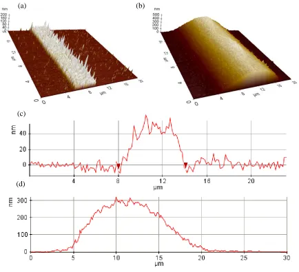
Figure 3.13 (a) Printed single layer silver track, (b) Printed multi-layers silver track, (c) Single layer pattern with average thickness of 46 nm for and line width of 5.9 µm (d) 20-layer pattern with average thickness of 187 nm and line width of 13.1 µm
Even though the silver nano ink is in stable suspension status, the viscosity of silver nano ink is relative low. As a droplet fall onto the substrate, the silver nano particles inside it will break out the surface tension and splash out. As shown in Figure 3.13 (a), single particle hillocks can be observed in single layer e-jet printed silver track. The separate existed
particle hillocks resulted in a poor connectivity condition for silver tracks. As a result, these
(a) (b)
(c)
cracks and gaps inside silver tracks would block current flow and significantly affect
conductivity of printed patterns. From Figure 3.13 (c), the maximum height for printed single layer silver track was measured to be 46 nm. It was believed that only one or two nano particles were overlaid each other considering diameter of silver nanoparticles is about 30-50 nm.
By depositing multiple layers at the same position, I can print multiple silver layers (20 layers in this example) at the track with fine semi-ellipse cross section, as shown in Figure 3.13 (b). It was clearly shown in the figure that inter-connectivity of printed pattern was improved with multi-layer printing. A maximum height of 277 nm was measured as shown in Figure 3.13 (d). However, the average line width was increased from 5.9 µm for single layer printing to 13.1 µm for multi-layer printing because there were unavoidable particles creeping down to the edge when particles stack layer by layer. For a pattern with fixed length, the corresponding resistance was inversely proportional to cross-section area of the pattern. An increased cross-section area had the ability to drive higher current and
consume lower power.
3.3 Electrical characterization and post-curing
surfactants, solvents and polymers out of silver patterns. The next step is a diffusion mechanism, where the heat will reform the silver nanoparticles, creating necks between adjacent silver particles and later transforming the necks into grain boundaries. During curing, pores and interstices will be removed once grain boundaries forms, resulting in a denser structure of printed patterns and better conductivity as well.
Figure 3.14 Sketches on a microscopic scale the changes that occur during sintering of silver nanoparticles
3.3.1 Effects of connectivity on conductivity
Figure 3.15 (a) 3D AFM image of single layer pattern, (b) 3D AFM image of 20 layers pattern. (c) Cross sectional measured maximum height of 60 nm for single layer pattern with an average thickness of 27 nm and line width of 5.3 µm (d) Cross sectional measured
maximum height of 310 nm for 20 layers pattern with an average thickness of 167 nm and line width of 15.1 µm
(a) (b)
(c)
3.3.2 Effects of curing temperature on conductivity
I compared influences of different curing temperature modalities on resistivity and morphography of printed patterns, as shown in Figure 3.16. 20-layer silver tracks were printed under the same condition where diameter of nozzle is 7 µm, frequency of voltage is 150 Hz, and amplitude is 800 volts. The first sets of samples were instantly cured at 220 ºC for 30 minutes and the result was shown in Figure 3.16 (b). The morphography indicated that silver nanoparticles went through violent crystallization, forming particle clusters when impurities inside were removed drastically in instant. The independent undulating topography resulted in poor connectivity of printed patterns and thus poor conductivity.
A ramped curing temperature modality was adapted in which the silver tracks were cured from 40 ºC to 220 ºC at 30 minutes time interval in a linear growth pattern. The
temperature was increased 18 ºC per 3 minutes in the 30 minutes time frame, and then kept at 220 ºC for 15 minutes. As we can see from the topography shown in Figure 3.16 (a), the ramped curing temperature led to a smooth diffusion and curing process for silver tracks. The ramped temperature modality was adapted in the fabrication process for the following
Figure 3.16 (a) 3D AFM image of 20 layers pattern cured with ramped temperature to 220 ºC, (b) 3D AFM image of 20 layers pattern cured instantly to 220 ºC
A contacting two probes method was adapted for measurement of resistance of printed silver patterns. An ohmmeter (Fluke) would detect the resistance when two contact probes were placed at two ends of silver tracks in a fixed length. The resistance of printed patterns can be calculated using Equation (6).
𝑅 = 𝜌 × 𝐿 / 𝐴 (6) where R = resistance of printed silver tracks, 𝜌 = resistivity of printed silver tracks, A = area of cross-section of printed silver tracks, and L = length between the two contact probes.
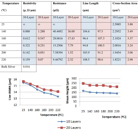
To find the effect of curing temperature on resistivity of printed patterns, 10-layer silver tracks and 20-layer silver tracks were printed when the pulse frequency, amplitude, plotting speed and nozzle diameter were fixed at 150 Hz, 800 V, 7 mm/s and 7 µm, respectively. Five different curing temperatures (140ºC, 160 ºC, 180ºC, 200ºC and 220ºC) were applied on 10-layer and 20-layer samples using ramped modality as shown in previous
section. After post curing, we measured each sample at five different positions and averaged for its resistance. The average cross-section area of samples was from AFM results.
Table 3.1 Electrical characterization of printed 10-layer and 20-layer silver tracks
Temperature
(ºC)
Resistivity
(ρ, Ω·μm)
Resistance
(μΩ)
Line Length
(μm)
Cross-Section Area
(μm2)
10-Layer 20-Layer 10-Layer 20-Layer 10-Layer 20-Layer 10-Layer 20-Layer
25 ∞ ∞ ∞ 2.5885 3.88
140 0.888 1.288 40.4692 36.00 104.6 97.5 2.2952 3.49
160 0.612 0.547 28.0616 17.43 96.4 107.3 2.1024 3.37
180 0.322 0.251 15.2506 7.79 94.8 100.5 2.0016 3.24
200 0.142 0.051 7.58394 1.52 103.9 91.2 1.9454 3.06
220 0.159 0.07 9.46792 2.32 108.5 98.6 1.8221 2.98
Bulk Silver 0.016
Table 3.1 and Figure 3.18 demonstrated resistivity changes and constriction of printed silver tracks with respect to curing process. Shrinkage occurs during curing process as results of pore size reduction, lubricants and surfactants evaporation. This largely depends on the composition of silver ink, temperature and time. Silver tracks were printed with 10 lays and 20 lays using the same nozzle with glass tip outer diameter of 7 µm, using an AC voltage with 130 Hz frequency and 820 volts amplitude. The silver tracks were cured under
temperatures of 140 ºC, 160 ºC, 180 ºC, 200 ºC and 220 ºC using ramped pattern. As shown in Figure 3.17, there was a reduction in both line width and mean height (similar to
maximum height) due to shrinkage. As maximum curing temperature went high, the
shrinkage was more obvious. A maximal 14.2% reduction of line width and 17.8% reduction of mean height were observed in 10 layers sample. A maximal 10.2% reduction of line width and 14.5% reduction of mean height were observed in 20 layers sample.
0 0.2 0.4 0.6 0.8 1 1.2 1.4
140 160 180 200 220
R esi st iv it y ( ρ, Ω ·μ m)
Temperature (ºC)
(a) Resistivity 10-Layer 20-Layer 1.5 1.8 2.1 2.4 2.7 3 3.3 3.6 3.9 4.2
25 140 160 180 200 220
Cr o ss -S ec tio n Ar ea (μ m* μ m) Temperature (ºC) (b) Cross-Section Area
Figure 3.18 (a) Resistivity in regard to curing temperature, (b) Shrinkage of silver tracks with a reduction in cross-section area due to curing process
From Equation (6), resistance is a product of resistivity and cross-section area with fixed line length. The geometric dimension of printed plays a significant role in electrical performance. At room temperature of 25 ºC, the line widths of printed 10-layer silver tracks and 20-layer silver tracks showed almost same line width, but the thickness was increased from 167 nm to 247 nm with 10 more layers printing. Printed patterns shrinks during curing process to get rid of impurities inside, defusing and reforming nano particles, resulting in reduction of cross-section area. With higher temperature, the deduction ratio became higher. A maximal 29.6% reduction of cross-section area was observed in 10-layer sample at curing temperature of 200 ºC. But the resistance was tremendously reduced because of improved resistivity.
Curing process improved conductivity of printed patterns, as shown in Figure 3.18 (a). The optimal temperature for curing is 200 ºC where conductivity of silver tracks reached a peak value. The minimum resistivity measured was 5.1 ×10⁻² Ω·µm, about three times than that of bulk silver at room temperature. The electrical performance of printed silver patterns was no better than bulk silver because of unavoidable voids and inter coarse network
between silver particles inside the track. 3.3.3 Electronic components printing
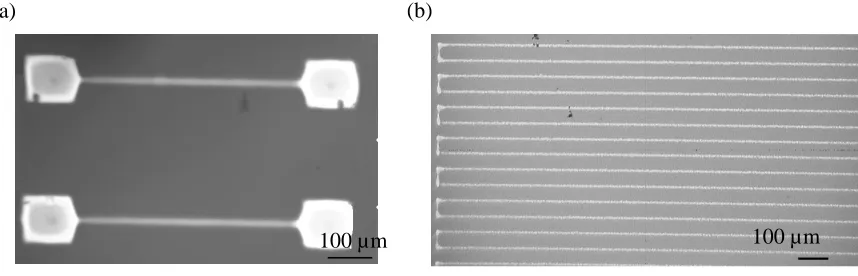
demonstrated silver tracks with line width of 12 µm printed on ABF, which was a highly insulating material. These can be applied for micro capacitor or inductor fabrication.
Figure 3.19 Printed electronic components: (a) printed metal pads and interconnects (b) an inductor
3.4 Summary
In this chapter, a novel AC-pulse modulated e-jet printing technique was developed with improved controllability, resolution and electrical performance for printed patterns. Fabrication process and detailed analytical track formation mechanism were investigated and validated experimentally. AC-pulse modulated e-jet printing alternates charge polarity of adjacent droplets to neutralize charges remained on the substrate for printing on highly insulating materials. Pulse frequency, pulse amplitude, and plotting speed can be controlled independently for continuous features with sub-10 µm resolution. Multi-layer printing technique and post curing process were applied for desired resistivity of silver tracks. It is demonstrated that the proposed printing technique can achieve both high-resolution and low
100 µm 100 µm
resistivity patterns on insulated surfaces, showing great potential in flexible electronic and printed electronic applications. The presented AC modulated e-jet technique is capable to fabricate resistors, inductors and micro interconnects, which offer a simple and versatile method to on demand direct fabricate conductive patterns in micro/nano electronic manufacturing.

![Figure 2.3 Fabrication of conductive patterns based on PDMS stamp [32]: (a) pressing of the](https://thumb-us.123doks.com/thumbv2/123dok_us/1347060.1167579/29.612.94.518.71.315/figure-fabrication-conductive-patterns-based-pdms-stamp-pressing.webp)