University of Twente
Faculty of Electrical Engineering,
Mathematics & Computer Science
The design of a new power
combining technique for
the RF power amplifiers
Wei Cheng
MSc. Thesis
May 2006
Supervisors: Prof. dr. ir. B. Nauta Dr. ir. A.J. Annnema Ms.C. M. Acar 16th,May 2006
The design of a new power combining
technique for the RF power amplifiers
by
Wei Cheng
SUBMITTED IN PARTIAL OF FULFILLMENT OF
THE REQUIREMENTS OF THE DEGREE OF
MASTER OF SCIENCE
AT
UNIVERSITY OF TWENTE
ENSCHEDE, THE NETHERLANDS
MAY 2006
University of Twente
Department of
Electrical Engineering
The undersigned hereby certifies that they have read and
recommend to the Faculty of Electrical Engineering, Mathematics
and Computer Science for acceptance of a thesis entitled “The
design of a new power combining technique for RF power
amplifiers”, by Wei Cheng submitted in partial fulfillment of the
requirements of the degree of Master of Science.
Date:
Supervisor:
Prof.dr.ir B.Nauta
dr. ir. A.J. Annnema
Ms.C. M. Acar
Content
Abstract... vi
Acknowledgement ... vii
Chapter 1 Introduction ... 1
1.1 Motivation... 1
1.2 Organization... 3
Chapter 2 Introduction on Power Combining... 5
2.1 Introduction... 5
2.2 Power Amplifier Block... 5
2.2.1 Introduction... 5
2.2.2 Linear Power Amplifier ... 7
2.2.3 Nonlinear Power Amplifier... 12
2.2.4 Summary... 20
2.3 Power Combining Network Block... 21
2.3.1 Introduction... 21
2.3.2 On-chip Power Combining Technique ... 22
2.3.3 Off-chip Power Combining Technique... 24
2.4 Summary... 26
Chapter 3 N-device Unbalanced Combining Technique ... 27
3.1 Introduction... 27
3.2 Voltage summation structure ... 28
3.2.1 New analysis for the voltage summation structure... 28
3.2.2 Limitations for the voltage summation structure... 33
3.2.3 Voltage summation or power summation... 38
3.3 Theoretical Analysis of N-device Unbalanced Combining Technique ... 44
3.3.1 Introduction... 44
3.3.2 Analysis Model ... 47
3.3.3 Design equations for the quarter-wavelength combining network... 50
3.4 Design examples ... 56
3.4.2 Simulation results of a two-device balanced combining structure ... 57
3.4.3 Simulation results of four-device unbalanced combining structure ... 59
3.4.4 Simulation results of two-device class C balanced combining structure... 64
3.5 Discussion... 67
3.6 Summary... 74
Chapter 4 Nonidealities in the N-device unbalanced combining technique ... 75
4.1 Introduction... 75
4.2 Phase nonidealities... 77
4.2.1 Introduction... 77
4.2.2 The effect of phase difference on the combination structure... 77
4.2.3 The sources of the phase nonidealities... 81
4.2.4 Methods of Phase Compensation... 90
4.3 Amplitude nonidealities... 97
4.3.1 Sources of the amplitude nonidealities ... 99
4.3.2 The effect of amplitude nonidealities ... 100
4.3.3 General mathematical model ... 100
4.3.4 Example of the amplitude difference nonidealities ... 104
4.4 Non-resistive antenna nonidealities ... 110
4.4.1 Antenna with small reactive part in parallel ... 110
4.4.2 Antenna with large reactive part in parallel... 111
4.5 Summary... 114
Chapter 5 The implementation of the microstrip combining network... 115
5.1 Introduction... 115
5.2 Choice of the microstrip... 116
5.2.1 Choice of the substrate material... 116
5.2.2 Choice of microstrip trace topologies... 117
5.3 Measurement of microstrip... 120
5.3.1 Methods of measurement and accuracy... 120
5.3.2 Calibration and de-embedding... 122
5.3.3 Measurement result... 122
5.5 Summary... 131
Chapter 6 Conclusion and future work ... 132
Reference ... 135
Appendix... 141
Appendix of chapter 2 Extended resonance technique... 141
Appendix of chapter 4... 154
Appendix of chapter 5 Choice of the microstrip... 164
Appendix 6 Measurement of microstrip lines... 177
Abstract
The wireless communication market has grown tremendously in the last decade. As a crucial block in the wireless system, the power amplifier is generally realized in dedicated and hence expensive technologies. To decrease the overall cost and size of the communication devices the power amplifier is aimed to be implemented in the mainstream digital technology: CMOS. The low breakdown voltage of the transistor in the CMOS process makes it challenging to design the power amplifier with high output power. A new power combining technique based on the parallel quarter-wavelength transmission lines has been proposed and explored to overcome this problem. By combining the output power from multiple power amplifiers the total available output power can be increased. It also has the potential for the power control application and overall reliability improvement. The simulation results of several design examples present the verification for the theoretical analysis of the proposed power combining technique.
After thorough analysis of the nonidealities of the proposed power combining technique, the practical issues regarding the microstrip implementation of the combining network are discussed. The measures to minimize the layout discontinuities of the microstrip combining network have been presented in a design example.
To my dear parents
Acknowledgement
I would like to thank Mustafa Acar and Anne Johan Annema for their valuable guideline during the project. I also want to extend my thanks Bram Nauta for his help to ensure the correctness of this project. Mr. Gerard and Henk in ICD group also gave me a lot help on the CAD and measurement. I really appreciate their kind help.
I also would like to give my thanks to Paulo Lookman and Fenno de Veries. With their company in the lab at midnight the mind is not tired and the work is not hard any more.
Chapter 1
Introduction
1.1 Motivation
The increasing market for wireless communication systems has compelled more and more research to focus on radio-frequency integrated circuits (RFIC) design. Power amplifiers (PA) are one of the most crucial components in virtually every RF circuits. Among several different fabrication processes GaAs process technology have been used successfully to build PA block such as GaAs Metal Semiconductor Field Effect Transistors (MESFET’s) and GaAs Heterojunction Bipolar Transistors (HBT’s). Nevertheless, the considerable economic benefit potential of low-cost CMOS process is playing a more and more important role in RFIC area. Besides the lower cost of the process it is advantageous to put the RF front-end on the same chip as the rest of the mobile terminal. Even the less ambitious objective of implementing the mobile terminal in a set of separate chips in the same CMOS process may achieve highly economic benefits [1.1].
However, two major limitations are associated with the design of power amplifiers using sub-micron CMOS processes, namely,
1. Low transistor breakdown voltage.
2. High energy loss of on-chip impedance transformation [1.2].
Low device breakdown voltage severely constrains the design of RF power amplifiers, as the voltage on the drain of the output device in a power amplifier can swing to more than twice the supply voltage in class A and class F and even to three and half times in class E PA as shown in Fig. 1.1. A simple calculation in the following shows the constraint on the class E PA by the low breakdown voltage. The ideal output power of a class E PA is given by [1.4]
R V
P cc
out
2
365 .
1 ×
= (1.1)
65 . 3
max V
, where Vcc is the supply voltage, Vmax is the drain voltage peak and R is the optimal load the transistor wants to see.
Fig. 1.1 Schematic of class E PA
max
V is assumed to be equal to the breakdown voltage, say, 2 volt for the 0.18 um CMOS process. Therefore, to deliver a 100 mW power the load need to convert from 50 ohm to 4 ohm.
As can be seen, the low breakdown voltage not only limits the maximum power out of the PA but also requires larger impedance transformation, which causes higher loss in the on-chip transformation network [1.3]. Since the optimal resistance the transistor needs is small the PA is more sensitive to the on-chip parasitic impedance. Additionally the lower breakdown voltage results in reliability concerns, such as long-term performance and the response to voltage surges in case of an antenna impedance mismatch [1.3].
One way to tackle the problem of low power output in the CMOS PA is to combine the small amount of output power from several PAs through a lossless or low loss power combining structure. In the combing structure each PA shares the job with others, which decreases the burden for each of them which improve the long-term reliability. For example, the heat is not concentrated in one active device.
transformation and power combining simultaneously and brings the benefits for the implementation of the
4 λ
transmission line impedance-transformation technique.
1.2 Organization
In chapter 2 two basic blocks of the power combining technique are discussed, namely, the power amplifier block and the combining network block.
In chapter 3 firstly the voltage summation structure is completely analyzed and compared with the power summation structure. As a result, the theoretical analysis of the proposed power combining technique is presented and three design examples are used for verification.
In chapter 4 the nonidealities of the proposed power combining technique are discussed, namely, phase nonidealities, amplitude nonidealities and non-resistive antenna nonidealities.
In chapter 5 the implementation of the combining network on PCB is discussed. The major issues such as the choice of the PCB substrate and layout topology, measurement of the microstrip network are discussed. At the end is given a design example of the combining network on RO4003 substrate.
Chapter 2
Introduction on Power Combining
2.1 Introduction
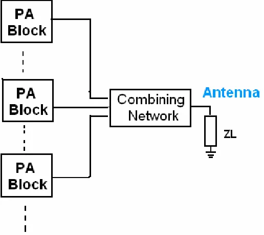
The power combining structure generally consists of two parts, namely the PA block and the combining block shown in Fig. 2.1. Through the combining network the output power produced by the PA blocks is delivered to the antenna which usually is modeled as a 50 ohm resistive load. The PA block is similar to a normal single PA except the additional influence caused by the combining structure. In the following section these two blocks will be discussed respectively.
Fig. 2.1 Block diagram of the power combining circuits.
2.2 Power Amplifier Block
2.2.1 Introduction
Fig. 2.2 Block diagram of the single power amplifier.
control block consists of a DC-feed inductor and a filtering network, which includes the transistor output capacitance . In some applications such as linear PA classes the DC-feed inductor is set to a very big value so that only DC current can pass through and the filtering network is only used to filter out the fundamental output signal. In switching PAs such as a class E PA the DC-feed inductor and the filtering network are synthesized to do the waveform shaping job. The impedance matching block is used to transfer the 50 ohm from the antenna to the optimum resistance value that the PA wants to see.
ds C
Among those four blocks the active device plays a fundamental role in the performance of the power amplifiers. Unlike in most other integrated circuits such as LNA and small-signal amplifiers, the transistors in a power amplifier do not stick on one DC point but operate in one ore more of three states; namely, off (below threshold), resistive (triode region), or current source (saturation region). Depending on which of these regions are used by the transistor, the PAs fall into two categories: linear PA and nonlinear (switching) PA. In a linear PA the transistor is supposed to operate either within the saturation region or below threshold, vGS <VTH; in a switching PA it is supposed to operate either within the ohmic region or below threshold.
Table 2.1 shows a summary of different classes of ideal power amplifiers to be discussed in the following sections, where the drain efficiency is defined as
input power DC
power output
drain =
Table 2.1 A summary of the power characteristics of different PA modes.
Class Modes Conduction
Angle
Output Power
Maximum Drain Efficiency
Linearity
A 100% moderate 50% good
AB <100% >50%
moderate <100% >50%
moderate
B 50% moderate 78.5% poor
C
linear
<50% small >78.5% poor
D 50% large 100% poor
E 50% large 100% poor
F
switching
50% large 100% poor
Fig. 2.3 shows the ideal waveform of the drain voltage and drain current of different power amplifiers, where the Y axis for the is normalized to the supply voltage [2.1]. Since the power efficiency is the primary concern in this work linear PAs will not be chosen as the PA block for the combining structure. Among the switching PAs the latter discussion will indicate that class E and class F PA are suitable for this work and finally class E will be chosen.
DS
v iDS
DS v
Fig. 2.3 Ideal waveforms of drain voltage and current of different classes of PAs.
2.2.2 Linear Power Amplifier
[2.2] and [2.5] give a classic analysis of the ideal linear PAs, which is based on three
analysis is based on. In reality the assumptions may not be fully satisfied; the impact of this is discussed at the end of this sub-section.
Ideal characteristics of linear PA
Fig. 2.4 shows the general schematic model for linear PAs, namely, class A, AB, B and
C. The inductor is set to a very large value assuming that only DC biasing current can go through from the supply voltage to the transistor . is a big capacitance to keep the dc voltage from the output. The resonant tank and together with the drain-source capacitance is resonant at the fundamental frequency so that the output current to the antenna is sinusoid.
1
L
cc
V M1 C1
1
L C2 ds
C
Fig. 2.4 General schematic for the linear PA.
All the common characteristics shared by the linear PA shown in Fig. 2.4 are listed as follows:
1. They are all biased in the saturation region and operate in the saturation and switch-off region.
2. They all use the similar harmonic control block consisting of L1, Cds, C1, L2, and C2
to filter the output current.
The only difference between them is the dc bias of the input signal at the active device gate shown in Fig. 2.5. The gate bias of the class A PA is set so that during the whole swing of input signal the transistor stays in the saturation region and the current through the transistor is a complete sinusoid waveform. In the class B PA only during half swing of the the transistor operates in the saturation region and in the switch-off region at the other half period. Thus the conduction angle and only has half part of the sinusoid waveform. In class C the dc bias of is lower than that in class B
IN v DS i IN v
o 180
=
θ iDS
and the conduction angle is less than . Class AB has the gate dc bias between class A and class B and its conduction angle is between and . Another thing that can be observed from Fig. 2.5 is that the overlap between and is decreasing as the conduction angle decreases, which mean that the class C PA has the highest drain
o 180
o
180 360o
DS
i vDS
Fig. 2.5 Time-domain waveform of the transistor. efficiency and that the class A PA has the lowest drain efficiency. Ideal assumptions of linear PAs
In fact the ideal characteristics of the linear PA above stated are based on three assumptions:
1. The transistor in the saturation region has a constant large-signal conductance
gs ds m
v i
G = , which is shown as a straight line in the iDS−vGS plot shown in Fig. 2.5. 2. The knee voltage is zero so that the drain voltage can swing in full scale from
to zero and is always larger than
DS v
cc V
2 vDS vGS −VTH so that the transistor never enters into the triode region.
3. The phase shift between and is zero and the phase shift between and is
IN
v iGS vIN
Following three practical cases will be discussed when these three assumptions are not satisfied
Practical examples when ideal-linear-PA assumptions are not satisfied
a. non-constant Gm For small-signal amplifiers the ac input is much smaller than and can be neglected so that the small-signal is constant for each fixed DC point. However, in the linear PAs the ac input is ten or a hundred times larger and the is not fixed anymore. Therefore, the straight line plot between and shown in Fig. 2.5 is just a first-order approximation for linear PAs.
gs
b. Mixed-mode PA
As can be seen in Fig. 2.5 when the approaches its peak value the is maximum and reaches its lowest value. In this region could be smaller than and then the transistor enters into the triode region. This happens more often in class C mode since the input signal needs to be larger to produce the same amount of power as in class A, AB and B modes [2.2]. In other words it shows that can not swing to zero voltage and thus the maximum swing of the output voltage is
IN
To maintain the assumption for the ideal analysis of linear PA, the input signal has to be lower so that is always larger than
IN v DS
v vGS −VTH. However, the power output is reduced and the drain efficiency is lower. Another option is to increase the input signal and make the transistor operate in a mixed mode, where the saturation and triode mode are all involved. [2.24] uses the Matlab to predict the mixed mode class C PA, however, no closed-form design equations is obtained.
IN v
Fig. 2.6 could illustrate the singe-mode and mixed-mode cases clearer. For a linear PA
1 Ideally the transistor in the linear PA stays either in the saturation region or switch-off region, therefore,
mode are all involved. [2.24] uses the Matlab to predict the mixed mode class C PA, however, no closed-form design equations is obtained.
Fig. 2.6 could illustrate the singe-mode and mixed-mode cases clearer. For a linear PA
Fig. 2.6 Comparison between the single-mode linear PA and mixed-mode linear PA. with conduction angle θ, Fig. 2.6a shows that the PA stays solely in saturation region and in the case shown in Fig. 2.6b the PA stays between the saturation and triode regions.
Fig. 2.7 Simulation result of the mixed mode class C PA shows the phase difference
c. Phase difference shifts between vIN, iGS and vDS.
Due to the drain-gate capacitance the phase difference between and at high
frequency around GHz may not be
IN
v iGS
2 π
and the phase difference between and may
not be
IN
v vDS
π, which makes the analysis of mixed-mode linear PA even more difficult. Fig. 2.7 shows the simulation result of a mixed mode class C PA2. It’s obvious that phase
difference between vIN and vDS is not π.
Summary
Normally when designing the linear PA the classic simple analysis in [2.2] and [2.5] only provides a rough initial starting point. Load-pull and source-pull simulation are often used to achieve optimum goals and avoid complex analysis involving the mixed-mode and phase shift situations.
2.2.3 Nonlinear Power Amplifier
2.2.3.1 Introduction
In contrast to the linear PAs, the active device of a nonlinear power amplifier (switching PA) is driven with a large signal input signal, turning the device on and off as a switch [2.2]. Class D, E and F are in this category. Compared to the linear PAs, the switching PAs provide higher drain efficiency. However, the output signal is not a function of the input signal any more, generally restricting these amplifiers to applications that require power amplification of constant amplitude signals [2.3]. In the following sections the class D, E, F PA will be introduced and a choice for this project will be made.
2.2.3.2 Class D Power Amplifier
Voltage-mode class-D, generally known as class-D or VMCD, implements a push-pull switching approach to amplification. Each switch is driven 180° out of phase. As shown in Fig. 2.8 when the switch M1 is on, the switch M2 is off, and vice versa.
2 The simulation result is from the class C PA which is designed in section 3.4.4 and the details can be
Therefore, the voltage is forced to be a square wave and there is no voltage-current overlap on and , resulting in a 100% drain efficiency. The filter ( and ) gets rid of the harmonics in the output current to the load. The driving signal should be a square wave with a very sharp edge in order that switches and don’t be switched on at the same time. At radio frequencies such driving signal is difficult to obtain. Besides, the device parasitic capacitance of and at point A could result in a large current-voltage overlap region during the device transition from the on to the off state and vice versa. For the VMCD the output capacitance is the dominant loss mechanism, which
DS v
1
M M2 L1 C1
1
M M2
1
M M2
Fig. 2.8 Schematic of ideal class D power amplifier and its waveform.
2.2.3.3 Class F Power Amplifier
Ideal harmonic analysis
A class F PA uses an output filter to control the harmonic content of its drain voltage and drain current waveforms, thereby shaping them to reduce the power dissipation by the transistor [2.5]. For an ideal class F PA shown in Fig 2.9a, the switch sees the optimum load
1
M R at fundamental frequency, zero impedance at even harmonics and
Fig. 2.9 Schematic of ideal class F and inverse class F power amplifier and its waveform.
class F PA [2.39] the closed-form equations couldn’t be achieved and only the numerical results are obtained using Matlab.
Like the class D PA, the dual of class F, the inverse class F PA, interchanges the voltage and current waveforms shown in Fig. 2.9b. The voltage waveform of is a half sinusoidal and is a square wave, which is enabled by the opposite harmonic terminations. Since is half sinusoid the inverse class F PA imposes higher voltage stress on the transistor and is less used when the breakdown voltage is of more concern than the maximum drain current [2.33]. However, the following discussions on the class F PA applies to the inverse class F PA.
DS v DS
i DS v
Fig. 2.10 Schematic Class F PA using the transistor as a switch.
Practical limitations
Generally the implementation of above-stated ideal class F PA faces three practical limitations:
1. The drain-source capacitance provides short-circuit termination at high harmonics. In reality the switch is usually implemented by a FET transistor (e.g. a NMOS transistor as shown in Fig. 2.10). Like for all switching PA modes the width of the transistor is very large to achieve a small switch-on resistance. As a byproduct the drain-source capacitance is large as well. Therefore, the ideal case of infinite impedance at odd harmonics is undermined in practice by the output capacitance of the transistor .
ds C
1
M
1
M
ds C
ds
C M1
at even/odd harmonics is used, where low harmonic termination value means that it is less than 13R and a high value means that the impedance is greater than
[2.1]; R
3 R is the optimum load for the class F PA shown in Fig. 2.9.
3. Infinite harmonic termination and finite harmonic termination. Sometime it’s hard to implement the harmonic termination for infinite harmonics due to the complex filter network. Instead, the class F PA with finite harmonic termination is another option, where until finite number of even/odd harmonics the short/open impedance condition is satisfied [2.6-2.7]. Based on the number of the harmonic termination the class F PA can be categorized into two groups, namely, infinite harmonic class F and finite harmonic class F.
Fig. 2.11 Infinite harmonic class F power amplifier.
Infinite harmonic class F PA
To realize zero/open at infinite even/odd harmonics the quarter-wavelength transmission line is used as shown in Fig. 2.11 [2.5]. The parallel tank and resonates at the fundamental frequency and it provides open at fundamental frequency and short at harmonics. Therefore, the drain of the transistor sees R at fundamental and zero/open at infinite even/odd harmonics. The output voltage is given by [2.7]
2
L C2
1
M
0
Z RL V v cc
o
×
=α (2.3)
, where α is the ratio between the fundamental and DC component of the drain voltage;
is the supply voltage; cc
transmission line. For the ideal infinite harmonic class F PA with square-wave drain
waveform, α is π4 .
However, as shown in Fig. 2.12 the capacitance of the transistor undermines the higher-order odd harmonic termination. A small inductor is used to tune out at fundamental frequency [2.31] to mitigate the problem. It’s trivial that the and is a parallel tank resonating at the fundamental frequency
ds
C M1
ds
L Cds
ds
L Cds
0
ω , therefore, Lds and Cds
Fig. 2.12 Infinite harmonic class F power amplifier with drain-source capacitance Cds. provides impedance
ds C N
j 2 0
1 ω
×
× at odd harmonic (2N+1)×ω0( N is an arbitrary
positive integer). Though in practice the small is absorbed into RFC, it’s plotted in Fig. 2.12 just for better illustration. Thus at higher-order odd harmonics the transistor still sees a short, which degrades the efficiency dramatically. Actually, the problem of is very severe for the transmission line infinite harmonic class F PA and there are not so many papers using this topology.
ds L
1
M ds C
Finite harmonic class F PA
area for monolithic PAs. Another advantage is that the drain-source capacitance can be incorporated in the filter network and will be no harm to the harmonic
ds C
Fig. 2.13 An example of finite harmonics class F PA incorporating Cds.
termination. Fig. 2.13 [2.26] is an example of the finite harmonic topology incorporating . In fact most of relevant papers on the class F PA are about the finite harmonic termination [2.25-2.28], [2.32] and the design of finite harmonic class F PA is similar to the filter design, which tries to realize low/high impedance at finite even/odd harmonics.
ds C
2.2.3.3 Class E Power Amplifier
The class E PA was first introduced by Ewing [2.8] in his doctoral thesis, and then was further elaborated by many other researchers [2.9], [2.10-2.13]. It also utilizes the active device as a switch, and thus can achieve high efficiency. This class uses a high-order
reactive network ( , , and ) shown in Fig. 2.14 that reduces switch losses by helping the switch voltage to reach both zero slope and zero value at the turn-on of the
1
L C1 C2 L2
switch, also known as zero voltage switching or ZVS [2.5]. As can be seen, the parasitic capacitance Cds is included in the filter network.
Time domain solutions of class E mode
Since the class E condition is in the time domain, most of the design equations are derived in time domain, which is different than in class F PA. The difference between those analysis equations is mostly in the way of switched-transistor modeling, which can be divided into three groups [1.4], [2.10-2.11] and [2.14]:
1. Zero (the switched-on resistance of the transistor ), infinite and finite ( Raab’s model). To reduce the analytical complexity [2.10-2.11] assumes the drain inductance is infinite and switch-on resistance of the transistor is zero. The filter and at the fundamental frequency is tuned to the reactance of this PA topology in the fundamental frequency is tuned to the reactance
on
R L1 jX L2
2
C
X as well. This method has the most complete model for the switch . However, only the numeric solution can be obtained.
1
M
3. Zero , finite and zero [1.4] (Andrei’s equation). This method is a compromise between the previous two models in terms of the switch modeling. It’s different from the previous two models that the filter and of this PA topology in the fundamental frequency is tuned to zero. Though this model doesn’t include the closed-form design equations has been achieved, which makes the design and optimization very convenient. Table 2.1 lists the input variables and output variables of the design equation of Wang’s and Andrei’s model. As can be seen, Andrei’s equation can not work if the load R is the input variable. As a result, the mathematical function between the output power of the class E PA and the load seen by the PA block, , can not be achieved, which supposes to be given by
Table. 2.1 The input variables and output variables calculated by the design equations of two models.
Input Variable Calculated Output
Wang’s model [2.14]
f Vcc Q L1 C1 R Pout PDC C2 L2
Andrei’s model [1.4] f
cc
V Q PDC3 R Pout L1 C2 L2
Frequency domain solutions of class E mode
[2.34] derives the optimal load for the PA at fundamental and harmonic frequency using the frequency domain analysis. This frequency domain is used especially to design the class E PA implemented by the transmission lines. Actually the impedance of the load network at fundamental frequency is equal that in Raab’s model [2.11]. Similar to the class F PA, however, it’s very difficult to realize infinite harmonic termination in a reasonable board area. [2.34-2.37] are the major papers implementing a class E PA by transmission lines and impedance termination maximally until fifth order harmonic are realized.
2.2.4 Summary
Since high efficiency of the combining structure is of prime interest in this work the linear PA modes are discarded. Due to the bad capability of handling, the class D and class F modes are not chosen, though the finite harmonic class F could incorporate it still needs more passive components than class E PA and its theoretical drain efficiency is less than 90%.
ds C
ds C
As a result, the class E mode is chosen for the combining structure in this work.
3 In Andrei’s model the power input variable is denoted as the expected power output. However, this model
2.3 Power Combining Network Block
2.3.1 Introduction
The primary requirement of a good combining network is low loss. High power loss affects the efficiency of the whole power combining system and could make the effort of combining fruitless.
Fig. 2.15 The flow chart of the power combining structure design.
As reviewed in previous section, the design equations and analysis of each PA mode is an approximation of the PA performance to some order. Therefore, to design a single PA and achieve an optimum result is already not easy, let alone designing the power combining system containing several PA blocks. The method proposed in this work is to divide the design of the whole combining system into three steps illustrated in Fig. 2.15:
1. Design the individual PA blocks separately.
2. Design the combining network according the first step.
3. Connect the PA blocks designed in step 1 with the combining network designed in step 2.
The first step is just the same as the single PA design and any previously related experience and knowledge can be used. The procedure of the second step is the focus of this work.
This design method avoids the complexity of the large system design and could save time and efforts. However, it has the following requirement on the combining network:
b. Each PA doesn’t affect the performance of any other PA in the same combining network; which is called good isolation. Since the PA blocks are designed and optimized in the first step assuming it is single, any interference caused to the PA blocks by the combining network would degrade the design expectation.
What is preferable but not necessary function is that the combining network can be a universal module for different PA modes.
There are many techniques for power combining from multiple transistors in microwave engineering. Most of these generally fall under the category of being either planar techniques or spatial techniques [2.2] [2.15] [2.17][2.38]. Spatial power combiners are 3-D structures which combine power in waveguides, or in free space. However, in RFIC design the frequency range only covers the lowest frequency spectrum of microwave engineering thus the spatial combining technique demands much more area and space than it does in the normal microwave bands, for example, higher than 10 GHz. Only the planar combining technique is of interest in this work. In the following section the planar combining technique will be divided into two classes, namely, off-chip technique and on-chip technique, depending on the way to implement.
2.3.2 On-chip Power Combining Technique
Fig. 2.16 An example of on-chip power combining technique
Limitations facing on-chip combining network
Unlike the off-chip transmission line with inherent low loss advantages the on-chip technique has to deal with two problems:
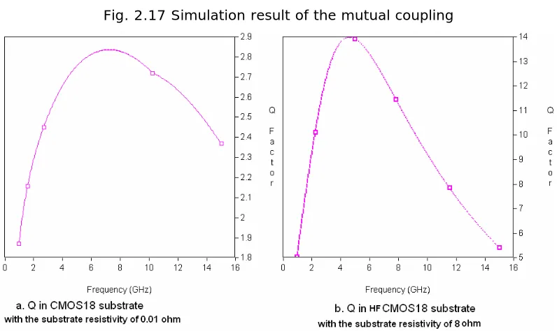
1. Low coupling factor . A simple electromagnetically-coupling slab inductor pair has been simulated in Sonnet shown in Fig. 2.17. This inductor pair is similar to the DAT structure shown in Fig. 2.16. Both the primary and secondary slab inductors are um. From the current density color it’s shown that the mutual coupling is not high.
k
8 500×
2. Low Q of passive elements. A 1000×40um slab inductor both in the normal CMOS18 process and the high-frequency CMOS18 process has been simulated in Sonnet. The results are shown in Fig. 2.17. Though the high-frequency CMOS18 process has higher substrate resistivity than the normal CMOS18 process the Q factor at 2 GHz is still around 7.
Fig. 2.17 Simulation result of the mutual coupling
Fig. 2.18 Simulation results of Q for slab inductor in two process
2.3.3 Off-chip Power Combining Technique
technique since in RFIC design the transmission line is generally implemented in low loss PCB (printed circuit board) as microstrip lines.
The Wilkinson combiner can be generalized to an N-device combiner and all ports are isolated from each other. A disadvantage is that the combiner requires crossovers of the resistors for N>3. This makes fabrication difficult in planar form [2.16], [2.17].
Fig. 2.19 Schematic example of a 3-device extended resonance power combining structure.
2.3.3.1 Extended resonance technique
One interesting method of combining power from solid-state devices was introduced, based on an extended resonance technique [2.18]-[2.20]. A standing-wave structure similar to a waveguide coupled-cavity filter is realized by resonating the device admittances with each other in order to cancel their susceptance and combine their conductance [2.18]. As shown in Fig. 2.19 the transistors M1−M3 are modeled as a
current source controlled by the signal at the gate. The transmission lines at the input and output of the transistors are designed so that the phase delay is compensated and the power output are in phase and combined in the load. Four discrete 1-W Siemens CLY5 GaAs MESFET’s with 67% power-added efficiency at 935 MHz have been combined by this technique [2.20]. A detailed analysis is given in the appendix 2.1 trying to utilize this technique. However, the extended resonance technique is based on two assumptions:
1. The input impedance of the transistor is a constant impedance and the input signal in the input branch is sinusoidal.
The input signal of the PA is large signal, especially for the switching PAs and the input impedance at the gates varies with the amplitude of the input signal and is not constant. What’s more, the transistors in the switching PAs are a switch rather than a current source. As a result, the two assumptions are undermined.
2.3.3.2 The class F PA voltage summation structure
Old analysis reviews
[2.31] uses a parallel quarter-wavelength lines to build a digital-controlled amplification system for the infinite harmonic class F PAs shown in Fig. 2.20. It claims that the switched nMOS output transistor shown in Fig. 2.20a are used as low-impedance
voltage source driving
j
transmission lines shown in Fig. 2.20b. The
low-impedance is the effective on-resistance when the transistor is driven with a large
gate-to-source input voltage and based on (2.3) is sj
the equivalent circuit shown in Fig. 2.20b the output voltage is the summation of all voltage source VMj when is very small, which is given as [2.31] rsj
As can be seen the analysis is based on two assumptions:
1. The switched transistor can be modeled as a voltage source with low source impedance.
Fig. 2.20 Schematic of the class F voltage summation structure and its equivalent circuit in [2.31]
2.3.3.3 Summary
The parallel transmission line structure shows the potential for the power combining design in this work, though a solid analysis is not available. In the next chapter a new analysis for this voltage summation structure is proposed and this structure is explored.
2.4 Summary
Chapter 3
N-device Unbalanced Combining Technique
3.1 Introduction
In this chapter the parallel transmission line structure is fully analyzed and a new power combining technique is proposed based on this structure, which theoretically can combine the output power of N arbitrary PAs. At first the parallel transmission line is explored. Secondly a theoretical analysis for the new power combining technique is presented. The simulation results to verify the theory are followed. At last a discussion and summary end this chapter
3.2 Voltage summation structure
As discussed in section 2.3.3.2, the parallel quarter-wavelength transmission line structure sums the output voltage of each class F PA shown in Fig. 3.1 (redrawn of Fig. 2.31). However, the two assumptions the analysis based on [2.31] is not solid. Due to the potential usefulness of the parallel quarter-wavelength transmission line structure, a more reasonable analysis is proposed for this voltage summation structure and a verification using simulations is given.
3.2.1 New analysis for the voltage summation structure
As shown in Fig.3.2b in the new analysis the switched transistor is modeled by an ideal switch instead of a voltage source. The supply voltage is not necessarily the same for a more general case. As introduced previously in section 2.2.3, and are DC block capacitance and DC feed inductor respectively, the parallel tank and C is assumed to be an ideal filter with high Q. Thus they are assumed to have no non-ideal effect in the summation structure and can be neglected in the following analysis.
BFC RFC
L
Analytical derivation
In fact the voltage summation structure shown in Fig.3.2b is the voltage combination of arbitrary single-stage class F PAs, which are connected directly to a load
N RLwithout
changing anything. Fig. 3.2a and 3.2b together give a good illustration. The first impression is that all the PA blocks in the summation structure will interact with each other and it’s very complex to make a full analysis for the whole system either in time or frequency domain. Therefore, a more straightforward and easier equivalent circuit shown in Fig. 3.2c is used, which can satisfy the following conditions to ensure that the equivalent circuit is the same as the summation circuit shown in Fig. 3.2b:
RL RL RL
RL1// 2//L n = (3.1)
/ /
2 /
1 o on
o
oT V V V
V = = =L= (3.2) For the ideal infinite harmonic class F PA block , any value of the load corresponds to an optimal condition, where different output power will be generated. (While for ideal class E PA there is only one optimal value for ; this difference
j
PA RLj
between ideal class E and class F PA is a key point for understanding the following analysis). The voltage output of PA block PAj of the equivalent circuit is given by (2.3)
j
Fig. 3.2 The voltage summation structure for ideal class F PAs and its equivalent circuit.
Now for the equivalent circuit in Fig. 3.2c let
0
Based on (2.3) the output voltage summation of each single-stage PA in Fig. 3.2a is given Assembling (3.4-3.6) gives
∑
voltage Vccj are the same for each single-stage class PA.(3.7) gives the combined output power of the voltage summation structure
RL
The power output summation of the voltage summation structure shown in Fig. 3.2a is given by
Comparing (3.8) and (3.9) tells that the voltage summation structure sums the voltage output of each PA block rather than the power output.
Simulation verification
A two-device voltage summation structure is simulated in ADS shown in Fig. 3.3. The voltage-controlled switch component “SwitchV”1 is used to build the ideal infinite
harmonic class F power amplifier PA1 and PA2.
Before the summation each PA is simulated in single stage. Table 3.1 shows the simulation parameters for and . Due to the non-zero switch-on resistance of the switch the drain efficiency couldn’t achieve completely 100% and the simulated voltage output for and is not exactly the same as it was calculated from 2.3. However,
1 To save the simulation time the switch-on resistance of the switch isn’t set too small. 0.05 ohm is a
Fig. 3.3 The simulation circuit of the two-device voltage summation structure.
Table. 3.1 The simulation parameters of PA1 and PA2 when they are in single stage.
1
PA PA2
cc
V (V) 3 2
RL(ohm) 50 50
0
Z (ohm) 50 100
Simulated output voltage 3.81 1.272 o
V
( V) Calculated output voltage 3.82 1.273
Drain efficiency 99.8% 99.9%
Fig. 3.4 The simulation result of the drain voltage and current waveform of and
when they are in single stage.
1
PA
2
PA
it’s reasonable to say that the and are the ideal infinite harmonic class F PA, which could also be verified by the waveform simulation result of the drain voltage and current shown in Fig. 3.4.
1
PA PA2
After putting and into the voltage summation structure shown in Fig. 3.3. The simulation results of the output voltage and power of and are listed in Table 3.2, which shows the output voltage of and are added together. At last the minor difference between the values of “summation ” should be noticed. The major reason is the minor phase difference between the output voltage of and , which is around 0.1 degree. This shows that the derived result (3.7) is valid when there is no phase difference between the output voltages to be summed. This equal-phase assumption
1
PA PA2
1
PA PA2
1
PA PA2 o V
1
PA PA2
Table 3.2 The simulation results of PA1 and PA2before and after summation. Before summation After summation
1
PA PA2 Total
Single ( V) Vo 3.81 1.272 None
Summation ( V) Vo 5.082 5.078
Drain efficiency 99.8% 99.9% 99.7%
145 16 Output power (mW)
will be discussed further in section 4.2. In summary the parallel quarter-wavelength transmission lines can provide voltage summation for arbitrary single-stage class F PAs and therefore is called voltage summation structure.
N
3.2.2 Limitations for the voltage summation structure
The general result of the voltage summation structure derived in (3.7) seems to have high potential. Within the voltage summation structure the output voltage of each PA block is summed and the combined power is even larger than the power output summation of the arbitrary single-stage class F PAs. However, (3.7) is based on the ideal transmission-line infinite harmonic class F PA with an ideal switch. In practice there are two major limitations:
N
1. Non-zero drain-source capacitance of the switched transistor 2. Non-zero switch-on resistance of the switched transistor.
Non-zero drain-source capacitance effect
As discussed in 2.2.3.3 the drain-source capacitance provides a short to the switched transistor at all high harmonics, which undermines the class F condition of “ open at odd harmonics”. Though a small inductance can tune out at the fundamental frequency, at high harmonics it still doesn’t help. To show the effect of the drain-source capacitance an infinite harmonic class F PA is simulated in ADS at 2 GHz shown in Fig 3.5.
ds C
ds C
ds C
Though the drain-source capacitance of the transistor is nonlinear the simple linear capacitance component in Fig3.5 can still show the effect on class F PA. Based on the simulation result in Cadence Spectre, the effective switch-on resistance of the NMOS transistor in Philips CMOS18 process is around 0.1 ohm when the width is 6800 um, which results a 6.3 pF effective . Thus the switch-on resistance is set to 0.1 ohm and is swept from 0 to 6 pF. The inductor is resonant with at the fundamental frequency. As shown in Fig. 3.6, though the output voltage stays almost the same, the drain efficiency drops drastically from 99.6% when is zero to 24.5% when is 6 pF. Note that even with being 1 pF the drain efficiency already drops to 63%,
ds C
ds C ds
C Lds Cds
ds
C Cds
Fig. 3.5 Simulation circuit of the infinite harmonic class F PA with parasitic
capacitance Cds.
Fig. 3.6 Simulation results of the effect on the output voltage and drain efficiency of
infinite harmonic class F PA by Cds.
meaning that a very small would degrade the infinite harmonic class F PA a lot. Finally Fig. 3.7 shows that the drain current waveform degrades from the half sinusoid and causes large overlaps with the drain voltage when is 6 pF. Since an ideal switch is used the drain voltage still keeps the square-wave shape. If a real transistor is used, the drain voltage degrades further and more overlap happens.
ds C
Fig. 3.7 Drain waveform comparisons between when Cds is 0 pF and 6 pF.
Non-zero switch-on resistance Ron
The non-zero switch-on resistance obviously reduces the drain efficiency. Even worse, it degrades the voltage summation capability for the voltage summation structure. Looking back in section 3.2.1 the analytical derivation is based on the assumption that for each PA block the output voltage, characteristic impedance and the resistive load hold
j j j oj
Z RL K V
0
×
= (3.10)
However, the non-zero switch-on resistance will invalidate (3.10), which degrades the voltage summation.
on R
Though the equation for the output voltage of the infinite harmonic class F PA including non-zero is not available so far, a simulation result illustrates this problem. The infinite harmonic class F using an ideal switch with 2-ohm is simulated shown in Fig. 3.8 and the simulated result is shown in Fig. 3.9. The real function between the output voltage and the load
on R
on R
o
V RL is obtained by curve fitting the simulation result, which is given by
A RL K
Fig. 3.8 The simulation circuit of the infinite harmonic class F with non-zero Ron.
Fig. 3.9 The simulation result of output voltage VS the sweeping load resistance RL. After obtaining the real function between the output voltage and Vo RLfor the PA block the N-device identical voltage summation shown in Fig. 3.10a can be analyzed. The load
RL in the voltage summation structure shown in Fig. 3.10a is divided into N loads in parallel (with the value of ) and the equivalent circuit shown in Fig. 3.10b is obtained by equally splitting the voltage summation structure into N identical single-stage
Fig. 3.10 N-device identical voltage summation structure and its equivalent circuit.
PAs. As a result, the summed voltage output is equal to the output voltage in the equivalent, which is given by
oT
V Voj/
/ /
2 /
1 o on
o
oT V V V
V = = =L= (3.12) For the output voltage of each single-stage PA in the equivalent circuit (3.11) can be used and gives
/
oj V
A N
V N A RL N K V V
Vo1/ =L= oj/ =L= on/ = × × + = × o−( −1)× (3.13) Combining (3.12) and (3.13) the voltage output of the voltage summation structure shown in Fig. 3.10a is given by
A N
V N
However, based on (3.7) the ideal value of VoT is VoT =N×Vo, where is difference is .
A N−1)× (
As a result the voltage summation has a negative offset of (N−1)×A compared to the ideal value. For example, in a 3-device identical voltage summation structure using the PA block shown in Fig. 3.8 N =3, K =0.0377and A=0.4675.The expected voltage summation is 7.056V but the real value is 6.121V .
3.2.3 Voltage summation or power summation
As discussed in the previous section, due to the non-zero drain-source capacitance and switch-on resistance of the switched transistor, the infinite harmonic class F degrades the voltage summation of the parallel quarter-wavelength transmission line structure. As a result, the class E PA block might replace the class F mode for the voltage summation structure and this idea is explored in this section. For better understanding the ideal of the voltage summation is generalized at first.
General model of voltage summation
The voltage summation structure discussed in section 3.2.1 and 3.2.2 can be generalized as shown in Fig. 3.11 based on the proposed design method of the power combining structure in section 2.3.1.
1. Design the individual PA blocks separately shown in Fig. 3.11a.
2. Design the combining network according to the first step. As shown in Fig. 3.11b, in the voltage summation structure the parallel quarter-wavelength transmission lines are directly used from the circuit in Fig. 3.11a accordingly. Therefore, the parallel quarter-wavelength transmission lines serve as both the output matching and voltage summation network.
3. Connect the PA blocks designed in step 1 with the combining network designed in step 2.
the complex problem back to the single-stage PA analysis, which most people are familiar with. Note that for each PA block only the load RLj changes in the equivalent
Fig. 3.11 Illustration of the general voltage summation circuit. circuit compared with the original single-stage PA blocks show in Fig. 3.11a.
As discussed previously, the voltage summation result is achieved only if (3.10) is satisfied for each PA block, otherwise the voltage summation capability is degraded or even disappears. The voltage summation structure using non-ideal infinite harmonic class F PA is an example.
Class E block option
As another high-efficiency PA mode, class E PA block might be suitable for the voltage summation structure. As been known, each class E PA is designed optimally in step 1 shown in Fig. 3.11a. Assume the class E PA is ideal (using ideal switch) and designed based on Andrei’s model discussed in section 2.2.3.3. The output voltage for PA block
is given by [1.4] j
PA
j cc oj
Z
RL V V
0
65 .
1 × ×
In the equivalent circuit, the load that each class E PA block PAjsees changes from RL to , while any other components of the class E PA keep unchanged compared with the original single PA block shown in Fig. 3.11a and Fig. 3.11b. Definitely the PA blocks go out of the optimum condition and (3.10) will not hold. As a result, even the ideal class E PA block using the ideal switch is not suitable for this voltage summation structure.
j RL
Fig. 3.12 Simulation circuit to check the effect of the changing RL on ideal class E PA.
The same simulation as shown in Fig. 3.8 could illustrate the effect of changing RLon the ideal class E PA. The ideal single-stage class E using ideal switch with 0.03 ohm is simulated shown in Fig. 3.12. By sweeping
on R RL from 50 ohm to 150 ohm 2 the effect on the output voltage is shown in Fig. 3.14. It can be seen in Fig. 3.13 how the optimal class E condition been changed by the change of RL3. The real function between the output voltage and Vo RL is obtained by curve fitting the simulation result, which is also given by
A RL K
Vo = × + (3.16) , where K =0.1511 and A=2.315.
Since the function (3.16) is similar to that of a class F PA, (3.13) and (3.14) can be applied for the class E N-device identical voltage summation structure. As a result, the
2 The optimum value of RLfor this ideal class E PA is 50 ohm.
summation voltage has a negative offset of (N−1)×A compared to the ideal value and the class E PA block is not suitable for the voltage summation structure. Take a 3-device identical voltage summation structure as an example, where the single-stage class E PA
Fig. 3.13 The drain waveform of an optimal class E and a non-optimal class E condition.
Fig. 3.14 Simulation result of an ideal class E PA with the change of RL.
block shown in Fig. 3.12 is used. Using (3.13), (3.14) and (3.16) predicts the voltage summation is 24.98V rather than the expected value 29.61V .
Power summation
summation. Instead of adding the output voltage from each PA block, the power outputs are added, which is illustrated by Fig. 3.15a and Fig. 3.15b. Compared with the voltage summation structure shown in Fig. 3.15c and 3.15d, the difference lays in that the characteristic impedance of each transmission line is redesigned so that each PA block still sees the same optimal resistance as in single stage. Therefore, each PA block delivers the same output power when they are in the power summation structure and the power output delivered to the load RL is PT =P1+P2+L+Pn shown in Fig. 3.15b.
Fig. 3.15 Comparisons of the power summation and voltage summation structure. In summary Table 3.3 shows the advantages and disadvantages of the power summation structure and the voltage summation. Since the objective of this work is power combination the idea of power summation meets the goal more directly. In the next section the general model of power summation is proposed and analyzed.
Table 3.3 The advantages and disadvantages of the power summation structure and the voltage summation.
Advantages Disadvantages
Power summation
structure
1. No need to hold (3.10) for each PA block. each PA block remains the original optimal condition in the combining structure.
2. Theoretically applicable for different PA modes.
3. Meet the goal of power combining directly.
Voltage summation
structure
1. Good voltage summation capability.
1. Each PA block has to hold (3.10).
2. (3.10) limits the application only to ideal class F PA mode.
3.3 Theoretical Analysis of N-device Unbalanced Combining
Technique
3.3.1 Introduction
Symbol Convention
The symbol convention is clarified before the analysis. In chapter 2.2 it has been discussed that the PA contains an input matching, an active device, a harmonic control block and an impedance conversion block. However, for simplicity in the following analysis the first three sub-blocks of the PA together, before the impedance conversion
Fig. 3.16 Illustration of symbols for the PA.
block, will be referred as PA block . Fig. 3.16 illustrates the symbol convention, where represents the impedance conversion block, denotes the PA block, is the output power of this when the load is and is the optimal resistive load the
needs to see ( , N is an arbitrary positive integer).
j
PA
j
IM PAj Pj
j
PA Rj Rj
j
PA j∈[1,2,LN]
Basics of the new power combining technique
1. Design the individual PA blocks separately.
2. Design the combining network according to the first step.
3. Connect the PA blocks designed in step 1 with the combining network designed in step 2.
Fig. 3.17 N arbitrary single stage PAs to be combined.
The first step is just the same as the normal single PA design and any previously related experience and knowledge can be used. The design procedure in the second step is the focus of this work and will be given in this section. Therefore, in this analysis it’s assumed that N arbitrary single stage PAs have been designed in advance and the task is to sum their power output rather than voltage output. Shown in Fig. 3.17 are the arbitrary single stage PAs. For each single-stage PA to-be-combined only the output power and the according optimal load is of interest for the analysis of the combining structure. The other designed values such as PA classes, drain efficiency, power-added efficiency (PAE), voltage supply and etc. are not required in the following analysis. In other words, those to-be-combined single stage PAs can be arbitrary classes and have different power performance. Therefore, the proposed combining technique for this general case is named N-device unbalanced power combining technique.
j P
Fig. 3.18 N-device unbalanced power combining structure
Fig. 3.18b shows the schematic of the unbalanced combining structure which combines the power output of N arbitrary single stage PAs shown in Fig. 3.18a. This combining structure can achieve the following goals:
1. Each PA block is isolated from each other meaning that the load each PA sees is still thus the combining network doesn’t affect the performance of PA blocks. In other words, each single PA block delivers the same power after being combined.
j R
2. All the power produced from each single stage PA has been combined to one load ZL,
PT =P1+P2+LPN (3.17) To approach these two goals the impedance conversion blocks need changing to build the combining network. This change is represented in Fig. 3.18 by the symbol changing from
j M
I to IMj/( j∈[1,2,LN], N is an arbitrary positive integer).
3.3.2 Analysis Model
The combining structure in Fig. 3.18b is complex and not easy to analyze. Fig.3.19 shows the process how the combining structure shown in Fig. 3.19a is equivalent to its analysis model in Fig. 3.19c. The process steps are listed as follows:
Fig. 3.19 Analysis model for the power combining structure.
1. The load ZL in Fig. 3.19a is divided into N loads in parallel, namely ZL1-ZLn, ZL=ZL1//ZL2//LZLn (3.18) , which turns Fig. 3.19a into Fig. 3.19b.
2. Fig. 3.19b is split into N single stage PAs shown in Fig. 3.19c where the output voltage is equal.
V =V = Vn =VT (3.19)
/ /
2 /
1 L
Thus the combining structure circuit in Fig. 3.19a is equivalent to its analysis model in Fig. 3.19c.
In Fig. 3.20 the single-stage PAs to be combined and the analysis model of the combining structure are put together for better illustration. At this stage the analysis interest is about designing the impedance block in Fig. 3.20b so that each PA block still see the expected load and the expected power output will be delivered.
/
j IM
j
R Pj
As shown in Fig. 3.21 the general procedure to design the combining structure is:
Fig. 3.20 Analysis model of the combining structure compared with the single-stage to-be-combined PAs
2. Design new impedance conversion blocks and build the equivalent circuit for the combining structure.4 Design new impedance conversion block shown in Fig. 3.21c then connect it to the PA block and load to build the equivalent circuit shown in Fig. 3.21d for the combining structure ( , N is an arbitrary positive integer). The following objectives should be achieved in the equivalent circuit:
/
IMj
j
PA ZLj
] , 2 , 1
[ N
j∈ L
a. / /
2 /
1 V Vn
V = =L (3.20)
b. ZL1//ZL2//LZLn =ZL (3.21)
c. Each PA block in Fig. 3.21d still delivers the same power as it does before being combined in Fig. 3.21a, which means the impedance conversion block transforms to .
j P
/
j
IM ZLj Rj
4 The design equations for and is dependent on the type of the impedance conversion block.
Closed-form equations will be derived in the next section for the quarter-wavelength transmission line impedance conversion block.
/
3. Check whether the above stated three conditions in step 2 are satisfied, as shown in Fig. 3.21e. (3.20) should be satisfied both in phase and amplitude.
4. Build the combining structure. Use the new impedance conversion block designed in step 2 to connect the PA blocks mentioned in step 1 to the load
/
IMj ZL. Then the combining structure in Fig. 3.21b is completed.
So far the general procedure to design the combining structure has been presented. In the next section the quarter-wavelength transmission line will be used as the impedance conversion block to build the combining network. Closed-form design equations will be derived.
3.3.3 Design equations for the quarter-wavelength combining network
The previous section, illustrated by Fig. 3.19, Fig. 3.20 and Fig. 3.21 actually shows the basic analysis model of the proposed power combining technique. Nevertheless, closed-form design equations can only be derived after the impedance conversion technique is chosen. There are a few kinds of impedance conversion block [2.5] and the quarter-wavelength transmission line is used in this work since it’s easy to design for the single frequency application.
Basics of the quarter-wavelength transmission line
At first in Fig. 3.22 the basic of the quarter-wavelength transmission line impedance conversion block is introduced. A quarter-wavelength transmission line with characteristic impedance of converts load ZL into impedance Z0 Zin given by [2.17]
ZL Z Zin
2 0
= (3.22)
Fig. 3.22 Impedance transformation by quarter-wavelength transmission line Usually the quarter-wavelength transmission line impedance conversion block is used to convert a resistive load to a resistive impedance. In the following analysis the antenna is assumed to be a resistive impedance RL.
Analysis model of the combining structure
1. Pj is the power output each single stage PA is designed to deliver.
2. is the characteristic impedance of the quarter-wavelength transmission line for PA block .
j Z0
j PA
3. is the designed load each PA block wants to see (Rj j∈[1,2,LN]).
RL Z Rj j
2 0
= (3.23) The proposed combining structure and its analysis model are shown in Fig. 3.23b and Fig. 3.23c respectively. They are used to derive the formula. To combine the power output from each single stage PA shown in Fig. 3.23a the quarter-wavelength transmission lines in the combing structure is redesigned to fulfill the following goals shown in Fig. 3.23c:
1. Convert the new load to the same optimal load so that the PA block still delivers power output .
j
RL Rj PAj
j P
2. Equation (3.18) and (3.19) are satisfied, which makes sure the analysis model in Fig. 3.23c is equivalent to the combining structure in Fig. 3.23b.
Fig. 3.23 Illustration for the analysis of quarter-wavelength transmission line combining structure
Equations derivation
j
In the combining structure shown in Fig. 3.23b
RL
Combining (3.25) and (3.26)
j
, which verifies that the single-stage PAs of the analysis model in Fig. 3.23c can be connected at the output nodes and the resulting structure is equivalent to the combining structure circuit in Fig. 3.23b. Actually at this stage it is assumed that the voltages at the output node in Fig. 3.23c are in phase between ea