A NUMERICAL SOLUTION FOR THE ROUND DISK CAPACITOR BY USING ANNULAR PATCH
SUBDOMAINS
C. Y. Kim
Department of Electronics Kyungpook National University
Sankyuk-dong Puk-gu, Daegu 702-701, Korea
Abstract—A numerical method is presented for determining the static charge distribution and capacitance of a round disk capacitor. Based on equivalent surface charge distributions, an integral equation subject to the boundary conditions is transformed into an algebraic equation by using the method of moments. In the proposed scheme to eliminate the discretizing errors often encountered in other techniques, annular patch subdomains are introduced, not only to improve the accuracy of solutions, but also to reduce the matrix size of the resultant equation. By solving the transformed algebraic equation, the charges per unit area on the interfaces are numerically determined. With use of the free charge on plates obtained by using annular patches, the capacitance is more accurately calculated. The equipotential lines around a round disk capacitor are also calculated.
In order to show the usefulness of this method, the employed scheme is applied to a single circular disk with an exact solution, and to the dielectric filled capacitor partially covered by plates. Those results are examined and discussions are also made to support the validity of the presented scheme.
1. INTRODUCTION
charge densities residing on the surfaces [7, 8]. Those most frequently used in integral methods, the surfaces are divided into a triangular or rectangular patches, depending on the geometry, and the charge densities are assumed to be uniform on these patches [7, 9]. However, either of these methods may yield a matrix size which is too big or poor accuracies if they are applied to a round disk capacitor due to their discretizing scheme taken. For a close approximation, choosing a well matched patch shapes suitable to the given geometry makes a sense because the resultant matrix size or solution accuracy will be greatly dependent on the patch shapes to be chosen.
In this paper, a capacitance and an equipotential line are numerically calculated based on the determined surface charge densities. In regards to the capacitance of a round disk capacitor filled with a finite dielectric slab, the equivalent surface charges are placed on the top and bottom plates as free charges and on the dielectric boundary as bound charges, thereby the integral equation to be solved can be represented by a free space Green’s function. As prescribed boundary conditions, two potentials on the top and bottom conducting plates and the continuity of electric flux density across the dielectric layer were incorporated into the free space integral equation. In order to determine the equivalent surface charge densities lying on the two plates and dielectric layer, this integral equation is solved by the moment methods, in which the expansion functions should be taken over the subdomains to expand the unknown charge densities. The testing functions should also be employed to enforce the prescribed boundary conditions [10, 11]. Evidently, the accuracy of solutions and resources of the machine are heavily dependent upon the type of chosen expansion and testing functions in the method of moments.
Once the equivalent surface charge densities are determined, the capacitance and the equipotential line can be numerically computed. By superposing the potential contributions of the annular patch subsections, the equipotential lines are drawn around a capacitor. The accuracy of numerical solutions is confirmed by comparing them to the known exact solution for a single circular disk capacitor and to the reported solution for a round disk capacitor.
Figure 1. Cross section of a round disk capacitor with a partially filled dielectric slab.
2. FORMULATION OF THE PROBLEM
Figure 1 exhibits a round disk capacitor filled with a homogeneous dielectric medium of dielectric constant εr, and the top and bottom plate maintain the potential difference V1 and V2, respectively. In
this illustration, a denotes a radius of a round disk capacitor, W
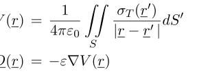
represents the dielectric slab width, and hdenotes the height between the top and bottom conductors. The solution procedure is based on the method by replacing all the conducting plates and dielectric layers with equivalent layers of unknown charge densities in free space [12]. With this replacement, the potential and electric flux density of a round disk capacitor are given by
V(r) = 1 4πε0
S
σT(r)
|r−r|dS
(1)
D(r) = −ε∇V(r) (2 )
where S is the surface of a round disk capacitor, V(r) denotes the potential by the charges, andD(r) represents the electric flux density vector. Also, σT(r) represents the total charge density composed of a free charge density lying on the plates and a bound charge density on the dielectric to dielectric interface. In here ε and ε0 are
Note that Equations (1) and (2) are represented by the free space Green’s function because the replacement of conductors and dielectrics by the equivalent surface charges has been made so that subsequent computations will be performed in a free space.
By applying the potential boundary conditions to the top and bottom plates, the potential in Equation (1) reduces to Vi for i = 1 and 2.
In order to evaluate Equation (2) along the medium interface, this equation is to be decomposed into two parts, one with the self term and the other with the mutual contribution term.
D±·(n) =Dn±(self) +D±n(P V) (3a) where
D±n(self) =
ε+σT
2ε0 for exterior region −ε−σT
2ε0 for interior region
(3b)
D±n(P V) = ε± 4πε0
P V
S
(r−r)·nˆ
|r−r|3 σT(r
)dS (3c)
In here P V (·)dS denotes the principal value of integration. The superscripts (+) and (−) represent the exterior and interior region of the medium, respectively. ˆn represents an outward normal vector directed to the exterior region. When Equation (3) is applied to a zero thickness conductor, the free charge density σf and the total charge densityσT are related as follows
∆D = (D+−D−)·nˆ
= D+n(P V)−D−n(P V) +ε
++ε−
2ε0 σT
= σf (4)
For a dielectric to dielectric boundary with no conductor present, ∆D
becomes zero since there is no free charge in this case. Once the total surface charge density σT is determined, the free charge density σf can be calculated by Equation (4). By specializing Equation (4) to a dielectric to dielectric interface, the bound charge density σb lying on that boundary is provided by
σb =
ε−−ε+ ε+ D
+·ˆn (5)
1,2,· · ·, M} is chosen, and the surface charge density is expanded in terms of the chosen expansion functions
σT = M
n=1
σT nfn(r) (6)
where fn(r) has a unit height on the nth annular patch subdomains and is zero otherwise. σT n is the expansion coefficient of the charge densities to be determined. A number M = Nc +Nd is the total number of subsections, in whichNc means the number of subdomains on the conductors, andNd represents the number on the dielectric to dielectric interface. The total M equations are required to solve σT n of which Nc equations are obtained by applying potential boundary conditions on the plates, and the remainingNdequations by applying the continuity of normal components of the electric flux density on the dielectric interface. By substituting Equation (6) into (1) and (4) on which the potentials were set to Vi and the free charge density σf set to zero, and testing of the resulting equation with each thin tube weighting function led us to obtain
Φm(fn) · · ·
∆Dm(fn)
σT n
=
V
i
· · ·
0
(7a)
where
Φm(fn) = 1 4πε0
∆Sn
dS
|rm−rn| (7b)
for m = 1,2,· · ·, Nc and n = 1,2,· · ·, M as the voltage matrix element, and
∆Dm(fn) =
(ε+−ε−) 4πε0
P V
∆Sn
(rm−rn)·nˆm
|rm−rn|3 dS+
ε++ε−
2ε0
(7c)
by using Equation (4). Hence, based on the total free chargeQand the potential difference V between the plates, the capacitance of a round capacitor can be found to be
C= Q
V =
V2−1 V1
Nct
n=1
σf n∆Sn
=
V2−1 V1
Nc
n=Nct+1
σf n∆Sn
(8)
where the superscriptt inNct denotes the top plate. In Equation (8), the third term numerator represents the total free charge on the top plate, whereas the fourth term numerator indicates the total free charge on the bottom plate due to the range of summation indexn.
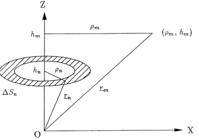
Figure 2. The coordinates for evaluating the voltage and flux matrix elements.
3. EVALUATION OF MATRIX ELEMENTS
Figure 2shows the coordinates for evaluating matrix elements in Equation (7). By taking into account the symmetry of geometry a testing point is chosen to lie on the xz plane for computational convenience purposes. In this circumstance we recognize that the distance vectorsrm and rn are
rm = ˆxρm+ ˆzhm
rn= ˆxρncosφ+ ˆyρnsinφ+ ˆzhn
(9a)
where φ is an angle between the x axis and radial distance ρn. The distance |rm−rn|from a testing point rm to source point rn is
|rm−rn|= ρ2
Substituting (9b) into Equation (7b) produces
Φm(fn) =
ρn∆Wn 2πε0
π
0
dφ ρ2
m+ρ2n+ (hm−hn)2−2ρmρncosφ = ρn∆Wn
πε0Amn
K(kmn) (10a)
where
K(x) =
π
2
0
dφ
1−x2sin2φ (10b)
A2mn = (ρm+ρn)2+ (hm−hn)2 (10c)
kmn2 = 4ρmρn
A2
mn
<1 (10d)
where ∆Wn represents the width of each annular patch with a surface ∆Sn as shown in Figure 2. In the derivation of Equation (10), a new integral variable, φ = (π − φ)/2, was introduced. K(x) in Equation (10b) is a complete elliptic integral of the first kind. With respect to nonoverlapped pulse portions (m =n), the argument x in
K(x) lies between 0 and 1, as described in Equation (10d). Hence, Equation (10) can be computed by a numerical integral technique without encountering difficulties. In regards to the coincident pulse portion (m = n), the integral is evaluated analytically. For this to occur, the nth annular subsection is divided into two parts, one of which includes a singular point and the other not. The integral contributed by a singular point will be performed over an approximate square area (∆Wn)2. In other words, by taking the angleθn= ∆Wn/ρn which yields an approximate square area around a singular point, the integral along the annular ring is separated into one ranging from −θn/2to θn/2and the other from θn/2to 2π −θn/2. After setting ρm = ρn in Equation (9b) and substituting this result into Equation (7b) shows the following equation
Φm(fn) = 1 4π ε0
∆Wn/2
−∆Wn/2
∆Wn/2
−∆Wn/2
dxdy
x2+y2 +
∆Wn 4πε0
2π−θn/2
θn/2
dφ √
2√1−cosφ
=∆Wn
πε0
ln(1 +√2 ) + ∆Wn 2πε0
In this equation, the first term is a contribution by a singular point and the second term by the remaining parts, and ln denotes the natural logarithm with a basee∼= 2.718.
Since the voltage matrix has been evaluated, the flux matrix will be computed in the next turn. The flux matrix ∆Dm(fn) in Equation (7c) has to be evaluated over the plates and the dielectric interfaces. The former is denoted by ∆Dm(fn)z and the latter by ∆Dm(fn)x, since the unit testing vector ˆnmpoints toward±ˆzdirection over the plates and ˆx direction over the dielectric interfaces when the testing point lies in the xz plane. Both ε+ and ε− will be replaced
by ε0 and ε0εr respectively, and the relation φ = (π −φ)/2will be used for computational purpose. In order to evaluate ∆Dm(fn)z for the mutual term (m =n), incorporating (rm−rn)·ˆz=hm−hn and Equation (9b) into (7c) shows
∆Dm(fn)z = (1−εr)ρn(hm−hn)∆Wn
πA3
mn
π/2
0
dφ
1−k2
mnsin2φ
3/2
= (1−εr)ρn(hm−hn)∆Wn
πA3
mn
E(kmn) 1−k2
mn
(12a)
where
E(x) = π/2
0
1−x2sin2φdφ (12b)
the functionE(x) is a complete elliptic integral of the second kind. For the self term (m=n), ∆Dm(fn)z becomes
∆Dm(fn)z = 1 +εr
2 (12c)
since the vectors rm −rn and ˆnm are orthogonal to each other in Equation (7c) for this case.
In order to calculate the flux matrix ∆Dm(fn)x for the mutual term, substituting the relation (rm −rn)·xˆ = ρm − ρncosφ and Equation (9b) into (7c) yields
∆Dm(fn)x
=1−εr 4π
∆Wn/2
−∆Wn/2
ρndρ
2π
0
ρm−ρncosφ [ρ2
m+ρ2n+(hm−hn)2−2ρmρncosφ]3/2
=(1−εr)ρn(ρm+ρn)∆Wn πA3 mn π/2 0 dφ
(1−k2
mnsin2φ)3/2
−2(1−εr)ρ2n∆Wn
πA3
mn
π/2
0
sin2φ
(1−k2
mnsin2φ)3/2
dφ
=(1−εr)ρ
2
n∆Wn
πA3
mn
1+ ρm
ρn − 2
k2
mn
E(kmn) 1−k2
mn + 2
k2
mn
K(kmn)
(13a)
In here K(x) and E(x) were already defined in Equations (10b) and (12b) respectively. For the self term, the integral is evaluated analytically. The subsection is divided into two parts; one including a singular point and the remaining parts, as done for obtaining Equation (11). Applying the similar procedure to evaluate ∆Dm(fn)x, in this case no contribution is made from a singular point since the distance vectorrm−rn is perpendicular to ˆx over this section. Thus, contributions are only made by sections excluding a singular point. Hence, the expression on ∆Dm(fn)x for the self term becomes
∆Dm(fn)x=(1−εr)ρm∆Wn 4π
2π−θn2
θn
2
ρm(1−cosφ) (√2ρm√1−cosφ)3
dφ+1 +εr 2
=(1−εr)∆Wn 4πρm
ln(cot(θn/8)) + 1 +εr
2 (13b)
By putting the matrix elements provided by Equations (10), (11), (12), and (13) into Equation (7), the charge density coefficient σT n can now be determined. Once the total charge density distributions by using Equation (7) are determined, the electric potentialV(r) at the field point r can be computed by superposing potential contributions in terms of segment charges residing on the annular patches, which is written as
V(r) = M
n=1
φa(r :rn) (14)
inversion on Equation (7). By using Equation (14), the equipotential lines can be drawn around the round disk capacitor as depicted in Figure 6.
4. NUMERICAL EXAMPLES
To illustrate the validity and usefulness of our numerical scheme, this method was applied to a single circular disk with radius a which was charged to a constant potential V0. The accurate charge density
distribution on this disk is given by [13, 14]
σ(ρ) = 4V0ε0
π a2−ρ2 (15)
where ρ is the distance from the center of a disk. The capacitance of this disk is 8ε0a, which is also an exact solution. For a numerical
solution, the disk was divided into M equidistant annular patch subsections, in which the constant charge density distribution on each subsection was assumed.
Computation has been conducted for a single circular disk with radius a = 1 and voltage V0 = 1[V] by using the number of annular
patch M as 30. Figure 3 illustrates an excellent match between the exact and computed charge density distribution for the circular disk.
Figure 3. Charge density distribution of a single circular disk (a= 1,
V0 = 1[V]).
capacitance of a single circular disk with respect to the number of employed subsections is presented for comparison between the annular and triangular subsections [15]. The data in Table 1 represents the normalized capacitance of C/a, with respect to the disk radius a. The relative errors are less than 1% for a matrix size of 20 and of 0.5% for 40, respectively. As shown in this table, results by annular patch subsections show much smaller errors than those of triangular patches with the same matrix size. The computed solution is becoming convergent to the exact solution by increasing the number of annular subsections.
Table 1. Normalized capacitance of a single circular disk [pF/m].
Annular patch Triangular patch [15]
M C/a % error M C/a % error 10 69.57 1.76 18 59.80 15.57 15 70.01 1.16 30 61.10 13.74
20 70.22 0.86 42 61.80 12.75 25 70.35 0.68 54 62.24 12.13 30 70.43 0.56 60 66.03 6.78
40 70.55 0.41 84 66.72 5.72
exact 70.83
The round disk capacitor under consideration was shown in Figure 1. Figure 4 shows the computed charge distribution of a round disk capacitor for W = 0 in Figure 1; The protruded dielectric slab is just fitted in between the upper and lower conducting plates. In this figure, both radius a and height h were set to be unity, and the voltages to be V1 =−V2 = 1[V]. In other words, +1[V] is applied to
the top plate and−1[V] to the bottom plate so that 2[V] is maintained between the plates. Thus the 0[V] equipotential line is formed along the center line. Figure 4 shows a parallel-plate capacitor filled with a relative dielectric constant of εr = 3.0. The portions between node A and B are the metals together with the opposite side, and the portions between node B and D are the dielectric layers.
and bound charges. However, the total charge on the dielectric layer is just a bound charge in itself. This bound charge density is marked with a dotted line in Figure 4, together with its sign as determined by the portions of where it belonged. The sign of a bound charge is negative on portions A and B, but it becomes positive on portions B and C since the bound charges are the induced polarization charge in character. A solid line indicates the total charge density. Its value is lower than that of a free charge on portions A and B because it is a sum of positive free charge and negative bound charges. It is noted that the singular behavior around the corners is observed, as seen in Figure 3.
The ratio between the amount of the total charge to the free charge was about 2.2 at the center of the node between A and B, as shown in Figure 4. Along the node boundary between A and B, the positive free charge density and negative bound charge density due to the induced polarization charges appeared as expected, since the potential of the upper plate is higher than the lower plate. The discontinuity of a bound charge at the corner of a capacitor, marked B and D in Figure 4, is due to the singular behavior of the electric field at these locations. The direction of the electric field lines emanating from the top to bottom plate over layer B-C-D dictates the sign of the bound charge along this boundary. Actually, the fringing (or leakage) electric field starts at B, passes through C, and ends at D. The point C is located at the right hand side of point C. The bound charges lying along nodes B-C-D are responsible for the fringing field effect. They cause bending
of the equipotential lines across the dielectric interfaces. However, for a small h/a ratio, the ratio of total to free charge is nearly unity and eventually the fringing field has little significance. In other words, the distance between point C and C becomes smaller as the ratio of h/a
is decreasing, eventually the range of electric field leakage extending to the outside of the capacitor is diminished.
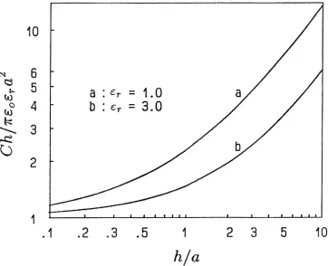
Figure 5. Normalized capacitance vs parameter h/a.
Figure 5 represents the capacitance of a round disk capacitor as a function of normalizedh/a forεr = 1.0 and 3.0, respectively. In the light of Equation (16), the normalization is scaled toh/a for abscissa andCh/πε0εra2 for ordinate. Under the adopted normalization scale, Figure 5 illustrates the expected behavior. It is noticed that the logarithmic scale has been used to both axes.
Figure 6 shows the equipotential lines on thexz plane. The lines are nearly parallel to each other in the interior region, but somewhat bent at the corner due to the fringing field effect. At the corner, the lines forεr= 3.0 are more parallel in comparison to those forεr = 1.0. This is due to the fact that the fringing field becomes smaller asεr is increasing. However, the equipotential lines forεr = 3.0 exhibits sharp bending at the boundary (x= 1) because the normal component of the electric field over the layer is discontinuous at a dielectric to dielectric interface due to the existing bound charges. The equipotential lines as seen in Figure 6 reflect these features. All of the electric field lines, though not shown, would be perpendicular to the equipotential lines shown in Figure 6.
Figure 6. Equipotential lines of a round disk capacitor.
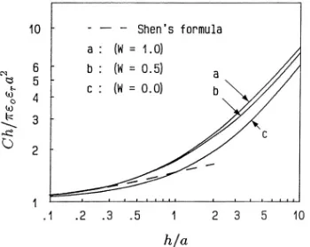
Figure 7. Normalized capacitance versus parameterh/a for a round disk capacitor with a partially filled dielectric slab (εr= 3.0).
these values together with results obtained by Shen’s formula [4]
C =εr
ε0πa2 h
1 + 2h
πεra
ln
πa
2h
+ 1.7726
(16)
derivation. In this figure, as the uncovered dielectric slab width
W is increasing with respect to the length of conducting plate, the corresponding capacitance is slightly increased, thereby the fringing field effect becomes somewhat more evident. Due to the involvement of the fringing field, the discrepancies between the numerical solutions (indicated by a solid line) and Shen’s results (indicated by a broken line) are proportionally increasing as the amount of ratioh/ais being increased. The smallest error which occurred was at theh/a= 0.1 in Figure 7, as expected.
5. CONCLUSION
A solution procedure to analyze a round disk capacitor was introduced by using annular patch subdomains. Based on this technique, the discretizing errors on the capacitor surfaces could be completely removed, which made it possible to achieve more accurate numerical results together with savings on computation time as well as memory. These benefits were possible due to the perfect match between the shape of the round disk and the employed annular patches. For numerical calculation, pulses on the annular patches were taken as the expansion functions and zero thickness thin tubes were chosen as the testing functions, which eventually led to the point matching.
To show the effectiveness on the proposed scheme, this technique was applied to a single circular disk and to a capacitor filled with a dielectric slab covered by partial plates. The calculated capacitances for these structures showed good agreement with known solutions. The total charge density, free charge density, and bound charge density along the capacitor boundary were calculated and sketched to provide understanding on the leakage field. By drawing the equipotential lines around the capacitor, discussions were also made on the resultant fringing field effects related to the bound charge densities lying on the dielectric interfaces.
ACKNOWLEDGMENT
This paper is dedicated to the memory of Professor Jin Au Kong.
REFERENCES
2. Benedex, P. and P. Silvester, “Capacitance of parallel rectangular plates separated by a dielectric sheet,” IEEE Trans. Microwave Theory Tech., Vol. 20, 504–510, Aug. 1972.
3. Itoh, T. and R. Mittra, “A new method for calculating the capacitance of a circular disk for microwave integrated circuit,” IEEE Trans. Microwave Theory Tech., Vol. 21, 431–432, 1973. 4. Shen, L. C., S. A. Long, M. R. Allerding, and M. D. Walton,
“Resonator frequency of a circular disk, printed circuit antenna,” IEEE Trans. Antennas Propagat., Vol. 25, 595–596, July 1977. 5. Pyati, V. P., “Capacitance of a circular disk placed over a
grounded substrate,” Journal of Electromagnetic Waves and Applications, Vol. 1, No. 11, 1013–1025, 1997.
6. Jiang, L. J. and W. C. Chew, “A complete variational method for capacitance extractions,” Progress In Electromagnetics Research, PIER 56, 19–32, 2006.
7. Harrington, R. F.,Field Computation by Moment Methods, 24–28, N.Y. Macmillan Co., 1968.
8. Ghosh, S. and A. Chakrabarty, “Capacitance evaluation of arbitrary-shaped multiconducting bodies using rectangular subareas,” Journal of Electromagnetic Waves and Applications, Vol. 20, No. 14, 2091–2102, 2006.
9. Reitan, D. K., “Accurate determination of the capacitance of rectangular parallel-plate capacitor,”Journ. Appl. Phys., Vol. 30, No. 2, 172–176, Feb. 1959.
10. Harrington, R. F., “Matrix methods for field problems,” Proc. IEEE, Vol. 55, No. 2, 136–149, Feb. 1967.
11. Wei, C. W., R. F. Harrington, J. R. Mautz, and T. K. Sarkar, “Multiconductor transmission lines in multilayered dielectric media,” IEEE MTT, Vol. 32, No. 4, 439–450, Apr. 1984.
12. Stratton, J. A.,Electromagnetic Theory, 183–185, N.Y. McGraw-Hill, 1941.
13. Griffiths, D. J. and Y. Li, “Charge density on a conducting needle,” Am. J. Phys., Vol. 64, No. 6, 706–714, June 1996. 14. Liang, C. H., H. B. Yuan, and K. B. Tan, “Method
for largest extended circle for the capacitance of arbitrarily shaped conducting plates,”Progress In Electromagnetics Research Letters, Vol. 1, 51–60, 2008.
![Figure 3. Charge density distribution of a single circular disk (a = 1,V0 = 1[V ]).](https://thumb-us.123doks.com/thumbv2/123dok_us/1905072.1249531/10.612.168.351.383.552/figure-charge-density-distribution-single-circular-disk-v.webp)
![Table 1. Normalized capacitance of a single circular disk [pF/m].](https://thumb-us.123doks.com/thumbv2/123dok_us/1905072.1249531/11.612.157.366.254.377/table-normalized-capacitance-single-circular-disk-pf-m.webp)