Technique into Software on Multicore
Zhimin Chen and Patrick Schaumont
ECE Department, Virginia Tech Blacksburg VA 24061, USA {chenzm, schaum}@vt.edu
Abstract. This paper discusses a novel direction for multicore crypto-graphic software, namely the use of multicore to protect a design against side-channel attacks. We present a technique which is based on the princi-ple of dual-rail pre-charge, but which can be comprinci-pletely imprinci-plemented in software. The resulting protected software is called a Virtual Secure Cir-cuit (VSC). Similar to the dual-rail pre-charge technique, a VSC executes as two complementary programs on two identical processor cores. Our key contributions include (1) the analysis of the security properties of a VSC, (2) the construction of a VSC AES prototype on a dual-PowerPC ar-chitecture, (3) the demonstration of VSC’s protection effectiveness with real side-channel attack experiments. The attack results showed that the VSC protected AES needs 80 times more measurements than the unpro-tected AES to find the first correct key byte. Even one million measure-ments were not sufficient to fully break VSC protected AES, while un-protected AES was broken using only 40000 measurements. We conclude that VSC can provide a similar side-channel resistance as WDDL, the ded-icated hardware equivalent of dual-rail pre-charge. However, in contrast to WDDL, VSC is a software technique, and therefore it is flexible.
1
Introduction
Improving the performance and the security of cryptographic software has al-ways been an important research topic, in particular because of the broad us-age of software cryptography. In recent years, as the underlying computing platform switches from single-core to multi-core processors, cryptographic en-gineers face new challenges. While we see a lot of effort on parallel implemen-tations of cryptography for better performance, we have not started to explore the potential of multicore for better security. In this paper, we focus on the secu-rity issues and present our work on protecting cryptographic software against power-based Side-Channel Attacks (SCA) [1] on multi-core platforms.
randomization is the higher-order attack [8], which exploits the side-channel leakage by jointly observing multiple intermediate values in the cryptographic device [9]. A higher-order attack can be thwarted using higher-order random-ization [10], but the complexity of such higher-order randomrandom-ization techniques increase exponentially with the order number [11].
Besides randomization, hiding is another popular SCA countermeasure. It protects the cryptographic devices by reducing the signal-to-noise ratio of the side-channel leakage. In hardware, hiding can be implemented using Dual-Rail Pre-charge (DRP) circuits [12]. By implementing a true and a complementary form for each logic function in the cryptography, DRP circuits exhibit constant power-consumption, which thwarts SCA.
In contrast to randomization techniques, so far the DRP technique hasn’t been used in software countermeasures. The reason is that it needs simultane-ous execution of true and complementary logic functions, which cannot be real-ized in single-core processors. However, as multi-core platforms are becoming ubiquitous in PCs and embedded systems, implementing the DRP technique in software becomes a viable solution. In this paper, we propose a design method that can protect cryptographic software with the DRP technique. We will show that our method creates the software equivalent of a DRP secure circuit, and hence we call the protected software a Virtual Secure Circuit (VSC).
The key contributions of this paper are as follows. First, we perform se-curity analysis on VSC and explain why a software-based DRP technique can withstand side-channel power attacks. Second, we construct a VSC proteced AES prototype on a dual-PowerPC computing platform.Third, we successfully demonstrate VSC’s protection effectiveness by means of a set of real power based side-channel attacks on the prototype. Attack results show that VSC of-fers a considerable improvement on the security by increasing the Measure-ments To Disclosure (MTD) at least 80 times. Even 1 million traces are not suf-ficient for a successful full attack.
2
Dual-Rail Pre-charge (DRP) Technique
Power-based side-channel attacks obtain secret information from a cryptographic device by observing data-dependent variations in the power dissipation. The DRP technique aims to make the power dissipation constant so that no infor-mation is leaked. This is achieved by combining two techniques: 1) dual-rail (complementary) logic and 2) dynamic logic. The first of these makes the static power dissipation of a constant. The combination of both also makes the dy-namic power dissipation constant. So far, the DRP technique has only been used in hardware, for example in SABL [12], in WDDL [13], and in MDPL [14].
A
B Q
Static Power Dynamic Power
1 1 0 1 0 1 1
AP
BP QP
0 AP
BP
QP A
B
Q
AP
BP
1 0 1 0 1 0 1 AP
BP
QP QP
(a) (b)
Standard NAND gate
WDDL NAND gate
1 1 1 1 1 1 1 Static Power
Dynamic Power
Fig. 1. (a) A CMOS standard NAND has data-dependent power dissipation; (b) A WDDL NAND gate has a data-independent power dissipation.
static power is 0, both inputs must be 1. This side-channel leakage is the basis for SCA.
Fig. 1b shows the same test case on a WDDL NAND gate. In this case, the circuit encodes each logic value with a complementary pair(Ap, Ap). Further-more, each pair is pre-charged to (0,0) in each clock cycle before evaluation. As a result, each clock cycle, every WDDL signal pair shows exactly one transition from 0 to 1 and another one from 1 to 0. The resulting static and dynamic power dissipation are now independent of the input values of the WDDL gate.
Despite the elegance of this concept, DRP circuits in hardware do have some disadvantages. First, DRP circuits are at least two times larger than equivalent standard CMOS circuits, and they have a much larger power dissipation. Sec-ond, the constant-power argument, based on Hamming Weight or Hamming Distance, does not hold when low-level electrical effects are taken into account. Small asymmetries between the true and complementary paths of a signal pair still may lead to residual side-channel leakage. Nevertheless, hardware DRP circuits are able to increase the number of measurements for a successful SCA to a prohibitive amount [15].
3
Virtual Secure Circuit (VSC)
In this section, we introduce the Virtual Secure Circuit (VSC), the software equivalent of DRP circuits in hardware. We first clarify a few initial assump-tions on the hardware. Next, we describe a multicore architecture that serves as the target for VSC, and we present the design of a VSC by means of an exam-ple. Finally, we show that a VSC is functionally equivalent to a DRP circuit in hardware, with similar security properties.
3.1 Micro-Processor Assumptions and Side-channel Leakage
ALU Reg. File
MUX
MUX
imm.
A
C B
Memory
Memory interface datapath 1
datapath 2
datapath 3
(a) (b)
A
C B
Fig. 2.Processor architecture: (a) Three datapaths in a processor [18]; (b) Datapath for ANDoperation.
we make the following assumptions regarding their implementation. First, we assume that we can build the multi-core platform from small microprocessors or micro-controllers, which have a well-defined instruction-execution pattern. For example, we assume deterministic memory-access time (no cache), and we assume there are no state-dependent processor features (no branch predictors). Second, we assume that VSC can run as an atomic thread of control on the multicore architecture. Thus, we assume that interrupts and exceptions can be disabled for the duration of the complementary program execution. These two assumptions ensure that it is feasible to maintain synchronization between the cores. These assumptions do not mean that VSC will never be able to support more complex architectures. In this paper, as the first step, we only focus on the simple case. Even in its simplest form, we can still point out practical imple-mentation scenarios for VSC. For example, tiled processors [16], an important category of multicore processors, are usually built with small processing cores and local memories. The local memories for 8 Synergistic Processing Elements (SPE) in the Cell processor [17] are not cache either.
Given the above assumptions, we now analyze what parts of the micro-processor are potential sources of side-channel leakage. For this purpose, we analyze the flow of information within a microprocessor, as shown in Fig. 2a. We can distinguish three different datapaths. The first datapath is the compu-tational datapath. It starts from the register file, goes through the Arithmetic Logic Unit (ALU), and returns to the register file. For memory-operations, there are two additional datapaths. The memory-load datapath is used to transfer in-formation from memory to the register file. The memory-store datapath is used to transfer information from the register file to the memory.
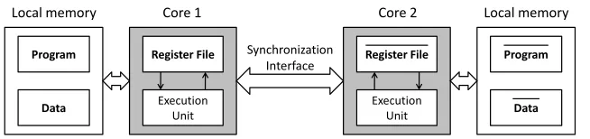
Program
Data
Register File
Execution Unit
Program
Data Register File
Execution Unit
Core 1 Core 2
Local memory Local memory
Synchronization Interface
Fig. 3.A system architecture to implement a Virtual Secure Circuit.
3.2 Multi-core Architecture for VSC
Fig. 3 illustrates the system architecture used for a VSC. In a multi-core archi-tecture, two structurally identical cores are selected. Both cores execute com-plementary versions of the same program: core 1 executesP rogram, while core 2 executes P rogram. The rules for creating the instructions ofP rogram and
P rogramfollow the principles of the DRP technique. For each instruction in
P rogram, there is a complementary instruction inP rogram. Acomplementary instructionpair maps complementary input data into complementary output data. Section 5 will describe such instruction pairs in more detail.
During the execution of these complementary programs, both cores main-tain cycle-accurate synchronization, which is achieved by means of a synchro-nization interface. This ensures that both cores execute complementary instruc-tion pairs in the same clock cycle. As a result of executing complementary instructions, both cores also handle complementary data stored in their reg-ister file as well as in their local memory. To extend the DRP technique into storage, the register file and the local memory are both pre-charged whenever new data is stored. In this way, any data-dependent power consumption in core 1 is matched by a complementary data-dependent power consumption in core 2, so that the overall power consumption of the multi-core system is data-independent.
To implement the above concept, we need 1) to convert the ordinary soft-ware into the complementaryP rogramandP rogram, and 2) to design a dual-core system where two dual-cores can be synchronized with clock-cycle accuracy. In this section, we only discuss the program conversion while including processor synchronization to the Appendix.
3.3 CreatingP rogramandP rogram
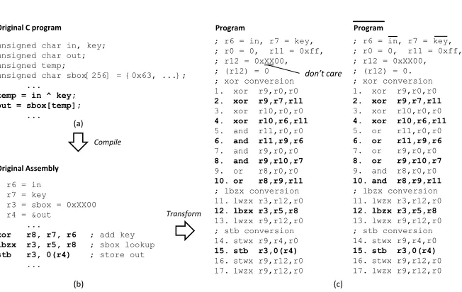
A case study is used to explain how the program conversion looks like. Fig. 4 shows the conversion of part of the AES encryption round. In Fig. 4a, the AES
AddRoundKeyandSubByteoperations are implemented with two lines of C
; r6 = in ; r7 = key
; r3 = sbox = 0xXX00 ; r4 = &out
...
xor r8, r7, r6 ; add key lbzx r3, r5, r8 ; sbox lookup stb r3, 0(r4) ; store out
...
; r6 = in, r7 = key, ; r0 = 0, r11 = 0xff, ; r12 = 0xXX00, ; (r12) = 0 ; xor conversion
1. xor r9,r0,r0
2. xor r9,r7,r11 3. xor r10,r0,r0 4. xor r10,r6,r11 5. and r11,r0,r0 6. and r11,r9,r6 7. and r9,r0,r0 8. and r9,r10,r7 9. or r8,r0,r0 10. or r8,r9,r11 ; lbzx conversion 11. lwzx r3,r12,r0 12. lbzx r3,r5,r8 13. lwzx r9,r12,r0 ; stb conversion 14. stwx r9,r4,r0 15. stb r3,0(r4) 16. stwx r9,r12,r0 17. lwzx r9,r12,r0
Program Program
Original C program
Transform Compile
; r6 = in, r7 = key, ; r0 = 0, r11 = 0xff, ; r12 = 0xXX00, ; (r12) = 0. ; xor conversion 1. xor r9,r0,r0 2. xor r9,r7,r11 3. xor r10,r0,r0 4. xor r10,r6,r11 5. or r11,r0,r0 6. or r11,r9,r6 7. or r9,r0,r0 8. or r9,r10,r7 9. and r8,r0,r0 10. and r8,r9,r11 ; lbzx conversion 11. lwzx r3,r12,r0 12. lbzx r3,r5,r8 13. lwzx r9,r12,r0 ; stb conversion 14. stwx r9,r4,r0 15. stb r3,0(r4) 16. stwx r9,r12,r0 17. lwzx r9,r12,r0 unsigned char in, key;
unsigned char out; unsigned temp;
unsigned char sbox[256] = {0x63, ...}; ...
temp = in ^ key; out = sbox[temp];
...
Original Assembly
(a)
(b) (c)
don’t care
Fig. 4.An example of Virtual Secure Circuit: (a)KeyAdditionandSubByteoperations in C code; (b) Compiled assembly code; (c) Converted VSC assembly code.
two steps. The first step is to create complementary instruction pairs. The sec-ond step is to integrate the pre-charge operations.
Step 1: Complementary instruction pairs are shown in bold typeface in
Fig. 4c. We first consider the conversion of thexoroperation. Its complemen-tary instruction,xnor, is unavailable on the PowerPC instruction set used here. Therefore the original logic functionr8 = r7⊕r6is expanded intor8 = r7·
r6 +r6·r7 inP rogram and intor8 = (r7 +r6)·(r6 +r7)in P rogram. In Fig. 4c, the converted code uses 5 steps to complete the new equations with the help of 3 temporary registersr9,r10, andr11. The remainingxoroperations, on line 2 and line 4, are used to invert the lowest byte and do not violate the complementary rule. Finally, since the memory-load (lbzx) and memory-store (stb) instructions do not change their operands’ value, their complementary instructions are themselves.
Step 2:The instructions in regular typeface in Fig. 4c are used for pre-charge. They do not affect the computation results. Instead, they reset the execution circuits and storage, between the computational instructions. Most instructions in Fig. 4c (namely, those in the computational datapath) use a single pre-charge instruction. Memory-load and Memory-store instructions may need more than a single pre-charge instruction, depending on the presence of sensitive data in the address or data of the memory-access operation. Section 5 will discuss these in more detail.
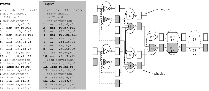
2 2 4 4 6 8 6 8 LUT LUT
; r0 = 0, r11 = 0xff, ; r12 = 0xXX00, ; (r12) = 0 ; xor conversion 1. or r9,r0,r0
2. xor r9,r7,r11
3. or r10,r0,r0
4. xor r10,r6,r11
5. and r11,r0,r0
6. and r11,r9,r6
7. and r9,r0,r0
8. and r9,r10,r7
9. or r8,r0,r0
10. or r8,r9,r11
; lbzx conversion 11. lwzx r3,r12,r0
12. lbzx r3,r5,r8
13. lwzx r9,r12,r0 ; stb conversion 14. stwx r9,r4,r0
15. stb r3,0(r4)
16. stwx r9,r12,r0 17. lwzx r9,r12,r0
Program Program
; r0 = 0, r11 = 0xff, ; r12 = 0xXX00, ; (r12) = 0. ; xor conversion 1. or r9,r0,r0
2. xor r9,r7,r11
3. or r10,r0,r0
4. xor r10,r6,r11
5. or r11,r0,r0
6. or r11,r9,r6
7. or r9,r0,r0
8. or r9,r10,r7
9. and r8,r0,r0
10. and r8,r9,r11
; lbzx conversion 11. lwzx r3,r12,r0
12. lbzx r3,r5,r8
13. lwzx r9,r12,r0 ; stb conversion 14. stwx r9,r4,r0
15. stb r3,0(r4)
16. stwx r9,r12,r0 17. lwzx r9,r12,r0
10 10 12 12 15 15 regular shaded
Fig. 5.Mapping from software dataflow to secure circuit: by instantiating the each pro-cessor’s active datapath at different time, we obtain a DRP secure circuit.
3.4 A VSC Is Equivalent to A DRP Circuit
Finally, we demonstrate that a VSC is functionally equal to a DRP circuit. Fig. 5 shows the example of the previous section, together with an equivalent DRP circuit. Each active (bold) instruction ofP rogramorP rogramcorresponds to a single logic gate (or function) in the circuit. The numbers annotated within the logic gates correspond to line numbers in the programs. In between each logic gate, a register is inserted. The pre-charge operation will reset that register be-fore loading it with sensitive data.P rogramandP rogramexecute in lockstep, and for each tuple of instructions, exactly two complementary gates of the cir-cuit will evaluate. Hence, we conclude that a VSC is a sequentialized version of a DRP. Therefore, the VSC may inherit the properties of a DRP. In the next section, we describe a prototype implementation of AES as a VSC, followed by real side-channel attacks.
4
VSC AES Prototype Resists SCA
In the previous section we introduced the concept of a VSC. In this section we construct a VSC AES prototype and demonstrate that VSC works in reality.
4.1 VSC AES Prototype
AES under test uses a 128-bit key (16 key bytes from key[0] to key[15]). We first implemented two version of AES: regular AES, and VSC AES, represented
byAESand VSC-AESrespectively. The implementation ofAESwas based on
the standard AES algorithm description [19]. Based on that, we convertedAES
toVSC-AESby using the DRP technique to protect the 3 datapaths in the Pow-erPC processors. Some conversion technical details will be discussed in Section 5.
4.2 Side Channel Analysis Setup
We also built a SCA attack system, in which a computer was able to automati-cally send random plaintexts to the FPGA, start the encryption, control the os-cilloscope to sample current traces, and finally obtain the traces from the oscil-loscope. The current flowing through the FPGA is measured as the side-channel information. During each power attack, the AES key remained unchanged. The
KeyGenerationprocess only ran once. So our attack focused on the regular
encryption operations.
Correlation Power Attacks (CPA) [20] were mounted on theSubByte’s out-put in the first AES round. Since the attackers could not figure out the exact time when the sensitive data would appear before the analysis, the oscilloscope sampled the current trace of the entire first round. Moreover, to save the space of waveform and shorten the analysis time, the oscilloscope worked in the ‘av-erage’ mode. Every current trace the computer obtained was the average of 32 normal traces (with the same plaintext). Hamming weight of the sensitive data is used as the power model. Because of the pre-charge process, this power model is the best forVSC-AES. Hamming distance may work better forAES, but this requires the attackers to get access of the software, which cannot always be fullfiled. Therefore, Hamming weight is also chosen forAES. The improvement
ofVSC-AESoverAESobtained based on this power model is a conservative
one.
4.3 Results
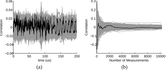
Fig. 6 shows an example of the attack results on one ofAES’s key bytes (key[3]). With only 256 measurements, we were able to find the first correctly attacked key byte ofAES. When the number of measurements increased to 40960, all the 16 key bytes were revealed.
0 50 100 150 200 −0.1
−0.05 0 0.05 0.1
Time (us)
Correlation
(a)
0 2000 4000 6000 8000 10000 −0.2
−0.1 0 0.1 0.2 0.3
Number of Measurements
Correlation
(b)
Fig. 6.Attack result on unprotected AES: (a) Correlation between the sampled current and the power estimations with 10240 measurements; (b) Correlation between the sam-ple current and the power estimations at the point where the attacked key is identified. Correct key’s trace is plotted in black, while all other key’s traces are in gray. The emerged black trace means successful attack.
0 50 100 150 200
−0.06 −0.04 −0.02 0 0.02 0.04 0.06
time (us)
Correlation
(a)
0 2000 4000 6000 8000 10000 −0.2
−0.1 0 0.1 0.2 0.3
Number of Measurements
Correlation
(b)
Fig. 7.Attack result on protected VSC-AES: (a) Correlation between the sampled current and the power estimations with 10240 measurements; (b) Correlation between the sam-ple current and the power estimations at the point where the attacked key is identified. Correct key’s trace is plotted in black, while all other key’s traces are in gray. The buried black trace means unsuccessful attack.
20480 measurements. Further, even with 1024000 measurements, 3 key bytes were still unattackable.
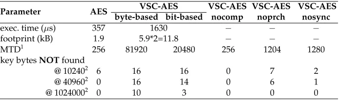
It is clear that, compared withAES,VSC-AEShas obvious reduction of side-channel leakage. We use the number of measurements to disclosure (MTD) to quantify the resistance against power attacks. Disclosure here means that at least one key byte is broken. Based on thebyte-basedHamming weight model,
VSC-AES’s improvement on MTD overAESis 320 times. Based on thebit-based
Table 1.Attack results summary.
Parameter AES VSC-AES VSC-AES nocomp
VSC-AES noprch
VSC-AES nosync byte-based bit-based
exec. time (µs) 357 1630 − − −
footprint (kB) 1.9 5.9*2=11.8 − − −
MTD1 256 81920 20480 256 1204 1280
key bytesNOTfound
@ 102402 6 16 16 0 7 2
@ 409602 0 16 14 0 6 1
@ 10240002 0 10 3 0 0 0
1
To find the first uncovered key byte.
2
Number of measurements.
To further verify the correctness of VSC, we mounted attacks on variants of VSC-AES: 1) only the true path ofVSC-AESwithout the complementary path (VSC-AESnocomp), 2)VSC-AESwith the true path 1 clock cycle ahead of the complementary path (VSC-AESnosync), and 3)VSC-AESwithout pre-charge operations (VSC-AESnoprch). All these designs could be broken much more easily thanVSC-AESas shown in Table 1.
Table 1 summarizes the results of the above attacks. VSC-AES pays 4.57 times of execution time and 6.21 times of footprint for a much higher capa-bility of resisting power attacks. Also, complementary operations, pre-charge, and synchronization are demonstrated to be three indispensable conditions for protection.
In summary, though the experiments, VSC showed its effectiveness on pro-tecting AES software. The side-channel resistance ofVSC-AESis comparable to the resistance offered by the WDDL prototype IC chip [15]. Compared with the unprotected designs, their improvements in terms of MTD are both around 100. With 1 million measurements, both can prevent a full discovery of the en-tire AES key.
5
Implementation Details on VSC-AES
This section lists some detailed design issues ofVSC-AESto share our experi-ences on the VSC programming techniques.
We first define two terms: ‘sensitive data’ and ‘related data’.Sensitive datais the intermediate data of the software that is generated with the cryptographic key, both directly and indirectly.Related datais the intermediate data that is not sensitive but will affect somesensitive data. Obviously,sensitive datais what we have to protect. Sincerelated datawill affect thesensitive data, during the VSC conversion, we also have to convert them into complementary format.
logic instruction shift instruction
and r1,r2,r3 slwi r1,r2,imm (imm<=16)
Program Program Program Program
li r0,0
and r1,r0,r0 and r1,r2,r3
li r0,0 or r1,r0,r0 or r1,r2,r3
li r9,0 slwi r11,r9,imm slwi r11,r2,imm li r10,0 xor r1,r9,r9 xor r1,r11,r10
li r9,0 slwi r1,r9,imm slwi r1,r2,imm li r10,2imm-1 xor r1,r9,r9 xor r1,r11,r10
data instructions
stb r1,imm(r2) lbzx r1,r2,r3 (access SBox)
Program Program Program Program
; (r12) = 0 ; r0 = 0 li r9,0 stw r9,imm(r2) stb r1,imm(r2) stwx r9,r12,r0 lwzx r9,r12,r0
; (r12) = 0 ; r0 = 0 li r9,0 stw r9,imm(r2) stb r1,imm(r2) stwx r9,r12,r0 lwzx r9,r12,r0
; (r12) = 0 ; r12 = 0xXX00 ; r2 = 0xXX00 ; r0 = 0 li r9,0 lwzx r1,r12,r0 lbzx r1,r2,r3 lwzx r9,r12,r0
; (r12) = 0 ; r12 = 0xXX00 ; r2 = 0xXX00 ; r0 = 0 li r9,0 lwzx r1,r12,r0 lbzx r1,r2,r3 lwzx r9,r12,r0
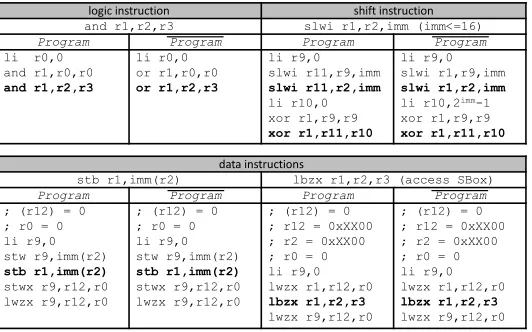
Fig. 8.Representative conversion examples.
data instructions, such asmove,loadandstore; Different categories operate differently in the processor. Accordingly, different conversion rules are needed.
Logic Instructions. Logic instructions are easy to complement. For example,
andandorare complementary.notcomplements itself. If a logic instruction has no complement in the instruction set (such asxor), we can decompose it into simpler logic operations and complement those. The rules for pre-charge are easy as well, and simply evaluate all-0 inputs for the pre-charged instruc-tions. Figure 8 shows an example.
Shift Instructions. Shift operations are usually implemented with several shift levels of combinational multiplex logic. They are basically data movement op-erations. So the complementary instruction are themselves. The same as logic instructions, shift instructions are also implemented in ALU. So the pre-charge method is the same as logic instructions. Besides that, special attention should be paid to therelated datagenerated by shift operations. A shift or rotate instruc-tion may shift the non-sensitive bits into dataflow, for example inserting 0 to the vacant bits. If these vacant bits are used to calculate thesensitive data, they be-comerelated data. Therefore, these bits need to be 1 inP rogram. After the shift instruction, we need to invert the shifted-inrelated datainP rogramwhile keep them as they were inP rogram. Fig. 8 shows a representative example.
Data Instructions. Data instructions do not change the value of the data, so
There are two scenarios. First, only the data bus carriessensitive data. Sec-ond, a special case happens when the processor tries to read an element from the SBox in theSubBytestep. During this process, not only the data buses carry the sensitiveSubByteresult, the address buses are also sensitive since it is re-lated to theAddRoundKey’s result. While the first case can easily be handled, special efforts are needed for the second case. To make sure the data buses carry complementary data, in P rogram, complementary SBox elements should be stored in the complementary addresses. We define the SBox in the ordinary pro-gram,P rogramandP rogramasSBox,SBoxcandSBoxc respectively. Their relationship should be :SBox(i) =SBoxc(i) =bitnot(SBoxc(bitnot(i))). More-over, the address buses should also be complementary. A possible problem is as follows. Suppose the SBoxc and SBoxc’s base addresses are both 0x0001. WhenP rogramloadsSBoxc(0),P rogramloadsSBoxc(255). The actual value on the address bus is the sum of the base address and the element’s index, namely the offset address. In the above case, the values on the address buses are 0x0001 and 0x0100, which is obviously not complementary. Our solution is to align bothSBoxcandSBoxcto the28-byte boudary (SBox’s base address is 0xXX00. XX means ‘do not care’ and can be different forSBoxcandSBoxc). In this case, the values on the address buses of two cores are 0xXX00 and 0xXXFF. The sensitive part of the address buses are complementary.
We reserve a word which stores 0 in the memory. The 0 value is used to pre-charge the data buses. When the address buses contain sensitive data, the address of the reserved word should also be aligned to the28-byte boudary (e.g. r12=0xXX00 in Fig. 4). When accessing this reserved address, the lowest byte of the address bus is pre-charged to all 0. With the above preparation, the pre-charge operations reset the memory bus and the storage in the way shown in Fig. 8. Finally, if the value in the source register or memory is not used later, we reset it to 0.
With the above techniques, we were able to convert the full AES software into VSC protected AES.
6
Discussion
Due to the special requirement on perfect synchronization between two cores, we expect that the embedded multicore system can work in two modes: ‘normal mode’ and ‘secure mode’, which borrows the idea from the ARM Trust-Zone [21]. In the ‘secure mode’ for VSC, cache, interrupts, and exceptions are all disabled. The related work is one of our research topics in the future.
7
Previous Works
A previous similar work, called MUTE-AES, was presented in 2008 [22]. Both VSC and MUTE-AES follow the idea of running the direct and complementary copies of a cryptographic algorithm on two identical cores to generate data-independent power. Despite their similarity, there are significant differences between our work and the previous work.
– VSC and MUTE-AES are at different level of abstraction. VSC deals with the processor instructions, while MUTE-AES is based on modifying AES algorithm. As a result, VSC is a general protection solution, like WDDL, while MUTE-AES only applies to AES algorithm.
– Unlike VSC, MUTE-AES does not strictly follow the principles of the DRP technique. There is no pre-charge operations in MUTE-AES. Based on our experimental results in Table 1, without pre-charge (VSC-AESnoprch), the crypto-system can still be easily attacked.
– We not only show VSC’s improvement qualitatively but also quantify the improvement with real Side Channel Attacks. For MUTE-AES, the exper-iment was based on simulation and the improvement was not quantified. Hence, there is no way to see how much better security that MUTE-AES can supply.
– The method to perfectly synchronize two cores for MUTE-AES is to rec-ognize the program pattern of the AES software’s assembly codes. This method is potentially false positive, not to mention it is specific to a sin-gle program. In contrast, as shown in the Appendix, VSC’s synchroniza-tion method is simpler and more generic and is not false-positive nor true-negative.
8
Conclusion
References
1. Kocher, P.C., Jaffe, J., Jun, B.: Differential Power Analysis. CRYPTO 1999, LNCS1666
(1999) pp. 388–397
2. Herbst, C., Oswald, E., Mangard, S.: An AES Smart Card Implementation Resistant to Power Analysis Attacks. ACNS 2006, LNCS3989(2006) pp. 239–252
3. Oswald, E., Schramm, K.: An Efficient Masking Scheme for AES software Imple-mentations. WISA 2005, LNCS3786(2005) pp. 292–305
4. Coron, J., I, K.: An Efficient Method for Random Delay Generation in Embedded Software. CHES 2009, LNCS5747(2009) pp. 156–170
5. Tunstall, M., Benoit, O.: Efficient use of Random Delays in Embedded Software. WISTP 2007. LNCS4462(2007) pp. 27–38
6. Walter, C.D.: MIST: An Efficient, Randomized Exponentiation Algorithm for Resist-ing Power Analysis. CT-RSA 2002, LNCS2271(2002) pp. 53–66
7. Joye, M., Ciet, M.: (Virtually) Free Randomization Techniques for Elliptic Curve Cryptography. ICICS 2003, LNCS2836(2003) pp. 348–359
8. Oswald, E., Mangard, S., Herbst, C., Tillich, S.: Practical Second-order DPA Attacks for Masked Smart Card Implementations of Block Ciphers. CT-RSA 2006, LNCS
3860(2006) pp. 192–207
9. Mangard, S., Oswald, E., Popp, T.: Power Analysis Attacks: Revealing the Secrets of Smart Cards. Springer (2007)
10. Schramm, K., Paar, C.: Higher Order Masking of the AES. CT-RSA 2006, LNCS3860
(2006) pp. 208–225
11. Chari, S., Jutla, C., Rao, J., Rohatgi, P.: Towards Sound Approaches to Counteract Power-Analysis Attacks. CRYPTO 1999, LNCS1666(1999) pp. 398–412
12. Tiri, K., Verbauwhede, I.: Securing Encryption Algorithms against DPA at the Logic Level: Next Generation Smart Card. CHES 2003, LNCS2779(2003) pp. 125–136 13. Tiri, K., Verbauwhede, I.: A Logic Level Design Methodology for a Secure DPA
Resistant ASIC or FPGA Implementation. Proceeding of DATE 2004vol. 1(2004) pp. 246–251
14. Popp, T., Mangard, S.: Masked Dual-Rail Pre-charge Logic: DPA-Resistance Without Routing Constraints. CHES 2005, LNCS3659(2005) pp. 172–186
15. Tiri, K., Hwang, D., Hodjat, A., Lai, B., Yang, S., Schaumont, P., Verbauwhede, I.: Prototype IC with WDDL and Differential Routing - DPA Resistant Assessment. CHES 2005, LNCS3659(2005) pp. 354–365
16. Keckler, S., Olukotun, K., Hofstee, P.H.: Multicore Processors and Systems. Inte-grated Circuits and Systems. Springer (2009)
17. IBM DeveloperWorks: Cell broadband engine programming handbook (version 1.1). available at http://www.ibm.com/developerworks/power/library/ pa-cellperf/(2005)
18. Nurmi, J.: Processor Design. 10.1007/978-1-4020-5530-0. Springer Netherlands (2007)
19. NIST: Annoucing the ADVANCED ENCRYPTION STANDARD (AES). available at http://csrc.nist.gov/publications/fips/fips197/fips-197.pdf (2001)
20. Brier, E., Clavier, C., Olivier, F.: Correlation Power Analysis with a Leakage Model. CHES 2004, LNCS3156(2004) pp. 16–29
21. ARM Ltd.: Trustzone technology overview. available at http://www.arm.com/ products/security/.
Core 2 Core 1 ADDR1 SU ADDR2
EN1 EN2
ACK1 ACK2
pipeline_sync begin
barrier(); read SU; nop; … nop; end
IADDR1
pipeline_sync begin
barrier(); read SU; nop; … nop; end
IADDR2
local memory bus peripheral bus peripheral bus local memory bus
read
NOP NOP NOP
CLK Core 1’s read
SU NOP NOP NOP
SU’s address for Core 1
read
SU NOP NOP NOP
SU’s address for Core 2 Core 1’s
operations
EN1
ADDR1
ACK1 Core 2’s operations EN2
ADDR2
ACK2
Synchronized instructions
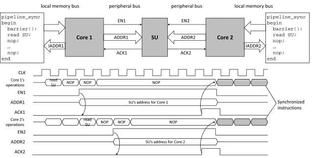
Fig. 9.The synchronization scheme with an example.
Appendix: Processor Synchronization
The purpose of processor synchronization is to ensure that the complementary instructions are executed at the same clock cycle. This requires that not only the instructions but also the processor pipelines are synchronized. For paral-lel programming, we already have a synchronization method barrier that guarantees that any thread/process stops at this point and cannot proceed un-til all other threads/processes reach this barrier. However,barrierdoes not ensure the instructions right after it on different cores start at the same clock cycle. Another synchronization scheme at a lower level is needed. We call it
pipeline sync.
Before presenting our solution, we first introduce a bus protocol used by many processors. The peripheral bus usually has aacksignal which starts from a memory peripheral to the processor. During everyloadoperation, the pro-cessor first uses the address bus and some control signals to send out a memory access request. After that, the selected peripheral uses theacksignal to notify the processor that the required data is ready on the data bus. If the selected pe-ripheral is not able to offer the requested data right away, theacksignal will be kept invalid for a while until the data is ready. When waiting for theacksignal to be valid, the processor is in a fixed state (wait ack).
Our solution makes use of the above memory access protocol, shown in Fig. 9. A Synchronization Unit (SU) is attached to both cores’ peripheral buses. Whenever one core initiates aloadoperation on the SU, theacksignal on its peripheral bus will be kept invalid. This means that every time a core tries to read data from SU, it enters thewait ack state. When both cores are in the
fol-lowing instructions. Moreover, if theacksignal is kept invalid for too long the processing cores consider this as an error and an exception will be launched. To avoid this, we first use a parallel programming’sbarrierto reduce the timing difference of the two cores before doing thepipeline sync. This guarantees no exception occurs. By now, two cores have been totally synchronized. We re-peat the above process every time before running the protected cryptographic software. In this way, the required synchronization is achieved.

![Fig. 2. Processor architecture: (a) Three datapaths in a processor [18]; (b) Datapath forAND operation.](https://thumb-us.123doks.com/thumbv2/123dok_us/1872661.1243720/4.612.145.467.101.215/fig-processor-architecture-datapaths-processor-datapath-forand-operation.webp)