A Push-Push Oscillator Array Using Resonator Type
Coupling Circuits
Takayuki Tanaka1, *, Kengo Kawasaki1, 2, Masayoshi Aikawa1, 3, and Ichihiko Toyoda1
Abstract—A coupled oscillator array using push-push oscillators and resonator type coupling circuits is presented. In the proposed oscillator array, the coupling circuit operates at the fundamental frequency and the output signal is the 2nd harmonics. The adjacent oscillators are connected via the coupling circuits. The coupling circuit is used to synchronize the oscillators and control the phase difference of the output signals. In this study, a three elements push-push oscillator array has been designed in Ku band. The measured phase shift between the output signals of the adjacent oscillators is 511 degrees at the maximum.
1. INTRODUCTION
Recently, an Intelligent Transport Systems (ITS) has been studied to create a traffic system that achieves safety and comfort for drivers. One of the main subjects is a car radar system. An adaptive cruise control system and a collision avoidance radar are very promising applications. A phased array system that achieves electrical beam scanning is indispensable for the car radar systems. The phased array system consists of a local oscillator, a power divider, phase shifters, amplifiers, and antennas. Specially, phase shifters to produce very wide phase shift are necessary for the system. As a result, the system is large, complicated and expensive [1].
On the other hand, a coupled oscillator array has been studied for a power combining method such as quasi-optical power combining and spatial power combining. The original purpose was to obtain high power signals mainly in the millimeter-wave band, using IMPATT diodes, Gunn diodes and FETs [2–5]. Recently, the coupled oscillator array has been studied for electrical beam scanning technique [6–9] and achieves effectively the beam scanning with simple circuit structure. The coupled oscillator array consists of oscillators and coupling networks connecting the oscillators. A push-push oscillator array using an injection locking has been reported by the authors [10, 11]. In the oscillator array, the push-push oscillators are unilaterally synchronized by the injection signals obtained from the oscillators. The signal in the resonator of the oscillator is the injection signal. The signal is injected to the ring resonator of the adjacent oscillator and the phase difference of the output signals is controlled by the phase shift of the injection signal.
In this paper, a novel push-push oscillator array using resonator type coupling circuit [12] is presented. In the oscillator array, reflection type push-push oscillators [13–18] are used for the sub-oscillators. The push-push oscillator consists of two sub-oscillators and one resonator. The oscillator array uses the reflection-waves at the drain ports of the HEMTs used in the sub-oscillators for the controlling of the output phase difference. The method is a new approach for design of the push-push oscillator array. The output signal of the push-push oscillator is the 2nd harmonics of the oscillating signal in the sub-oscillators.
Received 9 September 2014, Accepted 9 October 2014, Scheduled 19 October 2014
* Corresponding author: Takayuki Tanaka ([email protected]).
1 Department of Electrical and Electronic Engineering, Graduate School of Science and Engineering, Saga University, 1 Honjo-machi,
The push-push oscillator array has many advantages by using the push-push oscillators. The output
signal is hard to be affected by change of the loading impedance because the oscillating signal (f0) and
the output signal (2f0) are different. Multi-output ports for the fundamental frequency signal and the
harmonics can be easily inserted to the oscillator. In addition, much higher frequency signal can be generated using inexpensive semiconductor devices for lower frequency applications. These advantages are very useful for oscillator arrays. Moreover, the oscillator array obtains double large phase shift of
the output signals at the second harmonic frequency (2f0) as compared with the phase shift of the
fundamental signal (f0) in the coupling circuit. The push-push oscillators are synchronized at the
fundamental frequency and the phase difference of the output signals are controlled by the coupling circuit. As the structure of the coupling circuit is unsymmetrical, the reflection coefficients at the ports of the coupling circuit are different. The phase shift of the output signals is controlled by the phase difference between the reflection signals at the ports of the coupling circuit. The phase difference between the reflection signals is controlled by the capacitance of the varactor diode mounted on the coupling circuit.
A two elements push-push oscillator array using the coupling circuit has been already reported by authors [12]. Synchronization and phase control between the output signals of adjacent oscillators were confirmed in the oscillator array. This paper presents the basic behavior of the three elements oscillator
array that is the primary trial to realize the multi-elements oscillators array. The three elements
oscillator array is the basic circuit for the multi elements oscillator array because the oscillator array has oscillators arranged in the both ends and the intermediate place. The oscillator array is designed and fabricated in Ku-band. Accordingly, the sub-oscillators and the coupling circuits are designed at the fundamental frequency in C-band due to the push-push principle.
2. PRINCIPLE OF PUSH-PUSH OSCILLATOR ARRAY
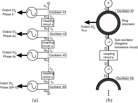
The topology of theN elements oscillator array usingN push-push oscillators is shown in Fig. 1(a). In
the oscillator array, adjacent oscillators are connected using coupling circuits. A push-push oscillator
that generates the second harmonic signal (2f0) for the output is used for the oscillators. Synchronization
between the adjacent oscillators is achieved by the coupling circuit. The phase differences between the output signals are controlled by the coupling circuit as well. Fig. 1(b) shows the structure of the push-push oscillator used for the oscillator and the connection of the oscillators and the coupling circuits.
The push-push oscillator consists of two sub-oscillators, that is a negative resistance circuit (−r), and
a microstrip ring resonator that also plays a role of a power combiner. The active devices used for the sub-oscillators are HEMT. These two sub-oscillators generate the fundamental frequency signals with the same amplitude and 180 degrees phase difference due to the resonant field of the ring resonator. Consequently, the signals of the sub-oscillators are represented by (1) and (2).
V1a = a1ejω0t+a2ej2ω0t+a3ej3ω0t+. . . (1) V1b = a1ej(ω0t+π)+a2ej2(ω0t+π)+a3ej3(ω0t+π)+. . . (2)
These two signals are combined by the power combiner circuit. Therefore, the output signal Vout1
is represented by (3).
Vout1 =A2ej2ω0t+A4ej4ω0t+A6ej6ω0t+. . . (3)
The output signal of the oscillator is the second harmonic signal (2f0) due to the principle of
push-push oscillator, while the synchronization between adjacent oscillators is achieved by the fundamental
frequency signal (f0). The phases of the output signals of oscillator #1 and #2 are synchronized by the
signalV1b in the oscillator #1 and the signalV2ain the oscillator #2 via the coupling circuit between the
oscillators as shown in Fig. 1(a). In the proposed oscillator array, the drain ports of the HEMTs used in the sub-oscillators are connected via the coupling circuit. The phase difference between the reflection coefficients at the ports of the coupling circuit controls the phase difference between the output signals.
The signals of the oscillator #2 is represented by (4) and (5).
)
)
Output 2f0
Phase 0
V1a
Oscillator #1
V1b f0
coupling circuit φ
V2a f0
Oscillator #2 Output 2f0
Phase 2φ
V2b f0
Oscillator #3 Output 2f0
Phase 4φ
V3a f0
V3b
f0
coupling circuit φ
Output 2f0
Phase 2(N-1)φ
VNa VNb Oscillator #N -r Oscillator #1 G
Output 2f0 Vout1
Ring resonator
G
-r Sub-oscillator(Negative
resistance circuit)
D
coupling circuit φ
D
G -r
Oscillator #2 coupling
circuit φ
f0
(a) (b)
Figure 1. Topology of the proposed oscillator array. (a) Push-push oscillator array withN oscillators. (b) Structure of oscillator and the connection.
In the equations, ‘φ’ is the phase shift of the fundamental frequency signal in the coupling circuit.
According to the push-push principle, the output signal of the oscillator #2 is given by (6).
Vout2 =A2ej2(ω0t+φ)+A4ej4(ω0t+φ)+A6ej6(ω0t+φ)+. . . (6) In the output power of push-push oscillators, the second harmonic signal has the largest power compared to all the other harmonics. Therefore, the main output signal of the oscillator #1 and #2 are expressed by (7), (8) from (3) and (6).
Vout1 = A2ej2ω0tej0 (7)
Vout2 = A2ej2ω0tej2φ (8)
Comparing the two output signals, the phase difference is ‘2φ’. When this topology is extended for
N elements oscillator array, the phase difference between the oscillator #1 and #N is ‘2(N −1)φ’ in
principle.
3. COUPLING CIRCUIT
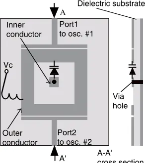
The proposed coupling circuit which connects the adjacent oscillators is described in this section. The push-push oscillator used here has sub-oscillators using HEMTs. The coupling circuits are connected the drain ports. The oscillating frequencies of adjacent oscillators are same by the synchronization using the coupling circuits. Moreover, the phase difference of the reflection coefficients at the ports of the coupling circuit is variable. The phase shift of signals in the coupling circuit can control the phase difference between the output signals of the adjacent oscillators. In the proposed coupling circuit, the large phase shift variation around the resonant frequency is effectively utilized to control the phase difference between the output signals.
of the varactor diode. The structure of the coupling circuit is unsymmetrical. Due to the structure, the resonant frequency at one port (port1) and that at the other port (port2) are different. The phase of the reflection signal at the port2 can be widely changed by the control voltage when the resonant frequency at the port2 is set in around the fundamental frequency of the oscillator. Then, the phase of the reflection signal at the port1 is not changed by the control voltage because the resonant frequency at the port1 is much different from the fundamental frequency. Therefore, the phase difference between the reflection coefficients can be changed by the control voltage. The performance of the coupling circuit is used to control the phase difference between the output signals.
A
Dielectric substrate
Inner conductor
Port1 to osc. #1
Vc
Via hole
Outer conductor
Port2 to osc. #2
A' A-A'cross section
Figure 2. Circuit configuration of the coupling circuit.
La
Port1
Port1
Lg
Port2
Lb Lc
Lc > La
Lc Lb La
Lg
Port2
(a) (b)
Figure 3. Electrical length of the coupling circuit. (a) Equivalent circuit of the coupling circuit. (b) Electrical length related to the resonant frequencies.
An equivalent circuit of the coupling circuit is shown in Fig. 3(a). Fig. 3(b) is the circuit pattern
of the coupling circuit. La, Lb and Lc in Fig. 3(a) correspond ones in Fig. 3(b). La is the electrical
length of the square-shaped resonator. Lb and Lc are the electrical length of a part of the resonator
including the varactor diode. As the structure of the coupling circuit is unsymmetrical, the lengths
that determine the reflection coefficients, Lb and Lc, are different. Due to the equivalent circuit, S11
depends on theLbandS22 depends on theLc. Lgis the length of the microstrip line between the ports
and the gap capacitor. fa, fb and fc are the resonant frequencies determined by the La, Lb and Lc,
respectively.
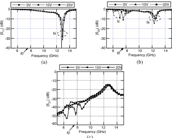
Figure 4 shows the measured scattering parameters of the coupling circuit whenV cis 0 V, 10 V and
20 V. The design frequency (f0) is 7.5 GHz. The circuit is fabricated on a Teflon glass fiber substrate.
port1 and port2 as shown in Figs. 4(a), (b). The resonance of fc is observed at port2 as shown in
Fig. 4(b). The resonant frequencies are 6.32 GHz, 7.09 GHz, and 7.58 GHz when V c is 0 V, 10 V and
20 V, respectively. The resonant frequency fc is controlled by V c. However, fa is not changed by
V c. The transmission characteristics between the adjacent oscillators are shown in Fig. 4(c). The
transmission characteristics at fc (7.5 GHz) is approximately −35 dB and that at fa (12.5 GHz) is
approximately −15 dB.
Figure 5 shows the reflection phase of the coupling circuit at 7.5 GHz which is the operation frequency and the fundamental frequency in the oscillator. In the experiment, the reference planes are set at port1 and port2 as shown in Fig. 3, which are the edge of microstrip line connected to the sub-oscillators. The length between the reference plane and the gap capacitor attached to the resonator,
Lg, is 2 mm. The phase of S11 is almost constant as shown in Fig. 5(a). On the other hand, the phase
ofS22is largely varied by the control voltage as shown in Fig. 5(b). The phase ofS21is almost constant
in the range of the control voltage.
(a)
10V
0V 20V 0V 10V 20V
0
-10
-20
-30
-40
|S | (dB)
11 fa fa fc 0 -10 -20 -30 -40
|S | (dB)
22
6 8 10 12 14
f0 6 f0 8 10 12 14
Frequency (GHz) Frequency (GHz)
10V 0V 20V 0 -10 -20 -30 -40
|S | (dB)
21
-50
-60
6 8 10 12 14
Frequency (GHz)
f0
(b)
(c)
Figure 4. Measured scattering parameters of the coupling circuit with respect to the control voltage
(magnitude, measured). (a) S11. (b)S22. (c)S21.
(a) (b) 50 40 30 20 10 0 -10 -20 -30 -40 -50
Phase S (deg.)
11
0 5 10 15 20 0 5 10 15 20
100 80 60 40 20 0
Phase S (deg.)
22
Control voltage (V) Control voltage (V)
Figure 5. Measured scattering parameters of the coupling circuit with respect to the control voltage
(a) (b)
Figure 6. Surface current density with (Mom) simulation results of the coupling circuit at 7.5 GHz. (a) Input signal from port1. (b) Input signal from port2.
Figure 6 shows the simulated result of surface current density of the coupling circuit by a full-wave simulation of ADS Momentum at 7.5 GHz. The varactor diode is replaced by a shorted line in the simulation. When a signal is input to port1, it is almost reflected. However, when a signal is input
to port2, it is transferred toward the varactor diode. Accordingly, the resonance offc is confirmed at
7.5 GHz. In the proposed coupled oscillator array, the reflection signal from port2 is effectively utilized to control the phase of the output signals.
Table 1. Substrate parameters.
Substrate thickness (h) 0.8 mm
Metal thickness (t) 18µm
Relative dielectric constant (εr) 2.15
Loss tangent (tanδ) 0.001
4. DESIGN AND FABRICATION OF PUSH-PUSH OSCILLATOR ARRAY
The coupled push-push oscillator array using the coupling circuit with unsymmetrical structure is designed and fabricated in Ku band. The circuit is fabricated on a Teflon glass fiber substrate. Fig. 7 shows the circuit pattern of the experimental model of the push-push oscillator array. Fig. 8 shows the fabricated push-push oscillator array with three oscillators. The number of devices, HEMTs and varactor diodes, are extremely reduced compared to the push-push oscillator array using injection locking [11].
The circuit size is 130 mm×25 mm. The circuit consists of a resonator, two sub-oscillators and an
output circuit. The sub-oscillators are negative resistance circuits whose characteristics are same. One
wave length (λg) microstrip ring is used for the resonator. The length between the coupling points of the
.
VDD VDD
Vc
VDD VDD VDD VDD
Vc
Oscillator #1
Output #1
Oscillator #2 Output #2
Oscillator #3 Output #3
Figure 7. Circuit pattern of the push-push oscillator array.
Figure 8. Fabricated push-push oscillator array.
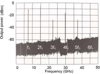
Figure 9. Output power spectrum of the oscillator #1 in full span of 50 GHz with a 10 dB attenuator when the control voltage is 6.0 V.
5. EXPERIMENT
The output power and the oscillating frequency of each push-push oscillator and the phase difference between the output signals of adjacent oscillators are measured. The phase difference between the
output signals of the oscillator #1 and #2 is represented by φ12. That between the oscillator #2 and
#3 is represented byφ23. The drain bias voltage of each oscillator is 3.5 V. The gate bias voltage is 0 V.
The total operating current of the oscillator array is 0.25 A. The bias voltage of the varactor diode, which is the control voltage for the phase shift, is supplied to each varactor diode in common. Fig. 9 shows the experimental result of the output power spectrum of the oscillator #1 when the control voltage is 6.0 V. A spectrum analyzer is used to measure the output power and the oscillating frequency. Then a 10 dB attenuator is used for the measurement. The phase shift control of the output signals of adjacent oscillators are performed with the range of the control voltage from 6.0 V to 18 V. The maximum output powers of oscillator #1, oscillator #2 and oscillator #3 are +7.00 dBm, +6.67 dBm and +7.50 dBm, respectively. The powers are almost same.
of the three oscillators versus the control voltage. The oscillating frequency of the oscillator #1 varies from 14.732 GHz to 14.763 GHz. That of the oscillator #2 is from 14.759 GHz to 14.799 GHz. That of the oscillator #3 is from 14.703 GHz to 14.766 GHz. The variations are very small. Therefore, the push-push oscillators are synchronized effectively.
Figure 11 shows the phase noise performance of the oscillator #1 with a 10 dB attenuator when
the control voltage is 6.0 V. The phase noise at the offset frequency of 100 kHz is −81.0 dBc/Hz. The
phase noises of these three oscillators are −103.5 dBc/Hz, −95.8 dBc/Hz, and −108.0 dBc/Hz at the
offset frequency of 1 MHz and −81.0 dBc/Hz, −72.2 dBc/Hz, and−81.7 dBc/Hz at the offset frequency
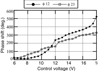
of 100 kHz. The phase difference between the output signals of adjacent oscillators is measured. In the measurement, a double balanced mixer and the oscilloscope are used. The output signals of oscillators are down converted by the double balanced mixers, and the phase difference between the output signals are measured. The input LO frequency is 14.500 GHz with the output power of 0 dBm. Fig. 12 shows the phase differences between the signals of adjacent oscillators versus the control voltage. The phase
differenceφ12 between the oscillator #1 and #2 is from +13 degrees to +524 degrees. The phase shift
is 511 degrees. The phase differenceφ23 between the oscillator #2 and #3 is from +15 degrees to +328
degrees. The phase shift is 313 degrees. It is considered that the difference is caused by the difference of free running frequency of each push-push oscillator due to the asymmetrical circuit configuration of the oscillators including the coupling circuits and the individual difference of the varactor diodes. In addition, very wide output phase shift is obtained. It is considered that the change of the phase differences of output signals is achieved by both the reflection phase shift and the change of the reflection
amplitude of the fundamental signal (f0) obtained in the coupling circuit at the resonant frequency.
Table 2 shows the output power of the 2nd harmonics and the suppression of the undesired signals of each oscillator. The suppression of the undesired fundamental signals of the three oscillators
(a) (b)
Oscillator#1 Oscillator#2 Oscillator#3 Oscillator#1 Oscillator#2 Oscillator#3
8.0
7.5
7.0
6.5
6.0
5.5
5.0
Output power (dBm)
14.9
14.8
14.7
14.6
Oscillating frequency (GHz)
6 8 10 12 14 16 18 6 8 10 12 14 16 18
Control voltage (V) Control voltage (V)
Figure 10. Output power and oscillating frequency of each push-push oscillator vs. control voltage. (a) Output power. (b) Oscillating frequency.
Figure 11. Output power spectrum for
estimating phase noise of the oscillator #1 (V c=
6.0 V, span: 10.0 MHz, RBW: 10 kHz, VBW:
1 kHz).
φ 12 φ 23
600 500 400 300 200 100 0
Phase shift (deg.)
6 8 10 12 14 16 18
Control voltage (V)
Figure 12. Output phase shift vs. control
voltage (φ12: phase difference between oscillator
#1 and oscillator #2, φ23: phase difference
Table 2. Output power and suppression of undesired harmonics (control voltage is 0 V).
Oscillator #1 Oscillator #2 Oscillator #3
f0 (suppression) −6.83 dBc −20.16 dBc −21.33 dBc
2f0 (output power) +6.33 dBm +6.17 dBm +6.83 dBm
3f0 (suppression) −21.33 dBc −21.33 dBc −21.67 dBc
4f0 (suppression) −14.00 dBc −20.50 dBc −9.33 dBc
5f0 (suppression) −23.66 dBc −38.33 dBc −28.00 dBc
are −6.83 dBc, −20.16 dBc, and −21.33 dBc, respectively. Undesired odd harmonics as well as the
fundamental signal are also suppressed. The output power of the fourth harmonic signal is relatively higher than that of the other odd harmonic signals due to the push-push principle. In the results, the suppressions of fundamental signals of oscillators are different. The reflection coefficients at the ports of the coupling circuit are different because of the asymmetrical circuit configuration. Moreover, the combinations of reflection coefficients at the drain ports of HEMTs are different between the oscillator #1 and the oscillator #3. Therefore, the suppressions of the fundamental signals of the oscillators are different.
The proposed push-push oscillator array achieves synchronization of the adjacent oscillators and excellent output phase shift over 300 degrees.
6. CONCLUSION
A coupled push-push oscillator array using resonator type coupling circuits is studied, and its basic behavior of the three elements push-push oscillator array is demonstrated. The three elements oscillator array has oscillators arranged in both end places and intermediate place. The structure is basic one to study multi-elements push-push oscillator array, which is the first investigation. In the circuit, resonator type coupling circuits with unsymmetrical structure is used for the synchronization and the phase control between the adjacent oscillators. The number of devices, HEMTs and varactor diodes, are extremely reduced compared to the push-push oscillator array using injection locking. It is confirmed that the three elements push-push oscillator array achieves good results. In the experiment, much phase shift between the output signals of the adjacent oscillators is obtained. Therefore, the proposed oscillator array is very promising to realize wide beam scanning for radar systems.
ACKNOWLEDGMENT
This work was supported by JSPS KAKENHI Grant Number 24560409.
REFERENCES
1. Hansen, R. C., Phased Array Antennas, John Wiley & Sons, 1998.
2. York, R. A. and R. C. Compton, “Quasi-optical power combining using mutually synchronized
oscillator arrays,” IEEE Trans. Microw. Theory Tech., Vol. 39, No. 6, 1000–1009, Jun. 1991.
3. Mortazawi, A., H. D. Foltz, and T. Itoh, “A periodic second harmonic spatial power combining
oscillator,” IEEE Trans. Microw. Theory Tech., Vol. 40, No. 5, 851–856, May 1992.
4. Birkeland, J. and T. Itoh, “A 16 element quasi-optical FET oscillator power combining array with
external injection locking,”IEEE Trans. Microw. Theory Tech.,Vol. 40, No. 3, 475–481, Mar. 1992.
5. Kormanyos, B. K. and G. M. Rebeiz, “20-GHz power combining slot-oscillator array,”IEEE Trans.
6. Liao, P. and R. A. York, “A new phase-shifterless beam-scanning technique using array of coupled
oscillators,” IEEE Trans. Microw. Theory Tech., Vol. 41, No. 10, 1810–1815, Oct. 1993.
7. Pogorzelski, R. J., P. F. Maccarini, and R. A. York, “A continuum model of the dynamics of coupled
oscillator arrays for phase-shifterless beam scanning,”IEEE Trans. Microw. Theory Tech.,Vol. 47,
No. 4, 463–470, Apr. 1999.
8. Nogi, S., M. Sanagi, and K. Fujimori, “Active integrated antenna techniques for beam control,” IEICE Trans. Electron., Vol. E88-C, No. 7, 1358–1367, Jul. 2005.
9. Georgiadis, A. and A. Collado, “Injection locked coupled oscillator arrays,”IEEE Trans. Microwave
and Wireless Components Lett., Vol. 17, No. 12, 900–902, Dec. 2007.
10. Kawasaki, K., T. Tanaka, and M. Aikawa, “A unilaterally coupled push-push oscillator array
using sequential injection-locking,” Proc. of Asia-Pacific Microwave Conference 2011, 868–871,
Dec. 2011.
11. Kawasaki, K., T. Tanaka, and M. Aikawa, “A sequential Injection locked coupled push-push
oscillator array using unilateral coupling circuit,”IEICE Trans. Electron., Vol. E95-C, No. 9, 1535–
1542, Sep. 2012.
12. Kawasaki, K., T. Tanaka, and M. Aikawa, “Ku band second harmonic N-coupled push-push
oscillator array using microstrip resonator,” IEEE MTT-S Int. Microw. Symp. Digest, 1182–1185,
May 2010.
13. Pavio, A. M. and M. A. Smith, “A 20-40-GHz push-push dielectric resonator oscillator,” IEEE
Trans. Microw. Theory Tech., Vol. 33, No. 12, 1346–1349, Dec. 1985.
14. Sinnesbichler, F. X., “Hybrid millimeter-wave push-push oscillators using silicon-germanium
HBTs,”IEEE Trans. Microw. Theory Tech., Vol. 51, No. 2, 422–430, Feb. 2003.
15. Wanner, R., H. Schafer, R. Lachner, G. R. Olbrich, and P. Russer, “A fully integrated 70 GHz SiGe
low phase noise push-push oscillator,”IEEE MTT-S Int. Microw. Symp. Digest, Vol. 3, 1523–1526,
Jun. 2005.
16. Kawahata, K., T. Tanaka, and M. Aikawa, “A K-band push-push oscillator with high suppression
of undesired harmonic signals,” IEICE Trans. Electron., Vol. E86-C, No. 8, 1433–1437, Aug. 2003.
17. Xiao, H., T. Tanaka, and M. Aikawa, “Push-push oscillator with simplified circuit structure,”IEE
Electron. Lett., Vol. 38, No. 24, 1545–1547, Nov. 2002.
18. Xiao, H., T. Tanaka, and M. Aikawa, “A 20 GHz push-push oscillator using ring resonator, ”IEICE