Reduction of Mutual Coupling between Cavity-Backed
Slot Antenna Elements
Qi-Chun Zhang, Jin-Dong Zhang, and Wen Wu*
Abstract—Maintaining mutual coupling suppressing structure as simple as possible is becoming attractive in the electromagnetic and antenna community. A novel parasitic patch structure that can reduce mutual coupling between cavity-backed slot antenna elements is proposed and studied. The structure consists of only a simple rectangular patch inserted between the antenna elements, and it is therefore low cost and straightforward to fabricate. The proposed structure can not only suppress the surface-mode propagation and reduce mutual coupling between slot antennas, but also improve radiation patterns. The features include small occupied area and very simple structure.
1. INTRODUCTION
The mutual coupling (MC) or isolation has a direct impact on a number of applications. These include antenna array systems and more recently multiple input multiple output (MIMO) wireless communication systems [1]. Often, applications of planar antenna elements integrated on high dielectric constant substrates are of special interest due to their compact size and conformability with monolithic microwave integrated circuit (MMIC). However, the utilization of a high dielectric constant substrate has some drawbacks, such as a narrower bandwidth and pronounced surface wave. The bandwidth can be recovered by using a thick substrate, yet this excites severe surface wave. The generation of surface wave can lead to coupling between adjacent antenna elements. Moreover, it decreases the antenna efficiency and distorts radiation patterns. This paper concentrates on the surface wave suppression of the parasitic structure and the mutual coupling reduction of the cavity-backed slot antennas.
Several schemes have been proposed to reduce the effects of surface wave. Some are the investigations of surface wave suppression for a single antenna element. The others are used in the special applications including MIMO antennas and arrays for low mutual coupling and improved radiation performance. Xiao et al. [2] have suggested back-to-back U-shaped defected ground structures (DGS). For the reported design in [3, 4], shorted patches were used to prevent excitation of the surface wave mode. In [5–7], electromagnetic band-gap (EBG) structures were proposed to suppress mutual coupling. However, they are complex structures, and optimum designs are more difficult to achieve. The effects of superstrate materials on printed circuits antennas were investigated in [8]. With a proper choice of superstrate properties and dimensions, surface waves can be eliminated. But the substrate must be electrically thin, at least for nonmagnetic superstrates. Another approach suggested minimizing surface-wave propagation is to use a synthesized substrate that lowers the effective dielectric constant of the substrate either under or around the patch [9–11]. The difficulty with these schemes is that it needs an extra fabrication technique. The detailed comparisons between the techniques presented in the literature and the method proposed in this paper are listed in Table 1.
A two-element antenna is used, and an isolation as high as possible is needed between transmit and receive antenna in the field of MIMO technology and radar applications. This can be seen in the
Received 29 May 2014, Accepted 5 August 2014, Scheduled 20 August 2014 * Corresponding author: Wen Wu ([email protected]).
Table 1. Comparisons between methods.
Paper Method Implement Surface Wave
Reduction
Radiation Improvement
[2] DGS Easy ↑↑ ↑
[3, 4] Short patch Normal ↑↑ —
[5–7] EBG Hard ↑ —
[8] Superstrate Normal ↑↑ ↑
[9–11] Synthesized Substrate Hard ↑ ↑
This paper Parasitic patch Easy ↑ ↑
large number of publications using two-element structures, including [2] and [4–7]. This requirement is driving our research to study a new way for reducing mutual coupling between cavity-backed slot antennas in satellite communication system. Although much work has been carried out for reducing mutual coupling using parasitic elements [12], little has been reported for suppressing surface wave effect employing parasitic elements. In this paper, we describe a simple but highly effective parasitic structure to eliminate surface waves in the substrate, and then MC between inverted cavity-backed slot antenna elements [13–15] is reduced. The parasitic structure is a patch etched on the top side of the substrate next to the long edge of the cavity. The coupling reduction bandwidth fully covers the operating bandwidth of the antennas. Furthermore, the proposed structure can improve radiation patterns of the elements and enhance antennas gain. It can be easily fabricated without extra cost.
2. PROPOSED PARASITIC PATCH STRUCTURE
2.1. Antenna Structure
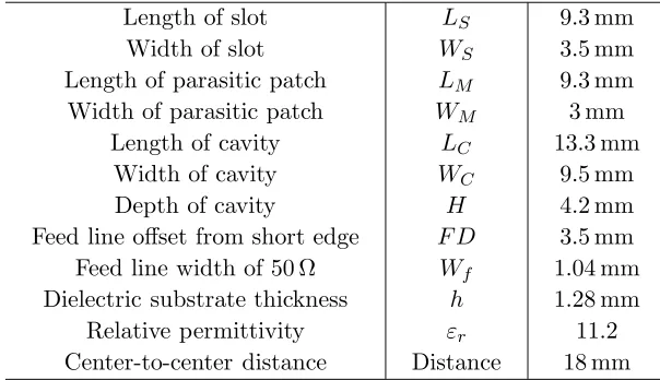
Based on the principle of reducing mutual coupling in the previous section, a dual-element slot antenna with parasitic element is designed in this section. The center-to-center distance between the elements is 0.72λ0. The geometry of the proposed parasitic structure is shown in Fig. 1. Two slots are etched on the bottom layer of a RT/duroid 3010 substrate and backed by two metallic rectangular cavities to reduce the backward radiation. The thickness of the substrate is 1.28 mm, and its dielectric constant is 11.2. Each slot antenna operating 12 GHz band is fed by a 50-Ω microstrip line. The microstrip lines are printed on the top side of the substrate.
In order to reduce the mutual coupling, a parasitic patch etched on the upper layer of the substrate is placed between the two antenna elements. The detailed parameters are listed in Table 2.
Table 2. Geometrical parameters of the proposed dual-element slot antenna.
Length of slot Width of slot Length of parasitic patch
Width of parasitic patch Length of cavity
Width of cavity Depth of cavity
Feed line offset from short edge Feed line width of 50 Ω Dielectric substrate thickness
Relative permittivity Center-to-center distance
LS WS LM WM LC WC H F D
Wf h εr Distance
9.3 mm 3.5 mm 9.3 mm 3 mm 13.3 mm
9.5 mm 4.2 mm 3.5 mm 1.04 mm 1.28 mm
LS
WM
WS
Wf WC
F
L
M
L
C
FD
Distance
Feeding line Parasitic element
Metallic cavity Ground
Slot Slot
Air Air
h
H
(a) (b)
(c)
Figure 1. Structure of the dual-element slot antenna with parasitic element. (a) Top view. (b) Side view. (c) Photo.
2.2. Parametric Studies
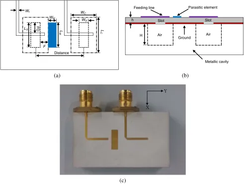
To understand the design tradeoffs of the proposed structure, parametric studies of this parasitic patch structure have also been performed. Through parameters sweeps and optimizations, it is found that three parameters —F,WM, and LM — are important in this design.
At first, in order to simplify design, the parasitic patch placed at the center between the left slot and right side feed line can be located next to long edge of the cavity. The influences of other parameters, WM and LM, are listed in Figs. 2–5.
The main aim of the proposed paper is to reduce mutual coupling and enhance antenna gain. The mutual coupling and antenna gain (the left side antenna) at the operating frequency along with the parameter WM are shown in Fig. 2 and Fig. 3, when the other parameters are LS = 9.3 mm, WS= 3.5 mm, F = 3 mm, LM = 9.3 mm. It is observed that antenna gain of this structure is sensitive to WM. The maximum gain appears whenWM is equal to 3 mm, which is close to the half-wavelength in substrate of the resonant frequency. The mutual coupling is low whenWM is equal to 3 mm.
1.5 2.0 2.5 3.0 3.5 4.0 4.5 -32 -30 -28 -26 -24 -22 -20 -18 -16 -14 |S21 | ( d B )
WM (mm)
Figure 2. Mutual coupling varying with the parameterWM.
1.5 2.0 2.5 3.0 3.5 4.0 4.5
0 1 2 3 4 5 6 Ga in ( d B )
WM (mm)
Figure 3. Antenna gain varying with the parameterWM.
5 6 7 8 9 10 11 12 13 14
-32 -30 -28 -26 -24 -22 -20 -18 -16 |S21 | ( d B )
LM (mm)
Figure 4. Mutual coupling varying with the parameterLM.
5 6 7 8 9 10 11 12 13 14
1 2 3 4 5 6 7 Ga in ( d B )
LM (mm)
Figure 5. Antenna gain varying with the parameterLM.
3. SIMULATED AND MEASURED RESULTS
3.1. S Parameters
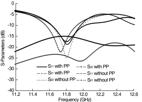
Theoretical simulations are performed using ANSYS high frequency structure simulator (HFSS) ver. 13 to optimize the antenna parameters for desired performance. The simulated S-parameter comparisons between the normal dual-element slot antennas and the proposed slot antenna are shown in Fig. 6. The reflection coefficient of the individual antenna element is not affected significantly after adding parasitic patch. However, mutual coupling between the two antenna elements is greatly reduced, especially in the operating band centered at 12 GHz. For the structure without parasitic patch, in this region mutual coupling is higher than −15 dB, as shown in the figure. By using an optimized parasitic patch, the coupling is significantly improved, to less than −23 dB, with an improvement of minimum 7 dB, exceeding 9 dB at many frequency points over the operating band. It can be seen that the improvement has been achieved in a wide bandwidth, adequate for a typical satellite communication application.
11.2 11.4 11.6 11.8 12.0 12.2 12.4 12.6 -40 -35 -30 -25 -20 -15 -10 -5 0
S11 with PP S22 with PP S21 with PP S11 without PP S22 without PP S21 without PP
S -P a ra m e te rs (d B ) Frequency (GHz)
Figure 6. Simulated reflection coefficient and mutual coupling results of the antenna elements (“PP” means parasitic patch).
11.2 11.4 11.6 11.8 12.0 12.2 12.4 12.6 -45 -40 -35 -30 -25 -20 -15 -10 -5 0
S11 with PP S22 with PP S21 with PP S11 without PP S22 without PP S21 without PP
S-Pa ra m e te rs ( d B) Frequency (GHz)
Figure 7. Measured reflection coefficient and mutual coupling results of the antenna elements.
11.2 11.4 11.6 11.8 12.0 12.2 12.4 12.6 -40 -35 -30 -25 -20 -15 -10 -5 0
S11 with PP S22 with PP S21 with PP S11 without PP S22 without PP S21 without PP
S-Pa ra m e te rs ( d B) Frequency (GHz)
Figure 8. Simulated reflection coefficient and mutual coupling results of the antenna elements when the dielectric constant is 11.6.
0.5 0.6 0.7 0.8 0.9 1.0 1.1
-21 -20 -19 -18 -17 -16 -15 -14 -13 |S21 | ( d B )
Distance (λ)
Figure 9. The simulated mutual coupling varying with the slot distance at the resonant frequency.
acquired over a wide frequency band. The difference between measured and simulated results is mainly caused by the shift in resonant frequencies. This frequency shift is mainly attributed to the dielectric constant of the substrate. The simulated S-parameter results with the permittivity of 11.6 are shown in Fig. 8. The results validate the reason of frequency shift.
Figure 9 shows the mutual coupling between the normal dual-element slot antennas varying with the slot distance at the resonant frequency by the simulation. The mutual coupling decreases as the antenna distance increases. Meanwhile, it is observed that the case has a strong mutual coupling level. This is because the slot antennas on a high permittivity and thick substrate activate severe surface waves.
coupling (a relatively fast method) to evaluate the ECC (1) [17] in this paper
ρe=|ρc|2 ∼=|r12|2 =
Re(Z12) Re(Z11)
2 (1)
The mutual impedance (Z12) can be easily determined from the standard S-parameters of the two-port antenna system. From (1) we obtain that the envelope correlation of the parasitic structure is 0.1336, with an improvement about 0.2 for the normal dual-antennas at the trough of the measured reflection coefficient curves.
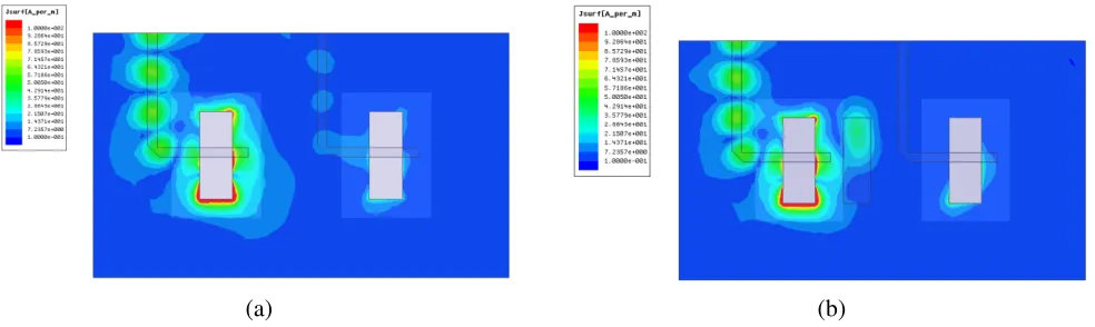
3.2. Surface Current Distributions
In Section 2, we adopted parasitic element to reduce mutual coupling and implemented the technique in a dual-cavity-slot-element antenna. In order to better understand the mechanism, HFSS is employed to plot the surface current distributions along the slot antennas.
The performance of reducing mutual coupling can be validated with surface current magnitude distributions. The current magnitude distributions over the surface of the normal dual-slot antenna at 12 GHz are shown in Fig. 10(a). Slot element 1 (the left side slot antenna) is excited while slot antenna 2 (the right side slot antenna) is terminated with a matched load. As a comparison task, the surface current magnitude distributions of the proposed parasitic structure are also provided in Fig. 10(b). From Fig. 10, it can be seen that the current distributions on slot antenna 2 decrease dramatically by adding the parasitic patch, validating the principle analysis of reducing mutual coupling by creating a reverse coupling path in [12].
(a) (b)
Figure 10. The current magnitude distribution over the surfaces. (a) Without the parasitic patch. (b) With the parasitic patch.
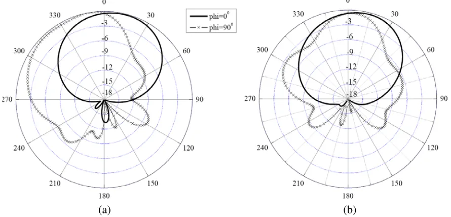
3.3. Radiation Pattern
(a) (b)
Figure 11. Effect of parasitic patch on the copolar radiation pattern. (a) Simulation, at 12 GHz, port 1 feed, phi = 0◦. (b) Simulation, at 12 GHz, port 2 feed, phi = 90◦.
(a) (b)
Figure 12. Measured radiation patterns of the parasitic structure. (a) At 11.8 GHz, port 1 feed, phi = 0◦. (b) At 11.8 GHz, port 2 feed, phi = 90◦.
4. CONCLUSION
REFERENCES
1. Chiu, C.-Y., C.-H. Cheng, R. D. Murch, and C. R Rowell, “Reduction of mutual coupling between closely-packed antenna elements,” IEEE Trans. Antennas Propag., Vol. 55, No. 6, 1732–1738, Jun. 2007.
2. Xiao, S., M.-C. Tang, Y.-Y. Bai, S. Gao, and B.-Z. Wang, “Mutual coupling suppression in microstrip array using defected ground structure,”IET Microw. Antennas Propag., Vol. 5, No. 12, 1488–1494, 2011.
3. Jackson, D. R., J. T. Williams, A. K. Bhattacharyya, R. L. Smith, S. J. Buchheit, and S. A. Long, “Microstrip patch designs that do not excite surface waves,” IEEE Trans. Antennas Propag., Vol. 41, No. 8, 1026–1037, Aug. 1993.
4. Khayat, M. A., J. T. Williams, D. R. Jackson, and S. A. Long, “Mutual coupling between reduced surface-wave microstrip antennas,” IEEE Trans. Antennas Propag., Vol. 48, No. 10, 1581–1593, Oct. 2000.
5. Yang, F. and Y. Rahmat-Samii, “Microstrip antennas integrated with electromagnetic band-gap (EBG) structures: A low mutual coupling design for array applications,” IEEE Trans. Antennas
Propag., Vol. 51, No. 10, 2936–2946, Oct. 2003.
6. Yang, L., M. Y. Fan, F. L. Chen, J. Z. She, and Z. H. Feng, “A novel compact electromagnetic-bandgap (EBG) Structure and its applications for microwave circuits,” IEEE Trans. Antennas
Propag., Vol. 53, No. 1, 183–190, Jan. 2005.
7. Coulombe, M., K. S. Farzaneh, and C. Caloz, “Compact elongated mushroom (EM)-EBG structure for enhancement of patch antenna array performances,” IEEE Trans. Antennas Propag., Vol. 58, No. 4, 1076–1086, Apr. 2010.
8. Alexopoulos, N. G. and D. R. Jackson, “Fundamental superstrate (cover) effects on printed circuit antennas,”IEEE Trans. Antennas Propag., Vol. 32, No. 8, 807–816, Aug. 1984.
9. Gauthier, G. P., A. Courtay, and G. H. Rebeiz, “Microstrip antennas on synthesized low dielectric-constant substrate,” IEEE Trans. Antennas Propag., Vol. 45, No. 8, 1310–1314, Aug. 1997. 10. Papapolymerou, I., R. F. Frayton, and L. P. B. Katehi, “Micromachined patch antennas,” IEEE
Trans. Antennas Propag., Vol. 46, No. 2, 275–283, Feb. 1998.
11. Colburn, J. S. and Y. Rahmat-Samii, “Patch antennas on externally perforated high dielectric constant substrates,”IEEE Trans. Antennas Propag., Vol. 47, No. 12, 1785–1794, Dec. 1999. 12. Li, Z., Z. Du, M. Takahashi, K. Satio, and K. Ito, “Reduction mutual coupling of MIMO antennas
with parasitic elements for mobile terminals,” IEEE Trans. Antennas Propag., Vol. 60, No. 2, 473–481, Feb. 2012.
13. Li, Q. and Z. Shen, “Inverted microstrip-fed cavity-backed slot antenna,”IEEE Antennas Wireless
Propag. Lett., Vol. 1, 190–192, 2002.
14. Zheng, B. and Z. Shen, “Effect of a finite ground plane on microstrip-fed cavity-backed slot antenna,” IEEE Trans. Antennas Propagat., Vol. 53, 862–865, Feb. 2005.
15. Liu, Y. and Z. Shen, “A compact dual-band cavity-backed slot antenna,”IEEE Antennas Wireless
Propag. Lett., Vol. 5, 4–6, 2006.
16. Ko, S. C. K. and R. D. Murch, “A diversity antenna for external mounting on wireless handsets,”
IEEE Trans. Antennas Propagat., Vol. 49, 840–842, May 2001.
17. Vaughan, R. G. and J. B. Andersen, “Antenna diversity in mobile communications,”IEEE Trans.