A Modified Coupled-Line Schiffman Phase Shifter
with Short Reference Line
Weiwei Zhang1, *, Yuanan Liu1, Yongle Wu1, 2, Weimin Wang1, Ming Su1, and Jinchun Gao1
Abstract—A coupled-line circuit structure is proposed in this paper to design a modified Schiffman phase shifter with short reference line. Based on the traditional transmission line theory and ABCD parameters, closed-form mathematical equations for electrical and scattering parameters are obtained. Obviously, this proposed coupled-line phase shifter has several advantages such as arbitrary phase difference, easy implementation, and analytical design method. Finally, two examples of microstrip coupled-line phase shifter, which have fractional bandwidth over 45%, are fabricated and measured. Good agreements between the simulated and measured results verify our design.
1. INTRODUCTION
Phase shifter, as an important microwave component, has been widely used in the design of wideband phase-array antennas, Butler matrices [1, 2] which consist of 90◦ hybrids and phase shifters, couplers [3] which are a combination of coupled-line power divider and improved coupled-line phase shifter, etc. Phase shifters are mainly categorized into three types: mechanical phase shifters, ferrite phase shifters and semiconductor device phase shifters. In this paper only some planar phase shifters are discussed.
One important type is load-line phase shifter [4–7]. The digital loaded-line phase-shift network [4], which uses the loads to change the electrical length of a fixed transmission line, is used to design two types of microwave hybrid thin-film phase shifters. Digital diode-loaded-line phase shifters is described in [5]. It shows that a 75◦ separation between the loading susceptances has the same or better performance than a 90◦ separation. In addition, analytical equations for a loaded-line phase shifter are derived, and it is shown that the maximum bandwidth is obtained when the spacing between the switched susceptances is 90◦ in [6]. By utilizing a phasor diagram representation of the line, the circuit design procedure for the loaded-line phase shifter is presented in [7].
Another important type of phase shifter structure is firstly described by Schiffman in [8]. By proper selection of the length of these lines and coupling coefficients, the phase difference can be made to be almost constant over a broad bandwidth. However, the Schiffman phase shifter requires a tight coupling in the coupled line sections. Therefore, the improved Schiffman phase shifters [9] shows that different configurations can be used to design differential phase shifters with loose coupled lines and the same performance as for the standard case. The analysis of a phase-shift network is given in [10]. This network consists of a cascade of N pairs of coupled transmission lines connected together at their far end with different electrical lengths. General synthesis procedures are given to determine its phase deviation and maximum bandwidth when the coupling coefficients are known, or to determine the coupling coefficients for a desired bandwidth or maximum phase deviation [11]. Moreover, [12] shows significant differences in theoretical performance by using an exact analysis in terms of odd and even mode propagation velocities. In order to cancel the influence of the even-odd phase velocity, a novel method is put forward
Received 30 June 2014, Accepted 1 September 2014, Scheduled 3 October 2014 * Corresponding author: Weiwei Zhang ([email protected]).
in [13] by choosing the characteristic impedance and electrical length of the linking line between the coupled lines. In addition, there are many methods to improve the bandwidth of the Schiffman phase shifter, such as multi-section cascading connection [14, 15], utilizing the unique frequency-independent quadrature property of symmetric couplers [16], and using two 90◦ parallel coupled lines [17]. Besides, there are other phase shifter structures, such as a broadband phase shifter which employs loaded λ/4 transmission line [18], single-layer ultra wideband 90◦ differential phase shifter whose main line consists of a multi-section radial TL in the middle [19], etc. However, these circuit structures of the phase shifters are complex and very large.
Especially, the conventional Schiffman phase shifter [8, 9] can be used to achieve flat relative-phase differences between output ports. However, these circuits require long reference lines and tight coupled sections which are difficult to realize. Compared with the circuits in [8, 9], this proposed modified Schiffman phase shifter, composed of only two different coupled lines with weak coupling coefficients, can realize arbitrary phase difference by changing the reference line when the main line is fixed. This novel phase shifter offers several advantages, including: 1) arbitrary phase difference; 2) short reference line; 3) weak coupled sections; 4) all ports matched; 5) analytical design equations for circuit electrical parameters and scattering parameters; and 6) easy realization in the common microstrip technology. In Section 2, closed-form design equations and scattering parameters are derived using conventional transmission line theory andABCD parameters. For observation of the phase difference at the operating frequency and the influence of electrical parameters, six examples will be discussed in the Section 3. Two experimental microstrip circuits are fabricated and measured in Section 4. The consistency between the calculated and simulated results validates this proposed phase shifter.
2. CIRCUIT STRUCTURE AND DESIGN THEORY
Figure 1 shows the proposed circuit structure of the modified Schiffman phase shifter, which is composed of two different coupled lines. The coupled-line parameters include even-mode characteristic impedances (Ze1, Ze2), and odd-mode characteristic impedances (Zo1, Zo2). For simplification, the even and odd electrical lengths are assumed to be the same. In addition, each port impedance is denoted byZ0.
Port 1 Port 2
Port 3 Port 4
Main line
Reference line
Ze1, Zo1,θ1
Ze2, Zo2,θ2
Yin
Z0
Z0
Z0
Z0
Figure 1. The proposed modified coupled-line Schiffman phase shifter.
2.1. Analytical Design Equations of the Phase Shifter
According to [20],ABCD parameter of the coupled line connected at one end is:
Ai Bi Ci Di
=
⎡ ⎢ ⎢ ⎣
Zeicotθi−Zoitanθi Zeicotθi+Zoitanθi
2jZeiZoi Zeicotθi+Zoitanθi 2j
Zeicotθi+Zoitanθi
Zeicotθi−Zoitanθi Zeicotθi+Zoitanθi
⎤ ⎥ ⎥
The ideal matching at the operation frequency is necessary, and the corresponding scattering parameters can be expressed as follows:
Sii= 0, (i= 1,2,3,4) (2)
The scattering parameters of the main line can be obtained in terms ofABCD parameters in [21]:
S11 =
A1+B1/Z0−C1Z0−D1 A1+B1/Z0+C1Z0+D1
, (3a)
S12 = S21=
2
A1+B1/Z0+C1Z0+D1
, (3b)
S22 = −
A1+B1/Z0−C1Z0+D1 A1+B1/Z0+C1Z0+D1
. (3c)
After substituting (1), (3) into (2) and some simple linear mathematical operation, the following equation can be obtained:
Ze1Zo1=Z02 (4)
Then the scattering parameters of the main line at the operating frequency in Equation (3) can be simplified:
S11 = S22= 0, (5a)
S21 = S12=
Ze1cotθ1+Zo1tanθ1 Ze1cotθ1−Zo1tanθ1+j2Z0
=ejψ1, (5b)
where the phase shifter Ψ1 is defined by:
cosψ1=
g1−tan2θ1 g1+ tan2θ1
,
g1= Ze1 Zo1
. (6)
For the reference line in Figure 1, the scattering parameters can also be obtained in terms ofABCD parameters in [21]:
S33 =
A3+B3/Z0−C3Z0−D3 A3+B3/Z0+C3Z0+D3
, (7a)
S34 = S43=
2
A3+B3/Z0+C3Z0+D3
, (7b)
S44 = −
A3+B3/Z0−C3Z0+D3 A3+B3/Z0+C3Z0+D3
. (7c)
where
A3 B3 C3 D3
=
1 0
Yin 1
. (8)
According to the transmission line theory, we can obtain the following equation:
Yin= C2ZL+D2 A2ZL+B2
ZL=∞
= 2j
Ze2cotθ2−Zo2tanθ2
(9)
After substituting Equations (1), (7), (8), and (9) into (2), the following equation can be obtained:
θ2 =n π
2(n= 1,2,3, . . .) (10)
Then the scattering parameters of the reference line at the operating frequency in Equation (7) can be simplified:
S33 = S44= 0, (11a)
S43 = S34= 1. (11b)
2.2. Scattering Parameters and the Phase Difference
From Section 2.1, this proposed circuit structure can be designed analytically according to Equations (4), (10). The scattering parameters and phase difference will be given in this section.
After substituting Equations (1), (4), (8), and (9) into Equations (3) and (7), the scattering parameters will be obtained as follows:
S11 = S22= 0, (12a)
S21 = S12=
Ze1cotθ1+Zo1tanθ1 Ze1cotθ1−Zo1tanθ1+j2Z0
, (12b)
S33 = S44= −
jZ0
(Ze2cotθ2−Zo2tanθ2) +jZ0
, (12c)
S43 = S34=
Ze2cotθ2−Zo2tanθ2 (Ze2cotθ2−Zo2tanθ2) +jZ0
. (12d)
From Equations (12), a conclusion thatS11,S22 are independent of the frequency can be obtained. The phase difference at the operating frequency can be calculated as follows:
Δθ=phase(S21)−phase(S43) =ψ1. (13)
Equation (13) means that the phase difference Δθat the operating frequency only depends on the main line. Nevertheless, the fractional bandwidth lies on the whole circuit.
3. ANALYSIS OF CIRCUIT ELECTRICAL PARAMETERS
Based on the previous theoretical analysis, the electrical parameters of the proposed circuit can be easily calculated according to Equations (4), (6), and (10). For observation of the phase difference at the operating frequency and influence of the electrical parameters, six examples will be discussed in this section.
3.1. The Discussion of the Phase Difference Δθ
According to Equation (12), the phase difference at the operating frequency is only decided by the main line. From Figure 2(a), it can be observed that whenθ1 varies from 0◦to 180◦, the phase shift Δθof the proposed circuit varies from 360◦ to 0◦, monotonously. Though the impedance ratio g1 of the coupled line increases from 1.2 to 1.9, the phase difference Δθ changes slightly. The effect of g1 and θ1 on the bandwidth of the phase shifter will be analyzed in Section 3.3. From Equation (12) and Figure 2(a), we can easily find appropriateg1 andθ1 to satisfy the desired phase difference Δθ. Figure 2(b) shows that the circuit has the phase difference Δθ of 325◦, 289◦, 248◦, 203◦, 156◦, 111◦, 70◦, 34◦ when θ1 is equal to 20◦, 40◦, 60◦, 80◦, 100◦, 120◦, 140◦, and 160◦, respectively. Other circuit parameters are g1 = 1.4, Ze2 = 100 Ω,Zo2 = 70 Ω, andθ2 = 90◦.
3.2. The Selection of the Impedance of the Reference Line
0 20 40 60 80 100 120 140 160 180 0 60 120 180 240 300 360 Δθ (D eg ree)
θ1 (Degree)
g1=1.2 g1=1.5 g1=1.9
0.6 0.7 0.8 0.9 1.0 1.1 1.2 1.3 1.4 400 350 300 250 200 150 100 50 0 -50
θ1=100o
θ1=120o
θ1=140o
θ1=160o
Δθ
(
D
egree)
Frequency (GHz)
θ1=20
o
θ1=40
o
θ1=60
o
θ 1=80
o
(a) (b)
Figure 2. (a) The phase difference Δθvs the electrical length θ1 when g1 = 1.2,1.5,and 1.9. (b) The phase difference Δθ when θ1 varies from 20◦ to 160◦.
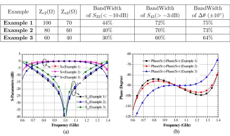
Table 1. The design parameters of Examples 1,2, and 3.
Example Ze2(Ω) Zo2(Ω)
BandWidth ofS33(<−10 dB)
BandWidth of S43(>−3 dB)
BandWidth of Δθ(±10◦)
Example 1 100 70 44% 72% 75%
Example 2 80 60 40% 70% 73%
Example 3 60 40 30% 60% 64%
0.6 0.7 0.8 0.9 1.0 1.1 1.2 1.3 1.4 -40 -35 -30 -25 -20 -15 -10 -5 0 5 (a) S43(Example 1) S43(Example 2) S43(Example 3)
S -P ara m eters (d B ) Frequency (GHz)
S33(Example 1) S33(Example 2) S33(Example 3)
0.6 0.7 0.8 0.9 1.0 1.1 1.2 1.3 1.4 -120 -110 -100 -90 -80 -70 -60 (b) P h as e (D eg ree) Frequency (GHz) Phase(S21)-Phase(S43) (Example 1) Phase(S21)-Phase(S43) (Example 2) Phase(S21)-Phase(S43) (Example 3)
Figure 3. The calculated results of Example 1, 2, and 3: (a) Scattering Parameters; (b) Phase information.
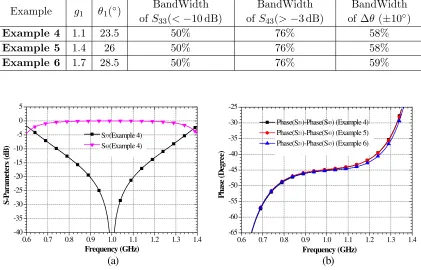
3.3. The Selection of g1 and θ1
which are based on the lossless coupled-line model. Note that the circuit parameters of the reference line are the same, only scattering parameters of Example 4 are plotted in Figure 4. From Table 2 and Figure 4, it can be observed that with different g1 and θ1, the bandwidth of the phase shifter is almost the same, indicating that the selection of g1 and θ1 has little influence on the bandwidth of the phase shifter.
Table 2. The design parameters of Examples 4,5, and 6.
Example g1 θ1(◦)
BandWidth ofS33(<−10 dB)
BandWidth of S43(>−3 dB)
BandWidth of Δθ(±10◦)
Example 4 1.1 23.5 50% 76% 58%
Example 5 1.4 26 50% 76% 58%
Example 6 1.7 28.5 50% 76% 59%
0.6 0.7 0.8 0.9 1.0 1.1 1.2 1.3 1.4 -40
-35 -30 -25 -20 -15 -10 -5 0 5
S33(Example 4) S43(Example 4)
S
-P
ara
m
eters (d
B
)
Frequency (GHz)
0.6 0.7 0.8 0.9 1.0 1.1 1.2 1.3 1.4 -65
-60 -55 -50 -45 -40 -35 -30 -25
P
h
as
e (D
eg
ree)
Frequency (GHz) Phase(S21)-Phase(S43) (Example 4) Phase(S21)-Phase(S43) (Example 5) Phase(S21)-Phase(S43) (Example 6)
(a) (b)
Figure 4. The calculated results of Examples 4, 5, and 6: (a) Scattering Parameters; (b) Phase information.
4. SIMULATED AND MEASURED RESULTS
The analytical solutions and parameter analyses have been theoretically explained in Sections 2 and 3. In order to verify this proposed wideband phase shifter experimentally, two examples (Example Aand
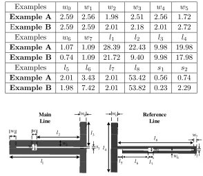
Example B) are fabricated on a radio frequency substrate F4B with a relatively dielectric constant of 2.65 and a thickness of 1 mm. These two examples are designed by using microstrip realization technology with complete ground plane in the bottom layer, and the operating frequency is chosen at 1 GHz. Tables 3 and 4 list the initial electrical parameters and the corresponding physical circuit parameters, respectively. The above-layer circuit trace layout of the proposed circuit with defined dimension parameters is shown in Figure 5. Note that all port impedances are 50 Ω in this paper.
Table 3. The circuit parameters of Examples A and B.
Examples Ze1(Ω) Zo1(Ω) θ1(◦) Ze2(Ω) Zo2(Ω) θ2(◦)
Example A 60 41.67 50 100 67 90
Table 4. The physical circuit parameters (unit: mm) of Examples A and B.
Examples w0 w1 w2 w3 w4 w5
Example A 2.59 2.56 1.98 2.51 2.56 1.72 Example B 2.59 2.59 2.01 2.18 2.01 2.72
Examples w6 w7 l1 l2 l3 l4
Example A 1.07 1.09 28.39 22.43 9.98 19.98
Example B 0.74 1.09 21.72 9.40 9.98 17.98
Examples l5 l6 l7 l8 s1 s2
Example A 2.01 3.43 2.01 53.42 0.56 0.74
Example B 1.98 7.42 2.01 53.82 0.23 2.29
Main Line
Reference Line
w0 w0
w1 w2
w3
w4
w5 w6
w7
l1
l2 l3
l4
l5 l6 l7
s1
s2 l8
Figure 5. The layout of the proposed phase shifter.
-30 -25 -20 -15 -10 -5 0 5
S
-P
ara
m
eters (d
B
)
Frequency (GHz) S11 S21 S33 S43
(a)
0.6 0.7 0.8 0.9 1.0 1.1 1.2 1.3 1.4 -200
-150 -100 -50 0 50 100
(b)
P
h
as
e (D
eg
ree)
Frequency (GHz) Phase(S21) Phase(S43) Phase(S21)-Phase(S43)
0.6 0.7 0.8 0.9 1.0 1.1 1.2 1.3 1.4
Figure 6. The calculated results of Example A: (a) Scattering Parameters; (b) Phase information.
The phase difference of Example A (Example B) is −90◦ (−60◦). The definition of the circuit parameters ofExample Bis the same as that of Example Alisted in Table 3 and Table 4. Figure 6(a) and Figure 7(a) plot the calculated scattering parameters of the two examples, while Figure 6(b) and Figure 7(b) present the phase information. Figures 6 and 7 show that all ports are matched ideally. The 10-dB return loss fractional bandwidth is almost 44% (from 0.78 GHz to 1.22 GHz) for Example A
0.6 0.7 0.8 0.9 1.0 1.1 1.2 1.3 1.4 -30
-25 -20 -15 -10 -5 0 5
S
-P
ara
m
eters (d
B
)
Frequency (GHz) S11 S21 S33 S43
(a)
0.6 0.7 0.8 0.9 1.0 1.1 1.2 1.3 1.4 -100
-80 -60 -40 -20 0 20 40 60
(b) Phase(S21) Phase(S43) Phase(S21)-Phase(S43)
P
h
a
se (D
eg
ree)
Frequency (GHz)
Figure 7. The calculated results of Example B: (a) Scattering Parameters; (b) Phase information.
(a) (b)
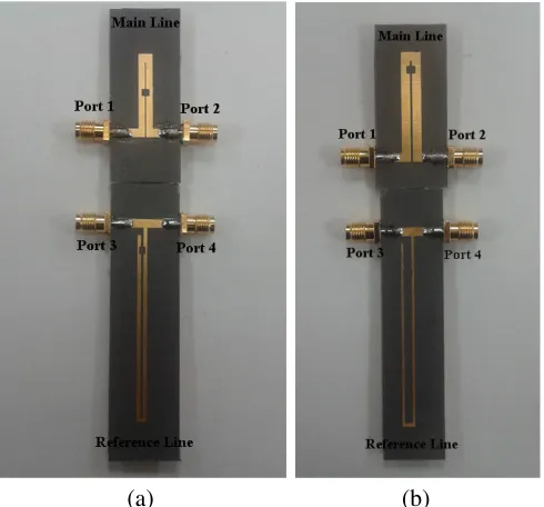
Figure 8. Top view of the fabricated microstrip phase shifter: (a)Example A; (b) Example B.
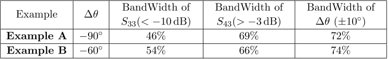
Photographs of the final fabricated circuit (Examples A and B) are shown in Figure 8. The measured results using Agilent N5230C Vector Network Analyzer are plotted in Figures 9 and 10. The 10-dB return loss fractional bandwidth is almost 46% (from 0.81 GHz to 1.27 GHz) for the Example Aand 54% (from 0.73 GHz to 1.27 GHz) for the Example B. However, the calculated phase difference fractional bandwidth between the main line and the reference is almost 72% (from 0.66 GHz to 1.38 GHz) forExample Aand 74% (from 0.65 GHz to 1.39 GHz) forExample B based on the±10◦ phase error. To see the measured results more clearly, Table 5 lists the bandwidths of S33, S43, and Δθ. Small performance degradation can be due to the conductor loss, dielectric loss, or measurement errors and so on. In general, it can be concluded that there is a good agreement between the calculated and measured results including magnitude and phase information.
Based on the investigation on the proposed circuit, a simple design procedure can be summarized as follows.
0.6 0.7 0.8 0.9 1.0 1.1 1.2 1.3 1.4 -30 -25 -20 -15 -10 -5 0 5 S -P ara m eters (d B ) Frequency (GHz) S11 S21 S33 S43
0.6 0.7 0.8 0.9 1.0 1.1 1.2 1.3 1.4 -200 -150 -100 -50 0 50 100
Phase(S21) Phase(S43) Phase(S21)-Phase(S43)
P h as e (D eg ree) Frequency (GHz) (a) (b)
Figure 9. The measured results of Example A: (a) Scattering Parameters; (b) Phase information.
0.6 0.7 0.8 0.9 1.0 1.1 1.2 1.3 -40 -35 -30 -25 -20 -15 -10 -5 0 5 S -P ara m eters (d B ) Frequency (GHz) S11 S21 S33 S43 (a)
0.6 0.7 0.8 0.9 1.0 1.1 1.2 1.3 1.4 -160 -120 -80 -40 0 40 (b)
Phase(S21) Phase(S43) Phase(S21)-Phase(S43)
P h as e (D eg ree) Frequency (GHz)
Figure 10. The measured results of Example B: (a) Scattering Parameters; (b) Phase information.
Table 5. The measured results of Examples Aand B.
Example Δθ BandWidth of
S33(<−10 dB)
BandWidth of S43(>−3 dB)
BandWidth of Δθ (±10◦)
Example A −90◦ 46% 69% 72%
Example B −60◦ 54% 66% 74%
2) Determine the proper g1 and the electrical length θ1 of the main line according to the Equations (6) and (12) when the phase difference is fixed. Then calculate the impedanceZe1,Zo1.
3) Choose the appropriate impedance of the reference line.
4) Convert all the electrical parameters to the physical dimensions, and calculate the total scattering parameters and the available bandwidth by using lossless transmission lines.
5. CONCLUSION
In this paper, a modified coupled-line Schiffman phase shifter with short reference line is proposed. The design theories, including analytical equations, scattering parameters and phase difference, are provided. For observation of the bandwidth of the scattering parameters and phase difference, six examples are discussed. For experimental demonstration, two microstrip phase shifters are designed, fabricated, and measured. Good agreements can be observed for the calculated and measured results. Due to easy realization of the proposed circuit structure, it is expected that this phase shifter will be used in various microwave components and systems.
ACKNOWLEDGMENT
This work was supported in part by the National Key Basic Research Program of China (973 Program) (No. 2014CB339900), National Science and Technology Major Project (No. 2012ZX03001001-002), National Natural Science Foundation of China for the Major Equipment Development (No. 61327806), Open Project of the State Key Laboratory of Millimeter Waves (Grant No. K201316), and Specialized Research Fund for the Doctor Program of Higher Education (No. 20120005120006).
REFERENCES
1. Hayashi, H., D. A. Hitko, and C. G. Sodini, “Four-element planar Butler matrix using half-wavelength open stubs,” IEEE Microwave Compon. Lett., Vol. 12, No. 3, 73–75, 2002.
2. Gruszczynski, S., K. Wincza, and K. Sachse, “Broadband 4×4 Butler matrices utilizing tapered-coupled-line directional couplers,”Microw., Radar Remote Sens. Symp., MRRS-Proc., 77–81, Kiev, Ukraine, Aug. 2011.
3. Wu, Y., Q. Liu, J.-Y. Shen, and Y. Liu, “A novel wide-band hybrid coupler using coupled-line power divider and improved coupled-line phase shifter,” Journal of Electromagnetic Waves and Applications, Vol. 27, No. 3, 374–384, 2013.
4. Opp, F. L. and W. F. Hoffman, “Design of digital loaded-line phase-shift networks for microwave thin-film applications,” IEEE Trans. Microwave Theory Tech., Vol. 16, No. 7, 462–468, Jul. 1968. 5. Yahara, T., “A note on designing digital diode-loaded-line phase shifters,”IEEE Trans. Microwave
Theory Tech., Vol. 20, No. 10, 703–704, Oct. 1972.
6. Alan Davis, W., “Design equations and bandwidth of loaded-line phase shifters,” IEEE Trans. Microwave Theory Tech., Vol. 22, No. 5, 561–563, May 1974.
7. Atwater, H. A., “Circuit design of the loaded-line phase shifter,” IEEE Trans. Microwave Theory Tech., Vol. 33, No. 7, 626–634, Jul. 1985.
8. Schiffman, B. M., “A new class of broad-band microwave 90-degree phase shifters,” IRE Trans. Microwave Theory Tech., Vol. 6, No. 2, 232–237, Apr. 1958.
9. Quirarte, J. L. R. and J. P. Starski, “Novel Schiffman phase shifters,” IEEE Trans. Microwave Theory Tech., Vol. 41, No. 1, 9–14, Jan. 1993.
10. Schiffman, B. M., “Multisection microwave phase-shift network (Correspondence),” IEEE Trans. Microwave Theory Tech., Vol. 14, No. 4, 209, 1966.
11. Quirarte, J. L. R. and J. P. Starski, “Synthesis of Schiffman phase shifters,”IEEE Trans. Microwave Theory Tech., Vol. 39, No. 11, 1885–1889, Nov. 1991.
12. Free, C. E. and C. S. Aitchison, “Improved analysis and design of coupled-line phase shifters,” IEEE Trans. Microwave Theory Tech., Vol. 43, No. 9, 2126–2131, Sep. 1995.
13. Leong, Y. C. and S. Weinreb, “Novel technique of phase velocity equalization for microstrip coupled-line phase shifters,”IEEE MTT S Int. Microwave Symp. Dig., Vol. 3, 1453–1456, Boston, MA, USA, 2000.
15. Oraizi, H. and A. Shamsafar, “Optimum design of modified Schiffman multi-section wide band differential phase shifter with impedance matching,” Progress In Electromagnetics Research C, Vol. 29, 1–16, 2012.
16. Minnaar, F. V., J. C. Coetzee, and J. Joubert, “A novel ultrawideband microwave differential phase shifter,”IEEE Trans. Microwave Theory Tech., Vol. 45, No. 8, 1249–1252, Aug. 1997.
17. Sung, G. J., R. Kasim, J. Y. Ryu, and B. Kim, “Broadband 180◦ bit X-band phase shifter using parallel-coupled lines,” 35th Eur. Microwave Conf. 2005 Conf. Proc., Vol. 3, 2043–2045, Paris, France, 2005.
18. Zheng, S. Y., W. S. Chan, and K. F. Man, “Broadband phase shifter using loaded transmission line,” IEEE Microwave Compon. Lett., Vol. 20, No. 9, 498–500, Sep. 2010.
19. Yeung, S. H., Z. Mei, T. K. Sarkar, and M. Salazar-Palma, “Design and testing of a single-layer microstrip ultrawideband 90◦ differential phase shifter,” IEEE Microwave Compon. Lett., Vol. 23, No. 3, 122–124, Mar. 2013.
20. Geogre, G. I., I. Zysman, and A. K. Johnson, “Coupled transmission line networks in an inhomogeneous dielectric medium,” IEEE Trans. Microwave Theory Tech., Vol. 17, No. 10, 753– 759, Oct. 1969.