ANALYSIS AND DESIGN OF AN ULTRA-THIN METAMATERIAL ABSORBER
R. F. Huang, Z. W. Li, L. B. Kong, L. Liu, and S. Matitsine
Temasek Laboratories
National University of Singapore Singapore 117411, Singapore
Abstract—This paper presents a class of ultra-thin metamaterial absorbers, which consists of periodic microstrip lines on top of a planar lossy substrate backed by a conducting metallic plate. A highly efficient full-wave analysis method was developed to solve the electromagnetic response of the absorbers. The influence of electromagnetic properties of the substrate and physical dimensions of the microstrip lines were analyzed. Genetic algorithm was used to optimize the absorption bandwidth of the absorbers. Effective permeability and permittivity of the absorbers were retrieved to shed a new light on the absorption mechanism of the absorbers and to explain their ultimate bandwidth limit. It was found that the ultimate bandwidth limit of the metamaterial absorbers is the same as that of normal absorbers.
1. INTRODUCTION
In recent years, metamaterials have drawn a great deal of attention in the scientific community. Due to their exotic electromagnetic properties resultant from the artificially tailored electric [1] and magnetic [2] responses, metamaterials have been used to produce negative refraction [3], subwavelenth image resolution [4, 5], and cloaking effects [6–8]. From the effective medium point of view, the exotic electromagnetic properties of metamaterials are due to the specifically tailored effective relative permeability (μ=μ−jμ) and relative permittivity (= −j) [9]. In much of the research work on metamaterials, electric and magnetic loss is avoided. Actually, the loss of metamaterials can be utilized to absorb electromagnetic
waves [10, 11]. In [10], design of an absorbing metamaterial with near unity absorbance at a single frequency was presented. The perfect absorbing effect was achieved by manipulating the effectiveμ andof the metamaterial to match each other at a certain frequency and thus to match the wave impedance to the free space value at that frequency. Theoretical work has revealed that short strip pairs (SSPs) [12– 14] show strong magnetic responses, just as split-ring resonators (SRRs) [2], at the free space wavelengths much larger than the distance between the two short strips. SSPs have been applied to the design of metamaterials at the frequencies of microwave and even higher. Compared with SRRs, SSPs have the advantages of easy fabrication and simple experimental characterization. For periodic SSPs, it has been analytically and experimentally demonstrated that if the width, which is in the direction perpendicular to the incident E field, of the short strips increases, the resonant frequency of the SSPs will decrease slightly [14]. In the extreme case, increasing the width of the two-dimensional periodic short strips until adjacent short strips connect in the direction of width expansion will result in one-dimensional periodic microstrip lines. Thus there is actually no difference in the underlying mechanism between SSPs and microstrip line pairs. However, as shown in Section 2 and Section 4, reducing the two dimensional periodic SSPs into one-dimensional periodic microstrip line pairs results in great reduction in analysis complexity.
permeability and permittivity of the microstrip line metamaterial absorbers are retrieved, which shed a new light on the absorption mechanism of the metamaterial absorbers. The ultimate bandwidth limit of the metamaterial absorbers is explained in Section 6. In Section 7, a brief conclusion is drawn.
2. UNIFORM MICROSTRIP LINE METAMATERIAL ABSORBER
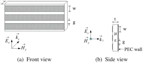
The uniform microstrip line metamaterial absorber is illustrated in Fig. 1. For simplicity, only normal incidence is considered. The polarization direction of the electric fields is perpendicular to the microstrip lines. The microstrip lines and the backing metallic wall are assumed to be perfectly electric conductors (PEC). With the periodic characteristic of the structure taken into account, the computational model of the original structure is shown in Fig. 2. It can be seen that the computational model actually is an ideal short-ended parallel plate discontinuous waveguide. Due to the uniformity of the structure in the
y direction, analysis can be simply performed on the cross section of
(b) Side view (a) Front view
Figure 1. The metamaterial absorber under consideration.
(b) Side view (a) Front view
1 A x
2 A x
2 B x
1 B x A
d dB
x
z
0
z z
1 A x
2 A x
2 B x
1 B x A
d dB
x
z
0
z z
(a) Case 1 (b) Case 2
= =
section A section B section A section B
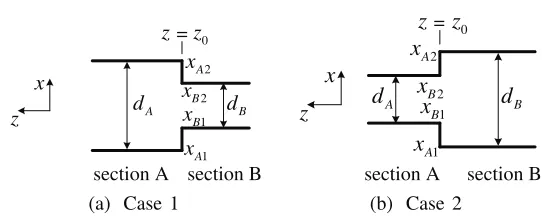
Figure 3. Parallel plate discontinuities under consideration.
the structure in thexz plane.
Mode matching method [16–20] has been widely used to efficiently solve waveguide discontinuity problems. For the parallel plate discontinuous waveguides, usually there are two types of discontinuities, as shown in Fig. 3(a) and Fig. 3(b) respectively. For illustration of the principle of the mode matching method when applied to the parallel plate discontinuous waveguides, the discontinuity shown in Fig. 3(a) is considered first. The structure has two sections, i.e., section A and section B, separated by a discontinuity interface located at z = z0. Since the structure is uniform along the y
direction, only transverse magnetic (TM) modes are excited on the discontinuity interface for the transverse electric and magnetic (TEM) wave excitation. The two kinds of discontinuities can be analyzed based on the mode matching method by following the similar analysis procedure presented in [17]. The equations as below can be obtained for the discontinuity in Fig. 3(a):
L1n[CAn+CAnΓAn] = ∞
m=0
R1mn[CBmΓBme−γBmLB+CBmeγBmLB] (1)
L2m jωB
γBm
CBmΓBme−γBmLB−CBmeγBmLB
=
∞
n=0
jωA γA
R2mn[CAnΓAn−CAn] (2)
whereCAn,CAnΓAn,CBm, andCBmΓBmare the unknown coefficients to be determined, which represent the magnitudes of the nth forward (−z direction) traveling mode in section A, the nth backward (+z
respectively:
L1n =
xA2
xA1
cos2
nπ
dA(x−xA1)
dx=
dA, (n= 0) 0.5dA, (n= 0) (3)
R1mn=
xB2
xB1
cos
mπ
dB(x−xB1)
cos
nπ
dA(x−xA1)
dx = ⎧ ⎪ ⎪ ⎪ ⎪ ⎪ ⎪ ⎪ ⎪ ⎪ ⎪ ⎪ ⎪ ⎪ ⎪ ⎪ ⎪ ⎪ ⎪ ⎪ ⎪ ⎨ ⎪ ⎪ ⎪ ⎪ ⎪ ⎪ ⎪ ⎪ ⎪ ⎪ ⎪ ⎪ ⎪ ⎪ ⎪ ⎪ ⎪ ⎪ ⎪ ⎪ ⎩
dB, (m= 0, n= 0),
0, (m= 0, n= 0),
1 2
1
mπ dB +
nπ dA
sin
mπ dB +
nπ dA x− mπ dBxB1+
nπ dAxA1
+mπ 1
dB −
nπ dA
sin
mπ dB −
nπ dA x− mπ dB
xB1−
nπ dA
xA1
x
B2 xB1,
mπ dB =
nπ dA, n= 0
, 1 2 1 mπ dB +
nπ dA
sin
mπ dB +
nπ dA x− mπ dB xB1+
nπ
dAxA1 xB2 xB1
+1
2dB1cos
mπ
dB (xA1−xB1)
,
mπ dB =
nπ dA, n= 0
(4)
f(x)x2x1 =f(x2)−f(x1) (5)
L2m =
xB2
xB1
cos2
mπ
dB(x−xB1)
dx=
dB, (m= 0)
0.5dB, (m= 0) (6)
R2mn=R1mn=
xB2
xB1
cos
mπ dB
(x−xB1)
cos
nπ dA
(x−xA1)
dx (7)
In Fig. 3(b), section B has a larger cross section than section A. The resultant equations obtained can be expressed as below:
L1njωA γAn
[CAnΓAn−CAn]
=
∞
m=0
jωB γBm R
1mn
CBmΓBme−γBmLB−C
BmeγBmLB
(8)
L2mCBmΓBme−γBmLB+C
BmeγBmLBm
=
∞
n=0
where
L1n = L1n=
dA, (n= 0)
0.5dA, (n= 0) (10)
R1mn = xA2
xA1
cos
mπ
dB (x−xB1)
cos
nπ
dA (x−xA1)
dx (11)
L2m = L2m =
dB, (m= 0)
0.5dB, (m= 0) (12)
R2mn = R1mn (13)
It is noted that in the first section the given incident TEM wave is the only forward traveling mode. When the last section extends into infinity, there will be no backward traveling waves. In other words, the reflection coefficients of all the modes in the last section are zeros in that case. When the last section is short-ended, the reflection coefficients of all the modes in the last section are −1. With the boundary conditions of the first section and the last section taken into account, the number of the unknown variables is equal to the number of the equations obtained. The equations can be written into the following matrix form from which the unknown coefficients can be easily solved:
⎡ ⎢ ⎣
X X 0 · · · 0 0 X X 0 · · ·
· · · ·
0 · · · 0 X X
⎤ ⎥ ⎦
×[Γ1,0C1,0· · ·Γ1,m1C1,m1|C2,0· · ·C2,m2|Γ2,0C2,0· · ·Γ2,m2|· · ·|Csn,0· · ·Csn,msn]T =[x0 · · · | 0 · · · 0 0 · · · 0|0 · · · 0]T (14)
In (14), the superscriptT means transposition of the matrix. The first and only nonzero element in the right hand side of (14) is due to the incident TEM wave, as can be seen from (1) and (8).
8 8.5 9 9.5 10 -30
-20 -10 0
Frequency (GHz)
Reflection (dB)
8 8.5 9 9.5 10
-200 -100 0 100 200
Frequency (GHz)
Phase (deg)
(a) (b)
Figure 4. Reflection coefficients of a uniform microstrip line metamaterial absorber (solid lines: mode matching method; circles: HFSS).
when a normal PC (Intel Core2 Duo CPU E6750@2.66 GHz, 3.25 GB of Random Access Memory) is used.
Figure 5. Typical reflection coefficients of an absorber.
3. OPTIMIZATION OF THE METAMATERIAL
ABSORBER BY USING THE GENETIC ALGORITHM
The electromagnetic response of the metamaterial absorber is determined by many factors, including the width of the microstrip lines, the gap between the microstrip lines, the thickness of the substrate, and the permeability and permittivity of the substrate. Thus optimization of the performance of the microstrip line metamaterial absorber is a high-dimensional optimization problem.
can be used in many different areas. The only connection between the genetic algorithm and the specific problem to be optimized is the fitness function. The returned value of the fitness function represents the goodness of the solution. The input parameters to be optimized are coded into a finite-length string consisting of real numbers. The coded parameters are represented by genes in the chromosome. The genetic algorithm operates on the genes rather than the parameters themselves, and thus is independent on the actual solution space. During the optimization process, the genetic algorithm iteratively evolves the genes by performing the selection, crossover and mutation operation to maximize the returned value of the fitness function.
For optimization of the metamaterial absorber, the appropriate fitness function has to be defined first. The reflection coefficients of the absorbers in the frequency range from f1 and f2 can be typically illustrated in Fig. 5. In the frequency range from f1 and f2, the reflection coefficients are below the required absorption limit, e.g., −10 dB. The main objective of the optimization is to maximize the −10 dB absorption bandwidth around the center frequency f0. The bandwidth can be written as follows:
Bandwidth = 2×min(f2−f0, f0−f1) (15) There may be some cases where the absorption bandwidths are the same while the absorption strengths, which are depicted as Area 1 in Fig. 5, are different. With the absorption strength taken into account, the fitness function can be expressed as follows:
fitness = Bandwidth + weight×Area 1,(Bandwidth>0) (16) where weight is a small number such that the returned value of the fitness function is mostly dependent on the bandwidth.
The fitness function defined in (16) is valid as long as the bandwidth is larger than zero. However, there may be many cases where the reflection coefficients are all above the absorption limit, and thus the bandwidth is zero. In those cases the fitness function can be defined in terms of Area 2 in Fig. 5 as follows:
fit individuals, negative returned value of the fitness function is thus allowed.
The highly efficient mode matching method presented in the last section makes it practical to optimize the metamaterial absorber by using the genetic algorithm. During the optimization process, the thickness of the microstrip lines is set to be 0.02 mm which is in the typical range of the thickness of metallic coatings. The influence of the variation of that thickness is numerically analyzed and found to be negligible when the thickness is in the range from 0.01 mm to 0.03 mm. Furthermore, the microstrip lines are assumed to be perfectly electric conductors (PEC), which are found numerically to be very good approximation to coppers which are usually used in metallic coatings. As previously mentioned, the performance of the metamaterial absorber is determined by the width (w) of the microstrip lines, the gap (g) between the microstrip lines, the thickness of the substrate (t), and the relative permeability (μ = μ(1−jtanδμ)) and the relative
permittivity (=(1−jtanδ)) of the substrate. Those parameters are to be determined by using the genetic algorithm. The metamaterial absorber consisting of dielectric substrate is considered first. The searching boundaries of the parameters to be determined and the number of bits of the binary coding are shown in Table 1.
In this example, the thickness of the substrate is chosen to be 0.5 mm, i.e., around 1/66λwhen the center frequency of the absorption waveband is 9 GHz. The lower bound of g shown in Table 1 is mainly determined by the manufacturing precision. The other searching bounds are determined to cover the mathematically possible and physically realizable solutions. For easy and precise manufacturing of the microstrip lines, the binary coding bits of w and g are chosen to be 5 and 3 respectively such that all the possible w and g are of integer times of 0.1 mm. The coding bits of the other parameters are set to be 16 such that those parameters can vary almost continuously in their searching bounds. The optimized parameters of the metamaterial absorber consisting of a dielectric substrate are shown in the first row in Table 2.
Table 1. Boundaries of the parameters to be determined.
Parameters w(mm) g (mm) tanδ
Lower bound 1.0 0.4 1 0.01
Upper bound 7.2 1.8 20 1
Table 2. The results of the optimized uniform microstrip line metamaterial absorbers (t= 0.5 mm).
Searching bounds ofμ w
(mm)
g
(mm)
tanδ tanδμ BW
(GHz)
μ=1,tanδμ=0 5.8 0.4 6.15 0.103 0 0.53
μ=1.5, 0.01≤tanδ
μ≤1 3.4 0.4 10.57 0.135 0.025 0.79
μ=2.0, 0.01≤tanδ
μ≤1 6.6 0.4 2.13 0.109 0.124 1.10
μ=2.5, 0.01≤tanδμ≤1 2.8 0.4 8.33 0.090 0.187 1.39
Optimization of the metamaterial absorber consisting of a magnetic substrate can be similarly carried out by specifying the searching boundaries ofμand keeping the searching boundaries of the other parameters shown in Table 1 unchanged. The optimized results for three different searching boundaries of μ are shown in the last three rows in Table 2. From Table 2, it can be seen that the optimized bandwidth is approximately proportional toμ. Further discussions on the influence of the permeability and the thickness of the substrate on the bandwidth of the metamaterial absorber are presented in Section 6. The reflection coefficients of the optimized absorbers in Table 2 are shown in Fig. 6.
8 8.5 9 9.5 10
-25 -20 -15 -10 -5 0
Frequency (GHz)
Reflection (dB)
4. NONUNIFORM MICROSTRIP LINE METAMATERIAL ABSORBER
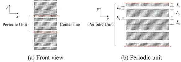
In the last section, uniform microstrip line metamaterial absorber was optimized by combining the highly efficient mode matching method and the genetic algorithm. From the optimized results, it can be seen that a strong absorption peak occurs at the center frequency of the absorption waveband. From the equivalent circuit point of view, the microstrip line pair constructed from a mirostrip line and its image with respect to the backing metallic wall can be seen as parallel of a lossy capacitor and an inductor which is also lossy for a magnetic substrate. The center frequency corresponds to the resonant frequency of the equivalent LC circuit. The parameters of the equivalent capacitor and the equivalent inductor are determined by both the electromagnetic properties of the substrate and the physical dimensions of the microstrip line pair. Thus, when nonuniform microstrip lines are used in the periodic unit as shown in Fig. 7, the equivalent circuit of the microstrip line pairs cannot be represented by a single parallel LC circuit anymore. The nonuniform microstrip lines lead to multiple parallel LC circuits with different resonant frequencies in the equivalent circuit. Thus, the absorption bandwidth of the absorber may be broadened by proper design of the nonuniform microstrip lines. However, the equivalent circuit is only good for qualitative analysis, even for very simple structures [13, 14, 26, 27]. To accurately determine the performance of the nonuniform microstrip line metamaterial absorber, we have to resort to the numerical methods.
The only difference between the computational models of the uniform microstrip line metamaterial absorber and the nonuniform microstrip line metamaterial absorber is that there are two gaps in the second section, i.e., the section consisting of the metallic microstrip
(b) Periodic unit (a) Front view
lines, in the latter computational model, as shown in Fig. 8. There are two types of waveguide discontinuity interfaces in the structure, as shown in Fig. 9(a) and Fig. 9(b) respectively. For the discontinuity interface shown in Fig. 9(a), the following equations can be obtained by following the similar analysis procedures in the mode matching method [17]:
L1n[CAn+CAnΓAn] = ∞
m=0
Rpmn[CpmΓpme−γpmLp+C
pmeγpmLp]
+
∞
m=0
Rqmn[CqmΓqme−γqmLp+C
qmeγqmLq] (18) L2m
jωy γym
[CymΓyme−γymLy−C
ymeγymLy]
=
∞
n=0
jωA γAn
Rymn[CAnΓAn−CAn], (y=p orq) (19)
where the terms with the subscriptp and q are related to waveguide
p and waveguide q shown in Fig. 9(a) respectively, L1n is the same as
expressed in (3), and
Rymn =
xy2
xy1
cos
mπ xy2−xy1
(x−xy1)
cos
nπ
dA(x−xA1)
dx,
(y =p or q) (20)
L2m =
xy2
xy1
cos2
mπ xy2−xy1
(x−xy1)
dx, (y =p or q) (21) For the discontinuity interface shown in Fig. 9(b), the following
wall
(b) Side view (a) Front view
1 A x 2 A x 2 q x 1 q x A d q d x z 0 z z 2 p x 1 p x dp
x z 1 B x 2 B x 2 q x 1 q x q d 0 z z 2 p x 1 p x p d B d
(a) Case 1 (b) Case 2
= =
section B
section A section A section B
Figure 9. Computational model of the nonuniform microstrip line metamaterial absorber.
equations can be obtained:
L1njωy γyn
[CynΓyn−Cyn]
= ∞ m=0 jωB γBm
R1mn[CBmΓBme−γBmLB−CBmeγBmLB],(y=p orq) (22) L2m[CBmΓBme−γBmLB +CBmeγBmLB]
=
∞
n=0
Rpmn[CpnΓpn+Cpn] + ∞
n=0
Rqmn[CqnΓqn+Cqn] (23)
where
L1n= xy2
xy1
cos2
nπ xy2−xy1
(x−xy1)
dx, (y=porq) (24)
R1mn =Rymn= xy2
xy1
cos
mπ dB
(x−xB1)
×cos
nπ xy2−xy1
(x−xy1)
dx, (y=por q) (25)
L2m = xB2
xB1
cos2
nπ xB2−xB1
(x−xB1)
dx (26)
8 8.5 9 9.5 10 -20
-15 -10 -5 0
Frequency (GHz)
Reflection (dB)
MM microstrip line HFSS microstrip line HFSS rectangular patch
Figure 10. Reflection coefficients of an optimized 0.8 mm thick dielectric substrate metamaterial absorber.
Table 3. Optimized results of a 0.8 mm thick nonuniform microstrip line metamaterial absorber.
μ L1
(mm)
L2
(mm)
L3
(mm)
L4
(mm)
L5
(mm) BW (GHz)
1.0 5.44(1−j0.1) 3.1 0.4 5.5 1.0 2.8 1.39
To maximize the−10 dB absorption bandwidth of the nonuniform microstrip line metamaterial absorber, the genetic algorithm can be used to optimize the widths of the microstrip lines and the gaps between the microstrip lines in the periodic unit, and the electromagnetic properties of the substrate. As an example, the reflection coefficients of an optimized 0.8 mm thick dielectric substrate microstrip line metamaterial absorber are shown in Fig. 10. The optimized parameters of the absorber are shown in Table 3. Based on these optimized parameters, the commercial software HFSS is also used to simulate the reflection coefficients of the metamaterial absorber. From Fig. 10, very good agreement between the results of the mode matching method (shown as circles) and HFSS (shown as a solid line) can be observed. The great increase of absorption bandwidth by using nonuniform microstrip lines can be easily observed by comparison of Fig. 10 and Fig. 4 which shows the reflection coefficients of an optimized uniform microstrip line metamaterial absorber with the same thickness of substrate and the same center frequency.
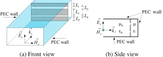
used. The rectangular patch metamaterial absorber is constructed by applying the one-dimensional periodic pattern of the microstrip line metamaterial absorber in both the x and the y directions. Based on the parameters in Table 3, the reflection coefficients of the rectangular patch metamaterial absorber are calculated by using HFSS. The simulation results are shown in Fig. 10 as ‘+’. It can be seen from Fig. 10 that the reflection coefficients of the two types of metamaterial are very similar. Thus the optimized microstrip line metamaterial absorber is a good starting point for the design of the rectangular patch metamaterial absorber. It is noted that the absorption peaks of the rectangular patch metamaterial absorber shifts slightly toward higher frequencies. The reason has been previously mentioned and explained in detail in [14].
Figure 11. Front view of the rectangular patch metamaterial absorber.
5. EFFECTIVE PERMEABILITY AND PERMITTIVITY OF THE METAMATERIAL ABSORBER
For better characterization of metamaterials, researches have been done to retrieve their effective permeability and permittivity [9, 26, 27]. A “foolproof” approach for unique retrieval of the effective μand of metamaterials by enforcing causality is presented in [27]. The Kramers-Kronig relation between the real part (α) and the imaginary part (β) of the effective complex propagation constant (γ =α+jβ) in the sample is used to reconstruct β in terms of α. Since α is well determined, and β contains an unknown integer m, the reconstructed β from the Kramers-Kronig relation provides a guideline for the correct choice of
m. No initial guess of m is required.
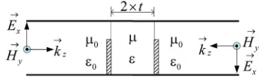
the mode matching method presented above, the effective μand can be retrieved by using the approach in [29]. It is true that the peri-odic unit of the microstrip line metamaterial absorber, especially the nonuniform microstrip line metamaterial absorber, may not be much smaller than the wavelength of the upper frequency in the waveband of interest. But it is not difficult to find that as long as all the high order modes cannot propagate, only TEM wave will exist somewhere away from the metamaterial absorber. In that sense, metamaterial ab-sorber can be totally equivalent to a homogenous slab abab-sorber with the permeability and permittivity of the slab being the effective values retrieved.
Figure 12. Equivalent computational model of the uniform microstrip line metamaterial absorber.
As an example, the uniform microstrip line metamaterial absorber shown in the first row in Table 2 is considered. The retrieved effective
μandof the metamaterial absorber are shown in Fig. 13 as the lines without the circle markers.
For simple validation of the retrieved effective μ and , the reflection coefficients of the metamaterial absorber are obtained by using the following well known equation for normal single-layered metal-backed slab absorbers [30]:
Γ = Zin−1
Zin+ 1
(27)
where
Zin=μ/tanh(jω√μ√μ00t) (28) and t is the thickness of the substrate. The reflection coefficients are also calculated based on the computational model in Fig. 2 by using the mode matching method. The results of the two methods are shown in Fig. 14. Very good agreement between the results of the two methods can be observed.
response is due to the resonant effect of the metallic structure. From Fig. 12, it can be clearly seen that the metallic microstrip line and its image effectively form a microstrip line pair, which acts as an effective macro magnetic atom to produce the magnetic response [13, 14]. At very low frequencies, since the resonant effect of the microstrip line pair disappears, the magnetic response is dependent on the substrate only. Thus the effective relative permeability shown in Fig. 13(a) tends to be the relative permeability of the substrate, i.e., 1, at very low frequencies. If the relative permeability of the substrate is assumed to be 1.5(1 − j0.1) and the relative permittivity and the physical dimensions shown in the first row in Table 2 remain unchanged, the retrieved effective μandof the uniform microstrip line metamaterial absorber are shown in Fig. 13 as the lines with the circle markers. In this case, it can be seen that the effective relative permeability at very low frequencies approaches 1.5(1−j0.1).
From Fig. 14(b), it can be seen that the effective permittivity of the absorber at very low frequencies are much higher than the permittivity of the substrate. The enhancement of the permittivity is due to the large capacitance between the metallic microstrip lines. Since the electric response of the structure at very low frequencies are independent on the permeability of the substrate, the effective permittivities of the two metamaterial absorbers with different permeabilities of the substrate are the same at very low frequencies, as can be seen from Fig. 13. Around the resonant frequency, the antiresonant frequency dependence of the effective permittivity is observed. According to [31, 32], that phenomena is due to the finite spatial periodicity of the metamaterial.
2 4 6 8 10 12
-2 0 2 4 6
Frequency (GHz)
Effective
2 4 6 8 10 12
-50 0 50 100
Frequency (GHz)
Effective
(a) (b)
μ ε
6 8 10 12 -30
-20 -10 0
Frequency (GHz)
Reflection (dB)
6 8 10 12
-200 -100 0 100 200
Frequency (GHz)
Phase (deg)
(a) (b)
Figure 14. Reflection coefficients of a 0.5 mm thick metamaterial absorber (solid lines: mode matching method; circles: Eq. (27)).
6. ULTIMATE BANDWIDTH LIMIT OF THE METAMATERIAL ABSORBER
In the last two sections, efforts have been put into widening the −10 dB absorption bandwidth of the ultra-thin metamaterial absorber by optimizing the configuration of the PEC patches and the electromagnetic properties of the substrate. However, it will be useful to determine the ultimate bandwidth limit of this kind of absorber.
In [33], very interesting researches have been reported on deriving the ultimate thickness to bandwidth ratio of traditional single-layered or multi-layered metal-backed slab absorbers. From the analysis in the last section, it can be seen that the metamaterial absorber can also be seen as a single-layered metal-backed slab absorber with the permeability and the permittivity of the slab to be the determined effective values. Thus it is not difficult to find that the following bandwidth limitation shown in [33] for metal-backed single-layered slab absorbers also holds for the metamaterial absorbers:
0∞ln|ρ(λ)|dλ≤2π2μst (29)
whereρis the reflection coefficient of the absorber,λis the wavelength,
μs =μ|λ→∞ is the static relative permeability of the substrate, and
t is the thickness of the substrate. Suppose the reflection coefficient is ρ0 in the waveband from λmin to λmax. From (29), the following inequality can be obtained [33]:
From (30), the inequality in terms of frequency can be obtained as follows:
Δf /f0 <
c2+f2 0X2−c
f0X/2
(31)
where c is the speed of light in the free space and f0 is the center frequency in the absorption waveband Δf, and
X= 2π2μst/|ln(ρ0)| (32)
From either (29) or (32), it can be seen that with increasing static permeability and thickness of the substrate, the bandwidth limit of the metamaterial absorber increases. However, it has to be mentioned that when (30) is derived, the reflection coefficients in the absorption waveband are assumed to be exactly the required absorption limit [33]. Thus the bandwidth limit predicted by using either (30) or (31) will be larger than the maximum physically realizable bandwidth. In other words, what (30) or (31) predicts is the bandwidth limit that the absorbers can never obtain, not the maximum physically realizable bandwidth. From the previous analysis, it is also obvious that artificial frequency dispersion of the effective permeability and permittivity of the metamaterial absorber does not result in an increase of bandwidth limit. However, since the artificial frequency dispersion of the effective permeability and permittivity is dependent on both the pattern of the periodic metallic patches and the electromagnetic properties of the substrate, it can be manipulated more easily, with more freedom than the dispersion of normal materials. Furthermore, it is true that in practice the available normal materials are always limited. It is very difficult and time consuming, if not impossible, to improve the performance of the normal slab absorber by altering the electromagnetic properties of the materials to produce the optimized frequency-dispersive permeability and permittivity. In that practical sense of view, the bandwidth of the metamaterial absorber can be easily larger than that of the normal slab absorbers. An example is given as below to illustrate the conclusion.
For normal metal-backed slab absorbers made of dielectric substrate with frequency independent permittivity, the maximum absorption bandwidth can be expressed as follows [33]:
Δλ= 32
π ρ0 1−ρ2
0
t (33)
absorption bandwidth around the center frequency 9 GHz is 0.48 GHz, which is even less than the bandwidth of the uniform microstrip line metamaterial absorber shown in the first row in Table 2, not to mention that of the nonuniform microstrip line metamaterial absorber.
Actually, combined with (27), genetic algorithm can be used to find the permittivity of the dielectric substrate of the normal slab absorber with the maximum absorption bandwidth expressed in (33). For example, for a 0.5 mm thick dielectric slab absorber, the relative permittivity found is 278(1 − j0.093) when −10 dB is the desired absorption limit and 9 GHz is the center frequency in the absorption waveband. The high permittivity is resultant from the small thickness of the absorber. The high permittivity required could be another disadvantage of the normal slab absorbers since it is not easy to realize high permittivity with light weight materials.
7. CONCLUSION
Mode matching method can be used to efficiently solve the electromagnetic response of the microstrip line metamaterial absorbers. To optimize the metamaterial absorbers, genetic algorithm can be used. The microstrip line metamaterial absorbers are sensitive to the polarization direction of the incident waves. In the applications where the absorbers are required to be insensitive to the polarization direction, two-dimensional periodic rectangular patch metamaterial absorbers can be simply designed by applying the one-dimensional periodic pattern of the microstrip line metamaterial absorbers in both the two orthogonal directions. The effective permeability and permittivity of the ultra-thin microstrip line metamaterial absorbers are retrieved, which shed a new light on the absorption mechanism and help to explain the ultimate bandwidth limit. It has been found that the ultimate bandwidth limit of the metamaterial absorbers is determined by their substrates, thus the same as that of normal absorbers.
REFERENCES
1. Pendry, J. B., A. J. Holden, W. J. Stewart, and I. Youngs, “Extremely low frequency plasmons in metallic mesostructures,”
Physical Review Letters, Vol. 76, No. 25, 4773–4776, Jun. 1996. 2. Pendry, J. B., A. J. Holden, D. J. Robbins, and W. J. Stewart,
3. Shelby, R. A., D. R. Smith, and S. Schultz, “Experimental verification of a negative index of refraction,” Science, Vol. 292, No. 5514, 77–79, Apr. 2001.
4. Pendry, J. B., “Negative refraction makes a perfect lens,”Physical Review Letters, Vol. 85, No. 18, 3966–3969, Oct. 2000.
5. Grbic, A. and G. V. Eleftheriades, “Overcoming the diffraction limit with a planar left-handed transmission-line lens,” Physical Review Letters, Vol. 92, No. 11, Mar. 2004.
6. Pendry, J. B., D. Schurig, and D. R. Smith, “Controlling electromagnetic fields,” Science, Vol. 312, No. 5781, 1780–1782, Jun. 2006.
7. Schurig, D., J. J. Mock, B. J. Justice, S. A. Cummer, J. B. Pendry, A. F. Starr, and D. R. Smith, “Metamaterial electromagnetic cloak at microwave frequencies,”Science, Vol. 314, No. 5801, 977– 980, Nov. 2006.
8. Chen, H. S., B. I. Wu, B. Zhang, and J. A. Kong, “Electromagnetic wave interactions with a metamaterial cloak,” Physical Review Letters, Vol. 99, No. 6, Aug. 2007.
9. Smith, D. R., S. Schultz, P. Markos, and C. M. Soukoulis, “Determination of effective permittivity and permeability of metamaterials from reflection and transmission coefficients,”
Physical Review B, Vol. 65, No. 19, May 2002.
10. Landy, N. I., S. Sajuyigbe, J. J. Mock, D. R. Smith, and W. J. Padilla, “Perfect metamaterial absorber,” Physical Review Letters, Vol. 100, No. 20, May 2008.
11. Mejdoubi, A. and C. Brosseau, “Reectance and absorbance of all-dielectric metamaterial composites with fractal boundaries: A numerical investigation,” Journal of Applied Physics, Vol. 105, No. 2, Jan. 2009.
12. Rao, X. S., S. Matitsine, and H. Lim, “Ultra-thin radar absorbing structures based on short strip pairs,” ICMAT 2007 Proceedings of Symposium P (Electromagnetic Materials), 191–194, Singapore, 2007.
13. Zhou, J. F., L. Zhang, G. Tuttle, T. Koschny, and C. M. Soukoulis, “Negative index materials using simple short wire pairs,”Physical Review B, Vol. 73, No. 4, Jan. 2006.
14. Lam, V. D., J. B. Kim, S. J. Lee, and Y. P. Lee, “Dependence of the magnetic-resonance frequency on the wire width of cut-wire pair medium,”Optics Express, Vol. 15, No. 25, 16651–16656, Dec. 2007.
“Squeezing millimeter waves into microns,” Physical Review Letters, Vol. 92, No. 14, Apr. 2004.
16. Wexler, A., “Solution of waveguide discontinuities by modal anal-ysis,” IEEE Transactions on Microwave Theory and Techniques, Vol. 15, No. 9, 508–517, 1967.
17. Huang, R. F. and D. M. Zhang, “Application of mode matching method to analysis of axisymmetric coaxial discontinuity struc-tures used in permeability and/or permittivity measurement,”
Progress In Electromagnetics Research, PIER 67, 205–230, 2007. 18. Eleftheriades, G. V., A. S. Omar, L. P. B. Katehi, and
G. M. Rebeiz, “Some important properties of waveguide junction generalized scattering matrices in the context of the mode matching technique,” IEEE Transactions on Microwave Theory and Techniques, Vol. 42, No. 10, 1896–1903, 1994.
19. Thabet, R., M. L. Riabi, and M. Belmeguenai, “Rigorous design and efficient optimization of quarter-wave transformers in metallic circular waveguides using the mode-matching method and the genetic algorithm,” Progress In Electromagnetics Research, PIER 68, 15–33, 2007.
20. Dagli, N., “Mode matching technique as applied to open guided-wave structures,” Progress In Electromagnetics Research, PIER 10, 75–121, 1995.
21. Johnson, J. M. and Y. RahmatSamii, “Genetic algorithms in engineering electromagnetics,” IEEE Antennas and Propagation Magazine, Vol. 39, No. 4, 7–25, Aug. 1997.
22. Weile, D. S. and E. Michielssen, “Genetic algorithm optimization applied to electromagnetics: A review,” IEEE Transactions on Antennas and Propagation, Vol. 45, No. 3, 343–353, Mar. 1997. 23. Haupt, R. L., “An introduction to genetic algorithms for
electromagnetics,” IEEE Antennas and Propagation Magazine, Vol. 37, No. 2, 7–15, Apr. 1995.
24. Agastra, E., G. Bellaveglia, L. Lucci, R. Nesti, G. Pelosi, G. Ruggerini, and S. Selleri, “Genetic algorithm optimization of high-efficiency wide-band multimodal square horns for discrete lenses,” Progress In Electromagnetics Research, PIER 83, 335– 352, 2008.
25. Kern, D. J. and D. H. Werner, “A genetic algorithm approach to the design of ultra-thin electromagnetic bandgap absorbers,”
Microwave and Optical Technology Letters, Vol. 38, No. 1, 61–64, Jul. 2003.
meta-surface absorber,” IEEE Antennas and Propagation Society International Symposium 2005, 615–618, 2005.
27. Zhou, J. F., E. N. Economon, T. Koschny, and C. M. Soukoulis, “Unifying approach to left-handed material design,” Optics Letters, Vol. 31, No. 24, 3620–3622, Dec. 2006.
28. Chen, X. D., T. M. Grzegorczyk, B. I. Wu, J. Pacheco, and J. A. Kong, “Robust method to retrieve the constitutive effective parameters of metamaterials,”Physical Review E, Vol. 70, No. 1, Jul. 2004.
29. Varadan, V. V. and R. Ro, “Unique retrieval of complex permittivity and permeability of dispersive materials from reflection and transmitted fields by enforcing causality,” IEEE
Transactions on Microwave Theory and Techniques, Vol. 55,
No. 10, 2224–2230, Oct. 2007.
30. Knott, E. F., J. F. Shaeffer, and M. T. Tuley,Radar Cross Section, 2nd Edition, Artech House, Boston, 1993.
31. Koschny, T., P. Markos, D. R. Smith, and C. M. Soukoulis, “Resonant and antiresonant frequency dependence of the effective parameters of metamaterials,”Physical Review E, Vol. 68, No. 6, Dec. 2003.
32. Koschny, T., P. Markos, E. N. Economou, D. R. Smith, D. C. Vier, and C. M. Soukoulis, “Impact of inherent periodic structure on effective medium description of left-handed and related metamaterials,” Physical Review B, Vol. 71, No. 24, Jun. 2005. 33. Rozanov, K. N., “Ultimate thickness to bandwidth ratio of radar