Emerging Memory Technologies
Minal Dubewar1, Nibha Desai2, Subha Subramaniam3
1
Shah and Anchor kutchhi college of engineering, Mumbai, Maharashta, India
2
Shah and Anchor kutchhi college of engineering, Mumbai, Maharashta, India
3
Shah and Anchor kutchhi college of engineering, Mumbai, Maharashta, India
Abstract
Current memory technologies, such as DRAM, SRAM, and NAND Flash, are approaching very difficult issues related their continued scaling to and beyond the 16nm generation [5]. Fortunately, research over the past ten – fifteen years has led to discovery of several new memory technologies. This paper provides information on some of these emerging memories which includes some clarification and insight to their physical storage mechanisms and the limits of several of these approaches. Keywords: Memory, STT-RAM, Carbon nanotubes,
1. Introduction
Memory is a device that is used to store data or programs (sequences of instructions) on a temporary or permanent basis. It is an integral part of any electronic circuit or system, particularly semiconductor memories. With the rapid growth in the requirement for semiconductor memories there have been a number of technologies and types of memory that have emerged such as ROM, RAM, EPROM, EEPROM, Flash memory, DRAM, SRAM, SDRAM, can now be seen in the electronics literature. Each one has its own advantages and area in which it may be used.
In the past years, there has been a constant exponential growth in the capabilities of silicon-based microelectronics. However, it is unlikely that these advances will continue , because of the current designs when reduced to nanometer scale, will not function reliably due to their fundamental physical limitations. Also exponentially rising fabrication costs will make it prohibitive to raise integration levels [1].
Research over the past years has led to the discovery of some new memory technologies, which circumvents the issues of transistor scaling. These emerging research
memory technologies include the Ferroelectric-gate FET, Nanoelectromechanical RAM, Spin Transfer Torque RAM, Nanoionic or Redox Memory, Nanowire Phase Change Memory, Electronic effects Memory (i.e., Charge trapping, Mott transition, Ferroelectric barrier effects), Macromolecular memory, and Molecular memory. Some of these emerging technologies are discussed here.
2. STT-RAM
Spin-transfer torque random access memory (STT-RAM) is the solid state magnetic memory. STT-RAM, can have the density of DRAM, the speed of SRAM and the non-volatility of flash, as well as unlimited endurance and moderate to low power consumption.
2.1 STT-RAM Cell Structure:
An STT-RAM cell uses a Magnetic Tunnel Junction (MTJ) to store binary data. An MTJ consists of two ferromagnetic layers and one tunnel barrier layer. The two ferromagnetic layers are called the reference layer and the free layer. The magnetic direction of the reference layer remains fixed, while the magnetic direction of the free layer can be parallel or anti-parallel, which is used to represent the binary data stored in the cell. Figure1 shows an STT-RAM cell.
Fig.1 STT-RAM cell
STT-RAM cell has an access transistor that connects the storage device and the bitline. The other end of the storage device is not connected to ground; instead, it is connected to the sense line [6].
2.2 STT-RAM Operation and Peripherals:
In an MTJ, data is stored as magnetic orientation of the free layer. This orientation determines the electrical resistance of the device which is used to read the data stored in the cell. As shown in Figure 2,
Fig.2 MTJ in parallel and anti-parallel allignments
when the magnetic field of the free layer and reference layer are parallel (i.e., aligned in the same direction), the MTJ resistance is low, representing a logical 0; and when they are anti-parallel to each other (i.e., aligned in the opposite direction), the MTJ resistance is high, representing a logical 1.
In STT-RAM, it is the resistance of the MTJ that changes based on the stored data. Therefore, different sensing and writing mechanisms must be employed [6]. The sense and
write amplifier organization in STT-RAM are shown in Figure3.
Fig.3 The organization of the sense and write circuitry for STT-RAM bitlines.
To read the data stored in a cell (i.e., activation operation), a small voltage is applied between sense and bit lines, and the amount of current flow is sensed.
To write data to an MTJ, a large current must be pushed through the MTJ to change the magnetic orientation of the free layer. Depending on the direction of the current, the free layer becomes parallel or anti-parallel to the fixed layer. The amount of current required for writing into an MTJ is significantly larger than that needed for reading from it. Therefore, large write amplifiers are used [6]. While the STT-MRAM offers clear advantages listed above, it also faces several important challenges.
The STT-MRAM cell structure requires 10-12 different layers, deposited by physical vapor deposition processes for a thickness of ~ 0 .8 – 2.0nm
Robust production fabrication processes Thermal instability at the backend Narrow coercivity window
3. Carbon nanotube based memory devices
Fig. 4 The atomic structure of graphite. The dashed lines indicate the weak connection betweenthe planes of graphite.
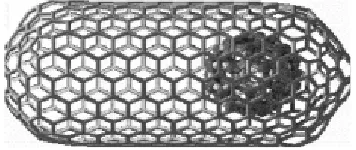
Graphite consists of sheets of carbon atoms in a hexagonal arrangement as shown in figure 4. The sheets are very loosely connected to each other. Now imagine taking a single sheet of graphite and cutting a long narrow strip. If that strip is rolled into a long, narrow tube, it would be a nanotube. The ends of the tubes usually form caps, as the dangling atoms will be receptive to forming bonds with their neighbors. The resulting structure is shown in Figure 5. The electrical property of the newly created nanotube depends upon the exact angle at which the graphite was cut.
Fig.5 A carbon nano tube
Fig.6 Bucky ball
A buckyball can be thought of as the smallest of the nanotubes. It is simply the connection of the two caps with no “tube” in between, and consists of exactly 60 carbon atoms (see Figure 6). Its combination of hexagons and pentagons is exactly the same as that found on a soccer ball. Very short nanotubes with 70, or even 80 atoms are sometimes also called buckyball.
3.1 The Nanomemory Device
The proposed nanomemory device (NMD) consists of two parts: the “capsule” which holds the much smaller, charged “shuttle”. The shuttle is a buckyball and it contains a potassium ion (K+) which gives the shuttle its
charge. (The potassium ion is not shown in the figure). The state of the memory device is determined by the location of the shuttle: if it is on one side of the capsule, we treat it as a ‘1’; on the other we treat it as a ‘0’. The Van der Waals forces between the tube and the shuttle will tightly bind the shuttle to one end of the tube or the other. There is an unstable equilibrium point when the shuttle is in the exact middle of the capsule, but application of certain voltage to the capsule would prevent the shuttle from ever coming to rest there.[7]
Fig. 7 An example nanomemory device
3.1.1 Writing to the NMD :
Writing to the device is easier than reading from it. To write, voltage is applied to the capsule and shuttle will move to the either side of the capsule. To move the shuttle to the other side same voltage with opposite polarity is applied. In general the amount of voltage which needs to be applied depends upon the length of the capsule. A field of 0.1 volts/c is sufficient to move the shuttle from one side of the tube to the other. Because of a bouncing effect buckyball takes time to come to a stop. Time to settle will be about 20 picoseconds.[7]
3.1.2 Reading from the NMD
Number of ways are proposed to perform a read.
The first requires three wires to be connected to the capsule: one on each end, and one in the middle. The position of the buckyball is detected by examining the resistance between the middle wire of the nanotube and the ends. A lower resistance will be found on the end that has the shuttle. This three-wire solution has a number of problems, not the least of which is that making a connection to the middle of a nanotube seems difficult. However, a long capsule and shuttle would perhaps make this solution viable.
a read that many shuttles can be used inside the capsule to increase the amount of the current flow.
[7]
3.2 Bi-layer CNT RAM
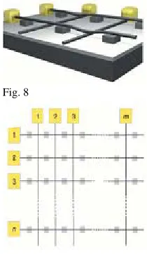
This device consists of a set of parallel SWNT(single wall nano tubes) or nanowires on a substrate and a set of perpendicular SWNTs that are suspended on a periodic array of supports (Figure 8 ). Each cross point in this structure corresponds to a device element with a SWNT suspended above a perpendicular nanoscale wire. Qualitatively, bistability can be envisioned as arising from the interplay of the elastic energy, which produces a potential energy minimum at finite separation (when the upper nanotube is freely suspended), and the attractive van der Waals (vdW) energy, which creates a second energy minimum when the suspended SWNT is deflected into contact with the lower nanotube. These two minima correspond to well defined OFF and ON states, respectively; that is, the separated upper-to-lower nanotube junction resistance will be very high, whereas the contact junction resistance will be orders of magnitude lower. A device element could be switched between these well-defined OFF and ON states by transiently charging the nanotubes to produce attractive or repulsive electrostatic forces. On the basis of this switching mode, we can characterize the elements as nano- or molecular-scale electromechanical devices. [1]
Fig. 8
Fig.9
Fig.10
Challenges with this device
The distance between the crossed wires has to be controlled fairly precisely: one to two nanometers Aligning a large number of these cross-wires and to make this pattern of nanotubes with precise control of distance is going to be a difficulty.
4. Conclusions
The potential and maturity of the emerging memory devices are reviewed in this paper to identify the most scientific and technological challenges that must be overcome by the device to become a viable technology.
References
[1] Thomas Rueckes, Kyoungha Kim, Ernesto Joselevich, Greg Y. Tseng, Chin Li Cheung, and Charles M. Lieber, ”Carbon Nanotube-Based Nonvolatile Random Access Memory for Molecular Computing”, Science Vol. 289, no. 5476 (July 7, 2000), pp. 94–97.
[2] The international technology Roadmap for semiconductor 2009.
[3] The international technology Roadmap for semiconductor 2011.
[4] Yiming Huai, “Spin-Transfer Torque MRAM (STT-
MRAM):Challenges and Prospects” AAPPS Bulletin December 2008, Vol. 18, No. 6
[5] Jim Hutchby & Mike Garner, "Assessment of the Potential & Maturity of Selected Emerging Research Memory Technologies ", in Workshop & ERD/ERM Working Group Meeting (April 6-7, 2010).
[6] Emre kultu rsay, Mahmut kandemir, Anand sivasubramaniam, onur Mutlu, “ Evluating STT-RAM as an Energy Efficient Main Memory Alternative”
[7] M Brehob, “The Potential of Carbon based Memory Systems”, IEEE 1999.
Authors
Minal Dubewar: She received B.E. degree in electronics and telecommunication from MGM College of Engineering affiliated to SRTM University in May-2007 and currently doing ME in Electronics from Shah & Anchor Kutchhi Engineering College affiliated to Mumbai University.
Nibha Desai: She received B.E. degree in electrical engineering from L D College of Engineering affiliated to Gujrat University in July-2004 and ME in Electronics from FRCRCE affiliated to Mumbai University in Dec 2012. Currently she is working as Assistant Professor in Shah and Anchor college of engineering, Mumbai.