Scholarship@Western
Scholarship@Western
Electronic Thesis and Dissertation Repository
2-7-2011 12:00 AM
Synthesis of One-Dimensional And Two-Dimensional Carbon
Synthesis of One-Dimensional And Two-Dimensional Carbon
Based Nanomaterials
Based Nanomaterials
Mihnea Ioan Ionescu
The University of Western Ontario Supervisor
Xueliang Sun
The University of Western Ontario
Graduate Program in Mechanical and Materials Engineering
A thesis submitted in partial fulfillment of the requirements for the degree in Doctor of Philosophy
© Mihnea Ioan Ionescu 2011
Follow this and additional works at: https://ir.lib.uwo.ca/etd
Part of the Materials Science and Engineering Commons, and the Nanoscience and Nanotechnology Commons
Recommended Citation Recommended Citation
Ionescu, Mihnea Ioan, "Synthesis of One-Dimensional And Two-Dimensional Carbon Based Nanomaterials" (2011). Electronic Thesis and Dissertation Repository. 83.
https://ir.lib.uwo.ca/etd/83
This Dissertation/Thesis is brought to you for free and open access by Scholarship@Western. It has been accepted for inclusion in Electronic Thesis and Dissertation Repository by an authorized administrator of
(Spine title: Synthesis of 1D and 2D Carbon based Nanomaterials)
(Thesis format: Integrated-Article)
by
Mihnea Ioan Ionescu
Graduate Program in Mechanical and Materials Engineering
A thesis submitted in partial fulfillment of the requirements for the degree of
Doctor of Philosophy
The School of Graduate and Postdoctoral Studies The University of Western Ontario
London, Ontario, Canada
ii
CERTIFICATE OF EXAMINATION
Supervisor
______________________________ Dr. Xueliang Sun
Supervisory Committee
______________________________ Dr. Jun Yang
Examiners
______________________________ Dr. Jeff Wood
______________________________ Dr. Jun Yang
______________________________ Dr. Paul Charpentier
______________________________ Dr. Gu Xu
The thesis by
Mihnea Ioan Ionescu
entitled:
Synthesis of One-Dimensional and Two-Dimensional Carbon Based Nanomaterials
is accepted in partial fulfillment of the requirements for the degree of
Doctor of Philosophy
______________________ _______________________________
iii
Particular physical and chemical properties of carbon based nanomaterials
(CBNs) have promised and exhibited great applications in manufacturing various
nanodevices such as electron field emitters, sensors, one-dimensional conductors,
supercapacitors, reinforcing fibres, hydrogen storage devices, and catalyst supports for
fuel cells electrodes. Despite these amazing technical progresses, many challenges still
remain in the development of synthesis methods suitable for commercial applications
and fabricating novel functional nanostructures with complex architectures.
In this Ph.D. thesis, one-dimensional (1D), two-dimensional (2D) carbon
nanostructures, and 1D/2D hybrid of carbon nanostructures have been synthesized using
various chemical vapour deposition (CVD) methods. The objective of this work is to
explore the potential of various CVD methods, including specially-designed CVD
techniques, such as modified spray pyrolysis, plasma enhanced CVD, and magnetron
sputtering deposition. By making use of these innovative methods, high density regular
and nitrogen-doped nanotubes, graphite nanosheets and assemblies have been
successfully obtained on conducting and semiconducting substrates. For the modified
spray pyrolysis method, systematic investigation of regular carbon nanotubes (CNTs)
was conducted in terms of optimizing various experimental parameters such as
hydrocarbon source, temperature, and catalyst in order to control the quality and
structure of CBNs. Doping of nitrogen into carbon nanotubes was also systematically
iv
spray pyrolysis method. By employing the plasma assisted CVD/sputtering hybrid
system, selective growth of single and few walled CNTs have been realized. The device
has also been able to produce 2D carbon nanostructures of nanosheets and a hybrid of
nanosheets suspended on vertical aligned CNTs. Based on the magnetron sputtering
deposition method, carbon nanowalls have been synthesized without any catalyst
addition. Morphology, microstructure, and vibration properties of the CBNs were
characterized by scanning electron microscopy, transmission electron microscopy,
Raman spectroscopy, and X-ray photoelectron spectroscopy.
Carbon nanomaterials, grown in high densities on conducting and
semiconducting substrates, promise great potential in building various nanodevices with
different electron conducting requirements. In addition, CBNs provide a very high
surface area for the support of platinum particles for use in hydrogen fuel cell
electrodes.
Keywords: Carbon, Nanomaterials, Carbon Based Nanomaterials, Nanotubes, Doped
Nanotubes, Branched Nanotubes, Graphite Sheets, Nanowalls, Chemical Vapor
v
Chapter 4: Mihnea Ionescu – designed and implemented the experimental device,
conducted the experiments, collected and analyzed the data, and wrote the chapter;
Yong Zhang – helped to acquire the Raman spectra, reviewed, and revised the chapter;
Ruying Li – helped to acquire the SEM images and acquired the TEM images; Xueliang
Sun – guided the experiments and revised the chapter; Hakima Abou-Rachid – made
revisions and recommendations to the chapter; Louis-Simon Lussier – revised the
chapter.
Chapter 5: Mihnea Ionescu – improved the design of the experimental device,
conducted the experiments, design and implemented the electrical characterization
setup, collected and analyzed the data, and wrote the chapter; Yong Zhang – helped to
analyze the XPS data and to acquire the Raman spectra, reviewed, and revised the
chapter; Ruying Li – helped to acquire the SEM images and acquired the TEM images;
Xueliang Sun – guided the experiments and revised the chapter.
Chapter 6: Mihnea Ionescu – innovated and implemented the design of the
experimental device, conducted the experiments, collected and analyzed the data, and
wrote the chapter; Yong Zhang – helped to acquire the Raman spectra, reviewed, and
revised the chapter; Ruying Li – helped to acquire the SEM images and acquired the
vi
Lussier – revised the chapter.
Chapter 7: Mihnea Ionescu – conducted the experiments, design and implemented the
electrical characterization setup, collected and analyzed the data, and wrote the chapter;
Yong Zhang – helped to acquire the Raman spectra, reviewed, and revised the chapter;
Ruying Li – helped to acquire the SEM images and acquired the TEM images; Xueliang
Sun – guided the experiments and revised the chapter.
Chapter 8: Mihnea Ionescu – innovated and implemented the design of the
experimental device, conducted the experiments, collected and analyzed the data, and
wrote the chapter; Yong Zhang – helped to acquire the Raman spectra, reviewed, and
revised the chapter; Ruying Li – helped to acquire the SEM images and acquired the
TEM images; Xueliang Sun – guided the experiments and revised the chapter.
Chapter 9: Mihnea Ionescu – innovated and implemented the design of the
experimental device, conducted the experiments, collected and analyzed the data, and
wrote the chapter; Yong Zhang – helped to acquire the Raman spectra, reviewed, and
revised the chapter; Ruying Li – helped to acquire the SEM images and acquired the
vii
viii
I genuinely thank my research advisor, Prof. Xueliang Andy Sun, for his
encouragement, support, patience, advice, and guidance during my whole study period.
I am grateful for offering me the opportunity to be part of his Nanomaterials and Energy
research group. I doubt that I will ever be able to convey my appreciation fully, but I
owe him my deepest gratitude.
I would like to express my special thanks to Mrs. Ruying Li (Kathy), for
providing me with understanding and support. Her advice, encouragement, and
kindness played an essential role in the development of this thesis by helping me
overcome many obstacles.
I wish to extend my sincere appreciation to Dr. Yong Zhang (Bryan), for taking
time out from his busy schedule to review and revise my scientific writing. His hard
work, advice, help and our fruitful discussions were crucial in finalizing and refining
this thesis.
Sincere thanks to Dr. Jun Yang for following my research progress and for
accepting to be part of the Supervisory Committee.
I would like to thank all my colleagues from Nanomaterials and Energy research
group. They have created a friendly, highly professional, and wonderful study
environment which has made the whole learning journey worthwhile.
I recognize that this research would not have been possible without the financial
ix
Ontario (Teaching Assistantships, Graduate Research Scholarships), and the Province
of Ontario Graduate Scholarship fund, and express my acknowledgement to these
agencies.
I will never have enough words of gratitude and love for my family and friends.
Your love, care, and unconditional support brought happiness into my life. Thank you
for showing me a great deal about who I am and who I’d like to become. Last, but
certainly not least, I need to thank my wife and best friend, Betty, who surrounded me
with love and encouragement. Without your help and editing assistance, I would never
have managed to finish this thesis. You’re a real trouper to have stuck with me through
x
CERTIFICATE OF EXAMINATION ...ii
ABSTRACT ... iii
CO-AUTHORSHIP ... v
DEDICATION ...vii
ACKNOWLEDGEMENTS ... viii
TABLE OF CONTENTS ... x
LIST OF TABELS ... xvi
LIST OF FIGURES ...xvii
LIST OF SYMBOLS ... xxiii
CHAPTER 1: GENERAL INTRODUCTION ... 1
1.1 Nanotechnology ... 1
1.2 Carbon nanomaterials ... 2
1.3 Thesis objectives and structure ... 4
1.4 References ... 6
CHAPTER 2: LITERATURE REVIEW ... 8
2.1 Carbon materials ... 8
2.1.1 Electronic structure of a single carbon atom ... 9
2.1.2 Hybridization of carbon atoms ... 10
2.1.2.1 sp hybridization ... 11
2.1.2.2 sp2 hybridization ... 12
2.1.2.3 sp3 hybridization ... 13
xi
2.1.3.2 Graphite ... 16
2.1.3.3 Diamond ... 18
2.1.4 Other forms of carbon ... 20
2.1.4.1 Amorphous carbon ... 20
2.1.4.2 Glass-like carbon ... 21
2.1.4.3 Carbon blacks ... 23
2.1.5 Phase diagram of carbon ... 24
2.1.6 Carbon based nanomaterials ... 26
2.1.6.1 Fullerenes ... 27
2.1.6.1.1 Spherical fullerenes ... 27
2.1.6.1.2 Carbon nanotubes ... 29
2.1.6.2 Carbon nanofibers ... 33
2.1.6.3 Graphenes ... 34
2.1.6.4 Carbon nanowalls ... 36
2.2 Synthesis methods review on carbon based nanomaterials ... 37
2.2.1 Synthesis of zero-dimensional spherical fullerenes ... 37
2.2.2 Synthesis of one-dimensional carbon nanotubes ... 39
2.2.2.1 Synthesis of regular CNTs ... 39
2.2.2.1.1 Arc discharge method ... 40
2.2.2.1.2 Laser ablation method ... 41
2.2.2.1.3 Thermal chemical vapor deposition method ... 42
2.2.2.1.4 Floating catalyst chemical vapor deposition method ... 44
2.2.2.1.5 Aerosol assisted chemical vapor deposition method ... 45
xii
2.2.2.1.8 Other methods used for CNT production ... 48
2.2.2.1.9 Growth mechanism of CNTs ... 49
2.2.2.2 Doped CNTs ... 52
2.2.2.2.1 General review on doped CNTs ... 52
2.2.2.2.2 Nitrogen doped CNTs ... 53
2.2.2.2.3 Growth mechanism of nitrogen doped CNTs ... 55
2.2.3 Synthesis of two-dimensional graphenes ... 57
2.3 The future of carbon based nanomaterials ... 58
2.4 References ... 60
CHAPTER 3: EXPERIMENTAL PROCEDURES ... 74
3.1 Synthesis processes ... 74
3.1.1 Catalyst preparation ... 74
3.1.2 The growth based on plasma enhanced CVD system ... 75
3.1.3 The growth based on spray pyrolysis CVD system ... 77
3.2 Microstructure characterization ... 79
3.3 Property evaluation ... 79
3.3.1 Evaluation techniques ... 79
3.3.2 Microprobes sensing elements fabrication ... 80
3.3.2 Field emission measurements ... 81
3.4 References ... 82
CHAPTER 4: SPRAY PYROLYSIS CHEMICAL VAPOR DEPOSITION METHOD FOR THE CARBON NANOTUBE GROWTH PARAMETRIC STUDIES ... 84
4.1 Abstract ... 84
xiii
4.4 Results and discussion ... 88
4.4.1 Effect of temperature ... 88
4.4.2 Effect of precursor flow rate ... 91
4.4.3 Effect of catalyst concentration ... 93
4.4.4 Effect of injected volume ... 97
4.4.5 Effect of substrate ... 98
4.5 Conclusions ... 101
4.6 References ... 102
CHAPTER 5: NITROGEN-DOPING EFFECTS ON THE GROWTH, STRUCTURE, AND ELECTRICAL PERFORMANCE OBTAINED BY SPRAY PYROLYSIS METHOD ... 106
5.1 Abstract ... 106
5.2 Introduction ... 107
5.3 Experimental ... 108
5.4 Results and discussion ... 110
5.4.1 Structure and composition of CNx ... 111
5.4.2 Electrical resistivity of bulk CNx ... 118
5.5 Conclusions ... 121
5.6 References ... 121
CHAPTER 6: CONTROLLED SYNTHESIS OF A NOVEL CLASS OF CARBON NANOSTRUCTURES: MULTIPLE-LEVEL HIERARCHICAL N-DOPED CARBON NANOTUBES ... 126
6.1 Abstract ... 126
6.2 Introduction ... 127
xiv
6.4.1 Effect of precursors ... 133
6.4.2 Effect of growth time ... 134
6.4.3 Effect of precursor flow rate ... 137
6.4.4 Effect of catalyst concentration ... 139
6.4.5 Effect of temperature ... 140
6.4.6 Effect of substrates ... 142
6.4.7 Growth Mechanism ... 143
6.5 Conclusions ... 145
6.6 References ... 146
CHAPTER 7: SELECTIVE GROWTH, CHARACTERIZATION, AND FIELD EMISSION PERFORMANCE OF SINGLE-WALLED AND FEW-WALLED CARBON NANOTUBES BY PLASMA ENHANCED CHEMICAL VAPOR DEPOSITION ... 148
7.1 Abstract ... 148
7.2 Introduction ... 149
7.3 Experimental ... 151
7.4 Results and discussion ... 154
7.4.1 Influence of substrate temperature ... 154
7.4.2 Influence of plasma power and substrate to plasma distance ... 156
7.4.3 Influence of catalyst thickness ... 158
7.4.4 Structure characterization of FWCNTs and SWCNTs ... 160
7.4.5 Field emission performance of FWCNTs and SWCNTs ... 164
7.5 Conclusions ... 166
xv
DEPOSITION ... 171
8.1 Abstract ... 171
8.2 Introduction ... 172
8.3 Experimental ... 173
8.4 Results and discussion ... 174
8.5 Conclusions ... 183
8.6 References ... 183
CHAPTER 9: SYNTHESIS OF FREESTANDING CARBON NANOWALLS BY MAGNETRON SPUTTERING ... 187
9.1 Abstract ... 187
9.2 Introduction ... 187
9.3 Experimental ... 188
9.4 Results and discussion ... 190
9.5 Conclusions ... 195
9.6 References ... 195
CHAPTER 10: CONCLUSIONS, FUTURE WORK, AND RECOMENDATIONS .... 198
10.1 Conclusions ... 198
10.2 Future work ... 200
10.3 Recommendations ... 201
xvi
Table 5.1 Dependence of nitrogen doping, structure and size of the CNx on ratios of
xvii
Figure 2.1 Diagram of the electronic structure of the carbon atom in the ground state (a)
and the energy level chart (b). ... 10
Figure 2.2 sp hybridization of carbon. ... 12
Figure 2.3 sp2 hybridization of carbon. ... 13
Figure 2.4 sp3 hybridization of carbon. ... 14
Figure 2.5 The hexagonal form of graphite. ... 17
Figure 2.6 The cubic form of diamond. ... 19
Figure 2.7 View of a-C network showing deviations in both bonding distances and angles for the sp2 and sp3 hybridized atoms. ... 20
Figure 2.8 Schematic diagram for the microstructure of the closed pore structure model for glassy carbon. ... 22
Figure 2.9 Schematic view of a carbon black particle showing short graphitic segments.23 Figure 2.10 Phase diagram of carbon after F.P. Bundy. ... 25
Figure 2.11 View of stable fullerenes C60 (a) and C76 (b). ... 28
Figure 2.12 Graphite layer with atoms labeled using (n, m) notation and different types of CNTs. ... 31
Figure 2.13 The structure of “stacked” (a) and “herringbone” (b) nanofibers (the arrow indicates the fiber axis). ... 34
Figure 2.14 Graphene as a 2D building material for carbon materials of all other dimensionalities: 0D fullerenes, 1D nanotubes or 3D graphite. ... 35
Figure 2.15 Schematic diagram of fullerene synthesis device - combustion method. ... 38
xviii
Figure 2.18 Schematic diagram of a thermal CVD setup. ... 43
Figure 2.19 Schematic diagram of a FCCVD setup. ... 44
Figure 2.20 Schematic diagram of an AACVD setup. ... 45
Figure 2.21 Schematic diagram of spray pyrolysis CVD setup. ... 47
Figure 2.22 Schematic diagram of PECVD deposition system. ... 48
Figure 2.23 Diagram of the growth model of CNTs for arc discharge and laser ablation methods. ... 50
Figure 2.24 Diagram of the CNTs tip growth model (a) and base growth model (b). ... 51
Figure 2.25 Bonding configurations for nitrogen atoms in CNTs; graphitic nitrogen (a), pyrrolic-type nitrogen (b), pyridine-like nitrogen (c). ... 55
Figure 2.26 Diagram of the formation of a bamboo cavity in CNx. ... 56
Figure 3.1 Image and schematic diagram of PECVD/sputtering hybrid deposition system. ... 76
Figure 3.2 Image of spray pyrolysis deposition system (a), view of the pulverized droplets (b), and schematic diagram of deposition system (c). ... 78
Figure 3.3 Schematic diagram of the two-points microprobe fabrication. ... 80
Figure 3.4 Schematic diagram of the planar diode configuration. ... 81
Figure 4.1 Schematic diagram of spray pyrolysis CVD system. ... 87
xix
µ
precursor flow rate (b); average nanotube diameter function of flow rate (c). ... 92
Figure 4.4 SEM images of cross-sectional view of VA-CNT arrays obtained using 0.1%
ferrocene in xylene, 0.5%, 1%, 2.5%, and 5% (a); diagrammatic relationship between
the average nanotube length and ferrocene concentration (b); diagrammatic relationship
between the average nanotube diameter and ferrocene in xylene concentration, and the
occurrence of bimodal diameter distribution (c). ... 94
Figure 4.5 SEM image for nanotubes synthesized at 5 % ferrocene in xylene
concentration (a); TEM image for nanotubes synthesized at 5 % ferrocene in xylene
concentration (b); SEM image for nanotubes synthesized at 0.5 % ferrocene in xylene
concentration (c); TEM image for nanotubes synthesized at 0.5 % ferrocene in xylene
concentration (d); diameter distribution of nanotubes obtained at 0.5 % and 5 %
ferrocene in xylene concentrations (e); Raman spectra of nanotubes synthesized at 0.5
% and 5 % ferrocene in xylene concentrations (f). ... 96
Figure 4.6 SEM image of the nanotubes synthesized using 0.3 ml active solution (a); 30
ml active solution (b); diagrammatic relationship between the average nanotube length
and volume of the injected solution (c); SEM image of the nanotube roots (d). ... 98
Figure 4.7 SEM image of CNTs grown on CP (a, b); SEM image of CNTs grown on SS
(c, d); TEM image of CNTs grown on SS (e); Raman spectra of nanotubes synthesized
on CP and SS (f). ... 100
Figure 5.1 Schematic diagram of spray pyrolysis CVD system for CNx synthesis. ... 109
Figure 5.2 Electron microscopic images showing average CNT length (a) (inset:
diagram of the relationship between acetonitrile:xylene concentration and average CNT
length) and nanotubes at the bottom (b,c) and tip part (d). ... 112
Figure 5.3 TEM images of the CNT structure, schematic diameter distribution, and
Raman spectrum for samples produced using pure xylene (a-d), 50 vol% concentration
xx
Figure 5.5 I–V characteristics of regular nanotubes for temperatures between 35 oC and
125 oC (a). A plot of resistivity vs. temperature for bulk CNTs with different nitrogen
content (b). ... 119
Figure 5.6 A plot of electrical resistance vs. pressure for bulk CNTs with different
nitrogen content. ... 120
Figure 6.1 Schematic diagram of the spray pyrolysis CVD apparatus with the injection
device. ... 129
Figure 6.2 SEM image of a well-aligned branched CNTs array (a); view of catalyst
particles at the bottom ends of CNTs (b); nanotube branch occurence at the same height
(c); view of the top part of branched CNTs (d). ... 130
Figure 6.3 TEM images of the branched CNTs (a); view of the stalk nanotube with a
catalyst inclusion (b); view of the nanotube branch occurrence (c); view of the
first-level nanotubes (d). ... 132
Figure 6.4 SEM images of the CNTs using different precursors: xylene (a), ethanol (b),
melamine in ethanol (c), and melamine in pyridine (d). ... 134
Figure 6.5 SEM images of the CNTs obtained after a growth time of 10 min (a), 20 min
(b), 30 min (c), 40 min (d), and 60 min (e). ... 136
Figure 6.6 SEM images of the branched nanotubes obtained at different precursor flow
rates: 0.02 ml/min (a), 0.06 ml/min (b), and 0.1 ml/min (c). TEM image of the branched
nanotubes showing the amount of branches derived from a single stalk nanotube
obtained at a flow rate of 0.06 ml/min (d). ... 138
Figure 6.7 SEM images of the CNTs using different concentrations of ferrocene: 2.5
wt% (a) and (b), 0.5 wt% (c) and (d). ... 140
Figure 6.8 SEM (a) and TEM (b) images of the CNTs deposited at 800 oC; SEM (c) and
xxi
Figure 6.10 Schematic diagram of the growth mechanism of the multi-level N-doped
carbon nanotubes. ... 144
Figure 7.1 Schematic diagram of PECVD deposition system – RF plasma source (A);
matching box, and generators (B); substrate heating element with vertical movement
(C); mass flow controller for gas inlets (D); connection to vacuum pump (E);
connection to vacuum gauge (F); magnetron (G). ... 152
Figure 7.2 SEM images of the CNTs obtained at 450 °C (low magnification) (a); 450 °C
(high magnification) (b); 550 °C (low magnification) (c); 550 °C (high magnification)
(d); 700 °C (low magnification) (e); 700 °C (high magnification) (f); illustration of the
average tube length with temperature (g). ... 155
Figure 7.3 SEM images of the CNTs obtained at 50 W plasma power (a) and 300 W (b);
plasma to substrate distance of minimum 8 cm (c), and 16 cm (d). Plots of average
nanotube length vs. plasma power (e) and substrate to plasma distance (f). ... 157
Figure 7.4 SEM images of the carbon nanotubes grown with the thickness of 7 nm Fe
(low magnification) (a); 7 nm Fe (high magnification) (b); 3 nm Fe (low magnification)
(c); 3 nm Fe (high magnification) (d); 1 nm Fe (e); A plot of CNT average thickness vs.
catalyst thickness (f). ... 159
Figure 7.5 Characterization of the samples obtained for 3 nm catalyst thickness – Low
magnification TEM image of the FWCNT bundles (a); Magnified TEM image of the
FWCNTs (b); Raman spectrum of the FWCNTs (c). ... 161
Figure 7.6 Characterization of the samples obtained for 1 nm catalyst thickness – TEM
image of the nanotube bundles (a); Raman spectrum (b); RBM region (c); RBM from a
single bundle of the CNTs (d). ... 163
Figure 7.7 Curves of current density vs. electric field and Fowler-Nordheim plots for
the SWCNTs (curve (1)) and for FWCNTs (curve (2)). ... 164
xxii
view from CNTs side (d); hybrid carbon nanostructure detached from the substrate (e)
view of aligned CNTs at high magnification (f). ... 175
Figure 8.3 TEM image of hybrid carbon nanostructure showing the inclusion of
numerous granular domains in the carbon nanosheet (a); TEM image indicating CNTs
connected with nanoparticles (b); SEM image indicating CNTs connected with
nanoparticles (c). ... 176
Figure 8.4 SEM images of hybrid carbon nanostructure showing the CNTs height for
different deposition time: 5 min – 300 nm (a); 10 min – 600 nm (b); 20 min – 1.1 µm
(c). ... 177
Figure 8.5 SEM images of carbon nanosheet obtained without Al2O3 underlayer. ... 179
Figure 8.6 SEM images of carbon nanostructure hybrid obtained in two steps. ... 180
Figure 8.7 Raman spectra of carbon nanosheets (curve a); carbon nanosheet sustained
on CNTs (curve b); carbon nanostructure hybrid obtained in two steps (curve c). ... 181
Figure 9.1 Schematic diagram of the PECVD/sputtering hybrid system deposition
system. ... 189
Figure 9.2 SEM images of carbon nanowalls at different magnifications. ... 190
Figure 9.3 TEM images of carbon nanosheets show large area (a) of continuous and
corrugated structure (b); Raman spectrum of the carbon nanowalls (c). ... 191
Figure 9.4 SEM images of CNWs grown under a hydrogen flow of 50 sccm (a); CNWs
xxiii
0D Zero Dimensional
1D One Dimensional
2D Two Dimensional
AACVD Aerosol Assisted Chemical Vapor Deposition
C60 Buckminsterfullerene
CBN Carbon Based Nanomaterial
CNS Carbon Nanosheet
CNT Carbon Nanotubes
CNW Carbon Nanowall
CNx Nitrogen-Doped Carbon Nanotube
CVD Chemical Vapor Deposition
DC Direct Current
DLC Diamond-Like Carbon
EELS Electron-Energy Loss Spectroscopy
FCCVD Floating Catalyst Chemical Vapor Deposition
FLG Few-Layer Graphene
FWCNT Few-Walled Carbon Nanotube
GLC Glass-Like Carbon
HiPCO High Pressure Carbon Monoxide
xxiv ITO Indium Tin Oxide
MWCNT Multi-Walled Carbon Nanotube
PECVD Plasma Enhanced Chemical Vapor Deposition
RBM Radial Breathing Mode
RF Radio Frequency
SEM Scanning Electron Microscopy
SS Stainless Steel
SWCNT Single-Walled Carbon Nanotube
TCR Temperature Coefficient of Resistance
TEM Transmission Electron Microscopy
VA-CNT Vertically Aligned Carbon Nanotube
CHAPTER 1
GENERAL INTRODUCTION
1.1 Nanotechnology
Nanotechnology is the study and creation process of functional and useful
materials, devices, and systems through control of matter at the nanometer scale,
generally between 1 to 100 nanometers in at least one dimension. The study of physical
properties of nanoscale materials have led to numerous new applications. The aim of
nanotechnology is to make use of these properties and efficiently manufacture and
generate larger structures with fundamentally new molecular organization [1].
Theoretically, this possibility was envisioned in 1959 by Richard Feynman [2]. The term
‘nanotechnology’ was popularized by K. Eric Drexler, when he exposed ideas about
building machines at the molecular scale, far smaller than a cell. Drexler spent years
analyzing these incredible devices and finally published a milestone book in the 1990’s:
“Nanosystems: Molecular Machinery, Manufacturing, and Computation” [3, 4]. At that
time, fullerenes and nanotubes were just discovered and nanotechnology became an
accepted concept [5, 6]. Nanoscale materials such as nanotubes, nanowires, and nanobelts
have extraordinary properties and unique geometric features [7]. These are exciting
discoveries of the last two decades which have given a great impulse to the research on
nanomaterials. They have offered new opportunities of exploring distinct properties of
nanoscale and bringing these properties to the macroscale are difficult tasks. For this
reason, a new conceptual framework for nanotechnology development which takes into
consideration the present scientific potential [8] has been envisioned. It proposes an
interdisciplinary approach spanning across applied physics, materials science,
engineering, mechanics, electronics, and biology. The framework describes four
generations of nanotechnology development. The first generation of nanotechnology
products incorporates passive nanostructures and designed materials to perform one task.
The second phase introduces active nanostructures for multitasking such as actuators,
drug delivery devices, and sensors. The third generation features nanosystems with
thousands of interacting components built from the bottom-up, rather than manufactured
using top-down fabrication methods. Such achievements would lead to the fourth
generation which is expected to combine heterogeneous molecular systems. From this
point of view, the contemporary research performed in this area is not nanotechnology in
the original meaning of the word. Realistically, the nanotechnology development could
be considered at the end of the first generation [9]. From this perspective, the synthesis of
nanomaterials with controlled structure plays a crucial role in nanotechnology research
towards the second generation of nanotechnology development.
1.2 Carbon nanomaterials
Nanomaterials cover various types of nanostructured materials which posses at
have similar properties to their bulk counterparts, the properties of materials with
nanometer dimensions are significantly different from those of atoms and bulk materials
[7]. Carbon is a unique element due to its ability to form a variety of nanomaterials
ranging from zero-dimensional (0D) fullerenes to one-dimensional (1D) conducting and
semiconducting carbon nanotubes, and to two-dimensional (2D) semimetallic graphenes
[11]. These carbon based nanomaterials have remarkable physical properties and have
received specific attention for a variety of applications. It clearly appears that carbon
based materials constitute a topic of huge scientific interest and great strategic
importance, in which an interdisciplinary approach is necessary [12]. Although the study
of nanostructured carbon materials has recently undergone a steadily rapid development
and keeps a fast moving research field, the investigation still lacks in terms of
fundamental understandings of the growth mechanisms and key factors responsible for
the synthesis of carbon nanomaterials. Moreover, because the carbon phase diagram is far
from in-depth exploration, new forms of carbon are expected to be discovered. Carbon
based nanomaterials are currently considered a milestone in nanotechnology because they
provide an accelerated scientific progress with many industrial applications. Achieving
an enhanced degree of controllability and tuning capacity of material properties, would
lead to the accomplishment of the ultimate nanotechnological goal: the capability to
design and manufacture various complex three-dimensional hierarchical assembly
1.3 Thesis objectives and structure
Numerous studies of CNBs have previously been conducted in examining the
synthesis of 1D carbon nanotubes, their physical properties, and the influence of different
growth parameters. However, there have been few studies investigating the factors that
influence the nanotube growth in spray pyrolysis and plasma assisted deposition methods.
Less has been done with regards to the synthesis of 2D carbon nanostructures.
Consequently, this study is focused on the implementation of controllable synthesis
procedures and on the correlation between the applied growth parameters and the
structure of the obtained carbon based nanomaterials. 1D and 2D carbon based
nanostructures have been synthesized by employing different methods, such as spray
pyrolysis, plasma enhanced chemical vapor deposition (PECVD), and magnetron
sputtering.
The thesis consists in ten chapters organized in the following arrangement:
Chapter 1 generally introduces the background of nanotechnology and nanomaterials.
The research objectives and the thesis structure are outlined.
Chapter 2 is a review of the fundamental aspects of carbon materials with respect to the
structure and properties of different types of carbon materials. It also describes the most
important techniques presently used for carbon nanomaterials synthesis. In addition,
general considerations on doping carbon nanotubes are presented along with the growth
Chapter 3 outlines the experimental setups and provides information about the employed
characterization methods and procedures.
Chapter 4 proposes a modified spray pyrolysis chemical vapor deposition (CVD)
method for growing carbon nanotubes (CNTs) on electrically semiconducting and
conducting substrates without hydrogen addition. The experiments have been conducted
by optimizing the various parameters such as temperature, precursor flow rate, precursor
volume, and catalyst concentration.
Chapter 5 considers the study of nitrogen-doping effects on the growth and structure of
carbon nanotubes obtained by spray pyrolysis method. The nitrogen amount incorporated
in CNTs decreases the growth rate and influences the tubes structure, from straight to
corrugated nanotubes.
Chapter 6 outlines the synthesis of a new structure of nitrogen-doped and hierarchical
CNTs by spray pyrolysis CVD. The structure is highly controlled and consists of aligned
CNTs which have multiple-level branched structure with increasing mean diameters.
Chapter 7 focuses on the parameters effects on the growth of carbon nanotubes using
PECVD method. The parametric study includes the variation of the inductive power,
temperature, catalyst thickness, and plasma to substrate distance.
Chapter 8 proposes the synthesis of a hybrid of 1D/2D carbon nanostructures in a single
step by PECVD method. The hybrid is composed of two-dimensional carbon nanosheets
suspended on vertically aligned carbon nanotubes. The carbon nanosheets are detached
from the substrate by the first generation of vertical align CNTs and are covered by
Chapter 9 explores a new method of growing two-dimensional carbon nanowalls. In this
study, the magnetron sputtering technique is proposed for growing carbon nanowalls, on
semiconducting substrates, without catalyst addition.
Chapter 10 concludes and summarizes the findings from these studies. It also presents
experimental considerations for further improvements in future work.
1.4 References
[1] L.E. Foster, Nanotechnology: Science, Innovation, and Opportunity, Prentice Hall,
2009.
[2] R. Feynman, “There's plenty of room at the bottom,” Journal of
Microelectromechanical Systems, vol. 1, 1992, pp. 60-66.
[3] E. Drexler, Engines of Creation: The Coming Era of Nanotechnology, Anchor, 1987.
[4] K.E. Drexler, Nanosystems: Molecular Machinery, Manufacturing, and
Computation, Wiley, 1992.
[5] H.W. Kroto, J.R. Heath, S.C. O'Brien, R.F. Curl, and R.E. Smalley, “C60:
Buckminsterfullerene,” Nature, vol. 318, Nov. 1985, pp. 162-163.
[6] S. Iijima, “Helical microtubules of graphitic carbon,” Nature, vol. 354, Nov. 1991,
pp. 56-58.
[7] G. Cao, Nanostructures and Nanomaterials: Synthesis, Properties & Applications,
Imperial College Press, 2004.
[8] D.M. Bowman and G.A. Hodge, “Nanotechnology: Mapping the wild regulatory
frontier,” Futures, vol. 38, Nov. 2006, pp. 1060-1073.
[9] M.A. Ratner and D. Ratner, Nanotechnology: a gentle introduction to the next big
idea, Prentice Hall PTR, 2003.
[10] D. Vollath, Nanomaterials: An Introduction to Synthesis, Properties and
[11] T.C. Dinadayalane and J. Leszczynski, “Remarkable diversity of carbon–carbon
bonds: structures and properties of fullerenes, carbon nanotubes, and graphene,”
Structural Chemistry, 2010.
[12] A.L. Porter and J. Youtie, “How interdisciplinary is nanotechnology?,” Journal of
CHAPTER 2
LITERATURE REVIEW
2.1 Carbon materials
Carbon is a fascinating chemical element with unique properties. It is one of the
few elements known and used since antiquity. The name comes from Latin language
word “carbo” which means coal. No other element in the periodic table occurs in so many
different forms [1]. Coal, soot, graphite, and diamond are all nearly pure forms of carbon.
While graphite is soft enough to be used in pencils, diamond ranks among the hardest
materials known. Carbon has been used from ancient times, in charcoal form for bronze
production or as candle soot mixed with olive oil for writing. Some of the earliest cave
paintings, at Lascaux or Altamira, were realized using a mixture of charcoal and soot [2,
3]. Carbon based nanomaterials refer to solid carbon materials with structural units on a
nanometer scale in at least one direction. These materials have a large surface to volume
ratio reflected in their unique and remarkable properties. Carbon is accepted to be as
important for nanotechnology as silicon is for electronics [4]. The morphology of carbon
nanomaterials ranges from fullerenes to carbon nanotubes, from graphene to nanocones
or nanodiamonds. Carbon, the common element of these materials, continues to arouse
the interest and attention of researchers all over the world. This chapter is a review of the
most important aspects of the carbon materials, carbon nanomaterials, and their synthesis
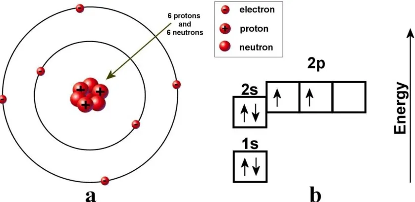
2.1.1 Electronic structure of a single carbon atom
Carbon is the chemical element with symbol C, atomic number 6. It is found in
the periodic table as a member of group 14. A carbon atom has six electrons with a
1s22s22p2 electronic ground state configuration. The two electrons contained in the 1s
orbital are strongly bound electrons and are called core electrons. The other four electrons
which occupy the 2s22p2 orbitals, are weakly bound electrons, and are called valence
electrons (Figure 2.1a). The actual location of electrons in a carbon atom cannot be
determined with certainty and the diagram can be misleading. A better way to look at the
carbon atom is by using an energy level chart shown in Figure 2.1b. The electrons are
represented by arrows while the direction of the arrow represents the spin of the electron.
Two electrons are found in the 1s orbital close to the nucleus. These two electrons, which
spin in opposite directions, have the lowest possible energy. They fill the K shell or first
shell as principal quantum number; K (n=1). Being filled, the K shell is completely stable
and its two electrons do not take part in any bonding. The four electrons belong to the L
shell; L (n=2). The L-shell has two different sub-shells, s and p. Two electrons fill the 2s
orbital and have opposite spin. The last two electrons partially fill the 2p orbital and have
parallel spin. The 2s and the 2p electrons have different energy levels. The 2p electrons
located in the outer orbital are the only electrons available for bonding to other atoms.
Figure 2.1 Diagram of the electronic structure of the carbon atom in the ground state (a)
and the energy level chart (b).
In this state carbon is divalent because only two electrons are available for bonding.
Divalent carbon is found in carbene, a class of highly reactive molecules. In contrast,
carbon allotropes and polymorphs are tetravalent and four valence electrons are present
for bonding the carbon atoms [5]. The description of how carbon electron valence is
increased to form carbon allotropes is outlined below.
2.1.2 Hybridization of carbon atoms
The electron configuration of the carbon atom has to be modified in order to allow
carbon atoms to combine themselves. The configuration of the carbon atom must be
mixing the orbitals of the outer shell of the atom in the ground state and, consequently,
forming new hybrid atomic orbitals. The concept is called hybridization. For carbon, one
2s electron is promoted into the 2p orbital. The remaining 2s orbital is spherically
symmetrical while the formed three 2p orbitals are oriented along the three axes
perpendicular to each other. The way of combining these different orbitals gives different
carbon hybridization types.
2.1.2.1 sp hybridization
In sp hybridization one s and one p (2px) orbital from the outer shell are altered to
form two equivalent orbitals called 'sp' hybrid orbitals directed towards the 'x' axis. This
hybridization is often known as diagonal hybridization as the two sp orbitals are at 180o
due to mutual repulsion of their electron clouds. The remaining 2py and 2pz orbitals do
not take part in hybridization and are directed along the 'y' and 'z' axes, perpendicular to
the two sp orbitals (Figure 2.2). The linear orientation of the sp orbitals is available to
form high strength sigma (σ) bonds while the non-hybridized p orbitals are available to
Figure 2.2 sp hybridization of carbon.
2.1.2.2 sp2 hybridization
In this type of hybridization, one s and two p orbitals (2px and 2py) get hybridized
to form three equivalent orbitals called 'sp2' hybrid orbitals. These identical orbitals are in
the same plane and their orientation is at 120o angle (Figure 2.3). Graphite is the typical
structure for sp2 hybridization of carbon. The planar orientation of the sp2 orbitals is
The un-hybridized orbital 2pz of carbon is oriented in a plane perpendicular to the plane
containing the three hybridized orbitals and is available to form π bonds.
Figure 2.3 sp2 hybridization of carbon.
2.1.2.3 sp3 hybridization
In the sp3 hybridization, the carbon atom has four sp3 orbitals of equivalent
repulsion of the electron clouds, are directed towards the four corners of a regular
tetrahedron with the carbon atom in the center. The angle between the hybrid orbitals is
approximately 109.5o. This structure is the basis of the diamond crystal. The four sp3
valence electrons of the hybrid carbon atom, in combination with the small size of the
atom, cause strong covalent σ bonds. Each tetrahedron of the hybridized carbon atom
(shown in Figure 2.4) combines with other four hybridized carbon atoms to form a
three-dimensional lattice structure.
2.1.3 Carbon allotropes
Allotropes are defined as the structural modifications of an element. Allotropism
is the property of chemical elements to exist in two or more different forms. The concept
of allotropy was originally proposed by the Swedish scientist Baron Berzelius in 1841
who reviewed the monoclinic and rhombic forms of sulfur [6]. Carbon has three main
allotropes: diamond, graphite, and carbyne. These forms represent the three types of
carbon hybridization: sp, sp2, and sp3. Fullerenes are a recently discovered form of pure
carbon and take the form of a hollow sphere, ellipsoid, or tube. Fullerene hybridization
falls between graphite (sp2) and diamond (sp3) due to the curvature of the surface [7] and
will be reviewed in a later paragraph.
2.1.3.1 Carbyne
Elemental carbon exists in three bonding states according to its hybridization.
Each type of hybridization should correspond to a certain form of carbon. Only two
forms of carbon related to the sp2 and sp3 hybridization were known up to 1960: graphite
and diamond. Therefore, it was reasonable to assume the existence of a material with
one-dimensional structure formed by carbon atoms sp hybridized [8]. For a long time
finding this carbon allotrope was the subject of great interest of both theoretical and
experimental research. At the end of the 19th century, several approaches were reported in
coupling reaction of ethynyl compounds as starting monomer. These experiments were
systematically investigated in 1959-1960 and culminated with the discovery of the linear
allotropic form of carbon [9]. This form was labeled carbyne from the Latin word
“carboneum” (carbon) and the suffix “yne” used in organic chemistry to designate an
acetylenic bond. Carbyne occurs in two forms: polyyne and cumulene. Polyyne is a linear
chain-like form of alternating single and triple bonds (–C≡C–)n, while cumulene contains
double bonds of carbon atoms (=C=C=)n [10]. Carbyne was found as a natural mineral in
1968 in the Ries meteorite crater (Germany) and was named “chaoite” in the honor of the
respected scientist E. Chao. Carbynes have drawn considerable interest in
nanotechnology as its Young's modulus is forty times that of diamond [11]. To date, the
longest polyyne synthesized is a chain of 44 carbon atoms [12].
2.1.3.2 Graphite
Graphite, the sp2 hybridized form of carbon, was named in 1789 from the Greek
word “graphein” (to draw, to write). Graphite has a layered hexagonal planar structure.
The hexagonal layers are held parallel with each other by Van der Waals forces. In each
layer, the hexagonal lattice is formed by carbon atoms with separation of 0.142 nm, and
the distance between planes is 0.335 nm [13]. The chemical bonds within the layers are
covalent with sp2 hybridization. Two forms of graphite are known, hexagonal and
rhombohedral. Although these have graphene layers which stack differently, they have
graphite with an ABAB stacking sequence of the graphene layers (Figure 2.5). The unit
cell dimensions are a=0.2456 nm and c=0.6708 nm [14]. Hexagonal graphite is
thermodynamically stable below approximately 2600 K and 6 GPa [15]. The
rhombohedral graphite is thermodynamically unstable with an ABCABC stacking
sequence of the layers. The unit cell constants are a=0.2566 nm and c=1.0062 nm [16].
This form has not been isolated in pure form. It is always mixed with the hexagonal form
in variable amounts which can be increased up to 40% of rhombohedral content. Heating
to above 1600 K progressively transforms rhombohedral graphite to hexagonal graphite,
which shows that the hexagonal phase is thermodynamically more stable [17].
2.1.3.3 Diamond
Diamond is an allotrope of carbon. Diamonds were discovered in India about
6000 years ago in the riverbeds of the region. The name diamond is derived from the
ancient Greek "adamas" meaning unbreakable, untamed and unconquerable. In 1772, it
was proved that diamond is composed of carbon [18]. It is the hardest naturally occurring
mineral and ranks among the rarest materials known. Most natural diamonds are formed
at high-pressure and high-temperature conditions in the Earth mantle and are brought
close to the surface through volcanic eruptions. Diamonds can also be produced
synthetically by processes which simulates the conditions in the Earth mantle or by
chemical vapor deposition [19]. Despite its hardness, the chemical bonds that hold
together the carbon atoms are weaker in diamond than in graphite. The difference is that
in diamond the covalent bonding between the carbon atoms has sp3 hybridization and
forms an inflexible and strong three-dimensional lattice. In graphite, the atoms are
strongly bonded in sheets, but the sheets are weakly bonded and slide easily [20]. Two
forms of diamond are known with cubic and hexagonal crystal structure. Frequently,
diamond is found in the cubic form which is thermodynamically stable at pressures above
6 GPa at room temperature and metastable at atmospheric pressure. At low pressures
cubic diamond converts rapidly to graphite at temperature above 1900 K in an inert
atmosphere [21]. Under ambient conditions such transformation is negligibly slow. In the
cubic form, each carbon atom is linked to four other carbon atoms in a tetrahedral array
(Figure 2.6). The bond length between two carbon atoms is 0.154 nm [22]. Pure diamond
is called lonsdaleite or hexagonal diamond. It is thought to occur when meteoric graphite
falls to Earth. The heat and stress from the impact transform the graphite into a structure
similar to diamond. The properties of this material are not well known due to the limited
existent amount of lonsdaleite. Using computer simulation techniques, it was shown that
lonsdaleite withstands 58% more stress than diamond. If the result is experimentally
confirmed, hexagonal diamond would be far harder than any substance ever measured
[23].
2.1.4 Other forms of carbon
2.1.4.1 Amorphous carbon
Amorphous carbon is a carbon material without long-range crystalline order.
Short-range order exists and it is related to the graphite and diamond lattices. These
varieties of disordered structures are formed because carbon is able to exist in three
hybridizations. Amorphous carbon presents deviations in both bonding distances and
angles for the sp2 as well as for the sp3 configuration (Figure 2.7) due to a high
concentration of dangling bonds [24].
Figure 2.7 View of a-C network showing deviations in both bonding distances and angles
These characteristics are inconsistent with any other allotrope of carbon. Two specific
amorphous forms of carbon exist distinguished by their macroscopic and microscopic
properties. These forms are graphite-like (a-C) and diamond-like (DLC) amorphous
carbon. They are identified by the ratio of sp2 to sp3 hybridization contained in the
material. The diamond-like amorphous carbon is transparent and much harder than
graphite-like form. Depending on the deposition conditions, DLC films can be fully
amorphous or contain diamond crystallites. Usually, diamond-like carbon films contain a
significant amount of hydrogen especially when they are obtained by the chemical vapor
deposition method. Atomic hydrogen is considered one of the most critical components
in the gas phase mixture for obtaining diamond films. Synthetic diamonds can be grown
when the synthesis conditions enhance the formation of sp3 over sp2 bonds. Diamond
films have been prepared on a variety of substrates, including quartz, Si, Ni, and W. The
films grown by these techniques are usually polycrystalline, consisting of randomly
oriented, small diamond crystallites. The deposited material is called diamond if it is
proved to have a full three-dimensional crystalline lattice of diamond [26].
2.1.4.2 Glass-like carbon
Glass-like carbon (GLC) is a very high isotropic carbon-based material. The
structure of this material has been a subject of debate for a long time. Early models
assumed that its structure contains both sp2 and sp3 bonded atoms. Presently, it is known
graphite-like hexagonal layers with no true graphitic orientation between layers [27]. Several
models have been proposed for the structure of GLC, but none of these are generally
accepted (Figure 2.8) [27, 28]. Glass-like carbon intermediates between glass and carbon
in respect of both thermal and electrical conductivity and can be described as a
conductive ceramic. It has a high resistance to corrosion, erosion, and a high
impermeability to gases and liquids. Due to its resistance to chemical agents, glass-like
carbon is used for the manufacture of special laboratory analytical equipment such as
crucibles and beakers [29].
Figure 2.8 Schematic diagram for the microstructure of the closed pore structure model
2.1.4.3 Carbon blacks
Carbon blacks represent finely divided carbon particles with sizes of 100 nm or
higher. A characteristic signature associated with carbon blacks is the concentric
organization of the graphite layers in each individual particle [31]. The concentric
graphitic layers are found to be more pronounced in the region close to the particle
surface (Figure 2.9).
Figure 2.9 Schematic view of a carbon black particle showing short graphitic segments
[33].
They are widely used in industry as a filler to modify mechanical, electrical, and optical
processes by which they are produced: thermal decomposition of natural gas,
decomposition of acetylene, partial combustion of oil droplets, and decomposition of
ethylene in a plasma arc. On a laboratory scale, special processes are used, such as laser
ablation of graphite and laser pyrolysis of acetylene [32]. These synthesis routes
produced types of carbons blacks with different physical and chemical properties.
2.1.5 Phase diagram of carbon
The large binding energy between atoms of carbon is reflected in the extremely
high melting temperatures (~4000 K) of carbon allotropes. In addition, very high
temperatures are required to transform one solid phase of carbon to another. The phase
diagram of carbon reveals multiple crystallographic transitions in the solid phase.
Initially, the diagram was traced knowing only graphite and diamond as allotropes of
carbon. The experimental data accumulated in experiments done at high pressure and
high temperature (HPHT) revealed that graphite could be transformed in diamond and
diamond remained stable under ambient conditions [34, 35]. In principle, it very slowly
transforms back to the thermodynamically stable form of solid carbon, which is graphite.
In the phase diagram proposed by F.P. Bundy (Figure 2.10a), along with diamond and
Figure 2.10 Phase diagram of carbon after F.P. Bundy [36].
The liquid carbon phase at high pressures is still unexplored and is indicated in the
diagram as metallic carbon (Figure 2.10b) [36]. Many new things have been learned
during the past few decades about physical forms of carbon and its properties over a wide
range of pressure and temperature. Nevertheless, in order to probe the results obtained at
HPHT with increased accuracy and sensitivity, the development of more precise
synthesis procedures proved experimentally that carbon materials could be obtained at
low pressure via CVD method. Unfortunately, low pressure experimental results and
carbon structures such as carbyne or amorphous carbon (a-C) have not been localized on
the phase diagram. Consequently, a review of the carbon phase diagram is necessary for a
deeper understanding of the current results and would serve as a tool in finding new
carbon structures.
2.1.6 Carbon based nanomaterials
Nanomaterials refer to solid materials which have at least one physical dimension
limited to the nanoscale. While most micro-structured materials have similar properties to
the corresponding bulk materials, the properties of materials with nanometer dimensions
are significantly different from their bulk counterparts. The large surface to volume ratio
and the nanometer size of the materials determine the characteristics which do not exist in
the corresponding bulk materials, i.e. high surface energy, spatial confinement, reduced
imperfections [37]. As a result, the material properties differ significantly on the
nanometer scale. For example, the lattice constants are reduced [37], the melting point
becomes lower [38], the photoluminescence process occurs [39]. Carbon based
nanomaterials (CBNs) cover various types of nanostructured carbons. The most
representative ones are nanodiamonds, fullerenes, nanotubes, nanofibres, and graphene.
Variations of these nanostructures are nanocones, nanorings, branched nanotubes, and
almost unknown, carbon science was widely considered to be a mature discipline,
unlikely to produce any major surprises. However, this situation changed in 1985 due to
the synthesis of first all-carbon molecule, buckminsterfullerene. It was the discovery of
Harry Kroto, Richard Smalley, and their colleagues, which led to the synthesis of carbon
nanotubes and which made carbon science so fashionable [40].
2.1.6.1 Fullerenes
Fullerenes are a class of molecules composed entirely of carbon, in a spherical,
ellipsoidal, or cylindrical arrangement. They are closed hollow cages consisting of carbon
atoms interconnected in pentagonal and hexagonal rings. Spherical fullerenes are also
called buckyballs, and cylindrical ones are called carbon nanotubes or buckytubes.
2.1.6.1.1 Spherical fullerenes
Spherical fullerenes are zero-dimensional molecules since all dimensions are
limited to nanoscale. The chemical formula of spherical fullerenes is Cn, where n
represents the number of atoms in the molecule. Among the isolated stabile fullerenes are
C60, C70, C76, C80, C84 and the series extends to gigantic fullerenes [41] and onion
fullerenes [42]. The number of carbon atoms in gigantic fullerene is larger than 100 (Cn,
similar hollow-cage structure formed by multiple concentric shells. The most famous
fullerene is C60, also called buckminsterfullerene after the architect R. Buckminster
Fuller, whose geodesic dome is constructed on the same structural principles (Figure
2.11).
Figure 2.11 View of stable fullerenes C60 (a) and C76 (b).
Buckminsterfullerene is the most common and most stable fullerene. It is also the
smallest carbon molecule with pentagonal faces isolated from each other. Their average
diameter is 0.683 nm. The arrangement of its 60 carbon atoms resembles a truncated
icosahedron similar to a soccer ball. Fullerenes are chemically stable, but they are less
dynamically stable than graphite. The sp2-hybridized carbon atoms must be bent to form
closed spheres in comparison to planar graphite in which the atoms are at their minimum
energy level. Fullerenes have been studied as a main material in various applications.
additives in polymers [46]. Originally, fullerenes were produced using arc discharge and
laser ablation methods. These methods do not produce the quantities of fullerenes needed
for research. The combustion method can produce fullerene continuously by burning
hydrocarbon fuel at low pressures and is considered more suitable for mass production.
2.1.6.1.2 Carbon nanotubes
Carbon nanotubes (CNTs) are members of the fullerene structural family. Similar
to spherical fullerenes, the sp2-hybridized carbon atoms must be bent to form cylindrical
structures. Early studies, published before transmission electron microscope (TEM)
invention, reported about the possibility of forming carbon filaments from thermal
decomposition of hydrocarbons [47]. Unfortunately, due to the lack of resolution of the
available microscopy tools, it was not possible to reveal an inner cavity of the produced
filaments. Since mid 20th century, there have been many reports about tubular structures
similar to CNTs thanks to the invention of TEM. The first commercial version was
produced by Siemens in 1939. TEM evidence of tubular nanosized carbon filaments was
published in 1952 by L.V. Radushkevich and V.M. Lukyanovich [48]. Similar images
and results were recorded by Oberlin et al. in 1976 [49]. The report of S. Ijima from 1991
was the first unambiguous evidence of growing CNTs without any catalyst [50] and
brought nanotubes into the awareness of the scientific audience. Different techniques
have been developed to produce nanotubes. These include arc discharge [51], laser
deposition [54, 55]. CVD growth of CNTs can be realized in vacuum or at atmospheric
pressure. The research efforts in finding suitable catalysts and scalable growth methods
have resulted in the development of continuous growth processes. Consequently, large
quantities of nanotubes can be synthesized making the CNTs commercially viable. CNTs
have a close relation to graphite as their structure can be conceptualized as a rolled-up
monolayer of graphite. If only one layer forms the tube wall, the tube type is
single-walled carbon nanotube (SWCNT). CNTs with multiple rolled layers of graphite are
called multi-walled carbon nanotubes (MWCNTs). MWCNTs have more than one wall
or concentric tubes and the tube spacing is 0.34 nm, which corresponds to the
inter-layer distance of 0.35 nm in graphite [56]. While the diameter of CNTs is in the range of
several hundred nanometers down to 0.3 nm [57], the length can be up to several
centimeters [58]. Since only one direction is not limited to nanoscale, CNTs are 1D
nanomaterials. Following the concept of forming a CNT by wrapping a one atom-thick
layer of graphite into a cylinder, the structure of a SWCNT can be represented by a chiral
vector Ch. The chiral vector Ch is defined by two integers (n,m) as well as two base
vectors a1 and a2 [59, 60]. The description of a specific SWCNT is given by (n, m)
indices when the graphite layer is bent in such a way that both ends of the vector lie on
top of each other. When indices are taken in consideration as criteria, SWCNTs are
categorized as follows: armchair tubes (n,n) when m=n, zig-zag tubes (n,0) for m=0,and
chiral tubes for any other (n,m). The pair of integer indices (n,m) determine the diameter
and the chiral angle of the tube. The chirality of SWCNTs is related to their electrical
semiconducting. This means that m and n determine the diameter, the chirality, and the
physical properties of SWCNTs [61] (Figure 2.12).
Figure 2.12 Graphite layer with atoms labeled using (n, m) notation [59] and different
Nevertheless, CNTs have proven to be a versatile material due to other
characteristics. The resistivity of nanotube ropes measured at room temperature has
shown that single walled nanotube ropes are the most conductive carbon fibers known
with tolerance for very high current densities [62]. The small diameter and high aspect
ratio of CNTs is very favorable for field emission. CNTs develop at their free end a
strong electric field even for moderate voltages [63, 64]. Since the basal plane elastic
modulus of graphite is one of the largest of any known material, CNTs are expected to be
among the high-strength fibers. CNTs are stiffer than steel and very resistant to damage
from physical forces. Recently, it was proved that the Damascus blades from the
seventeenth century, the sharpest swords in history, were made from steel that contained
fullerene molecules [65]. Using atomic force spectroscopy, high values of tensile strength
and Young’s modulus were reported. Pressing on the tip of a nanotube causes bending
without damaging the tip. When the force is removed, the nanotube returns to its original
state. This property makes CNTs very useful as probe tips for high-resolution scanning
probe microscope [66, 67]. CNT arrays have a lower thermal resistance which might
serve as the interface material for thermal management in high power microelectronic
devices [68]. Another property of carbon nanotubes is the chemical stability due to their
highly hydrophobic nature and very regular structure. Recently, CNTs have been used to
support platinum in proton exchange membrane fuel cell electrodes [69, 70]. In lithium
ion batteries, CNTs are used as electrodes because they exhibit high reversible capacity
[71]. There are several other areas of technology where carbon nanotubes are already
being used. These include composite materials [72], flat-panel displays [73], and sensing
Y-branches, T-branches, or heterojunctions between normal and doped nanotubes [76].
These defects can be introduced in a controlled way by adjusting the synthesis
procedures. Defects are studied with great effort since even more interesting properties
than their original forms occur. The unique properties of carbon nanotubes will
undoubtedly lead to many more applications and CNTs will become one of the most
important raw materials in the near future.
2.1.6.2 Carbon nanofibers
Carbon nanofibers are graphitic filamentous structures which differ from
nanotubes in the orientation of the graphite monolayer planes. In CNTs, the graphite
monolayer planes are parallel to the tube axis. In nanofibers, the graphite layers are
arranged perpendicular to the fiber axis (stacked form) or at an angle to the axis
(herringbone form) [10]. The structure of these nanofibers is illustrated in Figure 2.13.
Carbon nanofibers are produced by catalytic exposure of gaseous hydrocarbons to high
temperatures, similar to CNTs. The fiber structure is dictated by the chemical nature of
the catalyst particle, the composition of the reactant gas, and the synthesis temperature.
High strength combined with their superior stiffness has made carbon fibers an attractive
Figure 2.13 The structure of “stacked” (a) and “herringbone” (b) nanofibers (the arrow
indicates the fiber axis) [10].
2.1.6.3 Graphenes
Graphenes represent the 2D carbon nanomaterials formed by one or several
monolayers of graphite. Similar to the graphite structure, the sp2-bonded carbon atoms
are densely packed in a honeycomb crystal lattice with the bond length of about 0.142
nm. A single sheet is called a graphene sheet, while several graphene sheets, stacked with
an interplanar spacing of 0.335 nm, are called few-layer graphene (FLG). Graphene is the
basic structural element of the other carbon based nanomaterials, as it can be wrapped up
Figure 2.14 Graphene as a 2D building material for carbon materials of all other
dimensionalities: 0D fullerenes, 1D nanotubes or 3D graphite.
Graphene has been studied theoretically for many years [78]. It was believed to be
unstable, and presumed not to exist in the free state [79]. Free standing graphene layers
are difficult to be obtained, as they have the tendency to roll and form scrolls with respect
to its lower energy state [80]. First method of graphene synthesis was reported in 1962 by
P.Boehm. In this work, it was demonstrated the existence of monolayer of reduced
graphene oxide flakes [81]. The produced graphene had low quality due to incomplete
removal of various functional groups. Between 1990 and 2004, many efforts were made
to create very thin films of graphite by mechanical exfoliation [82] but nothing less than


![Figure 2.15 Schematic diagram of fullerene synthesis device - combustion method [102]](https://thumb-us.123doks.com/thumbv2/123dok_us/7758627.1272987/63.612.121.522.384.667/figure-schematic-diagram-fullerene-synthesis-device-combustion-method.webp)


![Figure 2.24 Diagram of the CNTs tip growth model (a) and base growth model (b) [32].](https://thumb-us.123doks.com/thumbv2/123dok_us/7758627.1272987/76.612.167.472.401.630/figure-diagram-cnts-growth-model-base-growth-model.webp)
