Attacks
Nahid Farhady Ghalaty, Bilgiday Yuce, Patrick Schaumont
Bradley Department of Electrical and Computer Engineering, Virginia Polytechnic Institute and State University, Blacksburg, VA, USA
{farhady,bilgiday,schaum}@vt.edu
Abstract. The traditional fault analysis techniques developed over the past decade rely on a fault model, a rigid assumption about the nature of the fault. A practical challenge for all faults attacks is to identify a fault injection method that achieves the presumed fault model. In this paper, we analyze a class of more recently proposed fault analysis techniques, which adopt a biased fault model. Biased fault attacks enable a more flexible fault model, and are therefore easier to adopt to practice. The purpose of our analysis is to evaluate the relative efficiency of several recently proposed biased-fault attacks, including Fault Sensitivity Anal-ysis (FSA), Non-Uniform Error Value AnalAnal-ysis (NUEVA), Non-Uniform Faulty Value Analysis (NUFVA), and Differential Fault Intensity Analy-sis (DFIA). We compare the relative performance of each technique in a common framework, using a common circuit and using a common fault injection method. We show that, for an identical circuit and an identical fault injection method, the number of faults per attack greatly varies ac-cording with the analysis technique. In particular, DFIA is more efficient than FSA, and FSA is more efficient than both NUEVA and NUFVA. In terms of number of fault injections until full key disclosure, for a typ-ical case, FSA uses 8x more faults than DFIA, and NUEVA uses 33x more faults than DFIA. Hence, the post-processing technique selected in a biased-fault attack has a significant impact on the probability of a successful attack.
Keywords: Differential Attack, Fault Intensity, Biased Fault, Fault In-tensity
1
Introduction
errors, bit-flip errors, or stuck-at errors. The attacks further assume a speci-fied time precision that can range from a complete encryption period, to one cryptographic round, down to a precise clock cycle.
The efficiency of a fault attack is inversely proportional to the number of fault injections required to learn an internal secret. In well-known fault attacks such as differential fault analysis, a more precise fault model typically requires fewer faults [6]. Hence, a more precise fault model is therefore a desirable objective in fault analysis.
The challenge to the cryptographic engineer is to ensure that the available fault injection techniques for the circuit under consideration, will provide the fault model required for the selected fault analysis. That is a challenge, for various reasons. First, the resolution of fault injection techniques varies greatly. Some fault injection techniques only enable time control, but are imprecise in terms of location. Glitch injection and electromagnetic-pulse injection fall in this category. Some fault injection techniques only have a global effect. Temperature and voltage fall in this category. On the other hand, precise fault injection may be too expensive or too complicated. For example, the use of a laser to trigger setup effects in a selected register, requires partial disassembly of a chip package. Recently, a series of fault analysis techniques have been introduced that are based onfault bias. In this context, fault bias is the proportion of a circuit that experiences a fault under a given fault injection. Attacks based on fault bias can use relaxed fault models, compared to classic fault attacks.
Fig. 1.The effect of the glitch injection on the clock signal
cause of each fault. These are pragmatic choices that make our results verifiable and comparable with other efforts.
The remainder of this paper is organized as follows. In Section 2, we provide a more systematic description of fault bias, and we present a tentative definition of the concept. We show that, when faults are caused through setup time viola-tions, fault bias is a property of the static timing of a circuit. Section 3 shows the effects of fault bias on the circuit behavior. These effects will later be used by the attacks. In Section 4, we describe a generic framework for a systematic com-parison of biased-fault attacks, and in Section 5, we apply it to FSA, NUEVA, NUFVA and DFIA. Section 6 describes our experimental setup, and in Section 7, we present the results of biased fault attacks. We determine the efficiency of each fault attack under fault injection with varying precision. In Section 8, we conclude the paper.
2
Causes of Biased Faults
In this section, we first explain the mechanism of clock glitch injection, and then, describe the causes of fault bias.
2.1 Setup Time Violation
We inject faults into the operation of a circuit by violating its setup time con-straints. Setup time violation is a widely-used low-cost fault injection mecha-nism [11]. In the following paragraphs, we explain setup time constraints of a circuit and their use as the fault injection means.
In synchronous circuits the data is processed by combinational blocks, which are surrounded by input/output registers. The data is captured when the sam-pling edge of the clock signal arrives at the registers. Each combinational block requires a certainpropagation delay (Tpd) to compute its output value. For the
correct operation of the circuit, combinational block outputs must settle to their final values and remain stable at least somesetup time(tsu) before the sampling
clock edge. Therefore, theclock period (Tclk) must satisfy the following equation
for all paths from input registers to output registers:
Tclk≥Tpd+Tsu (1)
(b)
Fig. 2. (a)A block diagram of a 4-bit ripple-carry adder implemented on an FPGA. (b) The distribution of path delays within fan-in cone of each output bit. Using the non-uniform path delay distribution, we can create biased faults (e.g, 1-bit, 2-bit, etc.)
for the circuit. Applying a shorter clock period than this value will fail the setup time constraints.
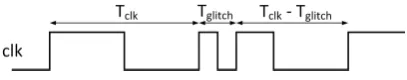
An adversary can cause setup time violation via clock glitches. Figure 1 shows the effect of a glitch on the clock signal. A clock glitch will temporarily shorten the clock cycle period fromTclktoTglitch, thereby causing timing violation of the
digital logic. When theglitch period(Tglitch) violates timing constraint of a path,
the output value of this path is captured before its computation is completed. Therefore, the captured value is very likely to be faulty.
2.2 Causes of Fault Bias
The fault behavior of a circuit under clock glitch injection is determined by its path delay distribution and the appliedfault intensity. For clock glitching, we define thefault intensity (FI)as the the inverse of glitch period,Tglitch (Fig. 1),
and quantify it with Equation 2. The following paragraphs explain how these two factors can be combined to inject biased faults.
F I= 1
Tglitch
(2)
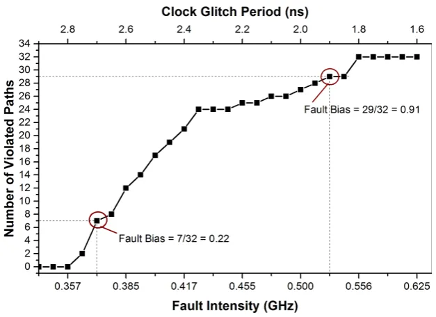
path delay distribution of the adder in the form of whisker plots. Each box-whisker plot in Figure 2(b) shows the delay distribution of paths within the fan-in cone of a different output bit. We extracted the path delays from a post-place-and-route netlist generated for a Xilinx Spartan 3E FPGA. As it is seen, the path delay distribution is non-uniform. For example, more than 50% of the path delays within the fan-in cone of bit Q3 are greater than all of the path delays within the fan-in cone of bitQ2. Similarly, the path delays within the fan-in cone ofQ0 are the smallest ones. This observation promises a biased (i.e, non-uniform) fault behavior. For example, it is possible to inject a fault that affects only a few bits of a targeted variable. This can be achieved by applying a fault intensity that violates only a few paths. If the applied fault intensity is greater than 0.364GHz (i.e,Tglitch>2.75ns), no faults can be injected into the ripple-carry
adder. However, single-bit faults can be injected on the bit Q3 when the fault
intensity is between 0.364GHz and 0.392GHz (i.e, 2.55ns < Tglitch <2.75ns).
Additional faults can be induced in the other bits only if the fault intensity value is increased further.
As a consequence, the non-uniform path delay distribution enables an adver-sary to obtain a biased fault behavior in proportion to the fault intensity. The next section provides a definition for the fault bias, which allows us to quantify it.
2.3 Quantifying Fault Bias
The fault bias is a property of the circuit architecture, which expose the poten-tial of a circuit to experience a setup time violation at a given fault intensity. Therefore, we can define the fault bias (FB) as the proportion of the violated paths for a given fault intensity. This definition enables us to quantify the fault bias as a number between 0 and 1 via Equation 3.
F B(f) =N umber of violated pathsN umber of all paths
F I=f (3)
Fig. 3.Number of violated paths with respect to the applied fault intensity and the corresponding glitch period for the ripple-carry adder.
Equation 3 reveals three important properties of fault bias. First, the fault bias is a property of circuit architecture. Therefore, an adversary can accurately model the fault behavior in terms of circuit architecture. Second, an adversary can control the severity of fault effects on a circuit by controlling the fault intensity. Higher fault intensity values induce more severe fault effects. Thus, each point in Figure 3 provides additional information that can be used as a source of leakage. Third, cryptographic hardware designers can evaluate the vulnerability of their designs to setup time time violation, and develop more efficient countermeasures. Next, we will demonstrate other parameters that affect the fault bias.
2.4 Effects of Operating Conditions and Data on Fault Bias
During an attack, the adversary can influence the dynamic path delay distri-bution throughthe input data andthe operating conditions. This will affect the fault bias. In the following paragraphs, we will demonstrate their effects on the path delays.
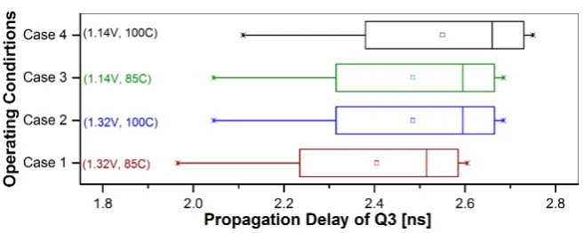
Fig. 4.The effect of varying the supply voltage and the operating temparature on the path delays. Increasing the temperature and decreasing the supply voltage increase the path delays.
path delays of the ripple carry adder. We investigate the path delay distribution within the fan-in cone of bit Q3 with four different (supply voltage, operating
temperature) combinations. We provide a separate box-whisker plot for each case. We obtained these data using Xilinx’s static timing analyzer tool.
The top two box-whisker plots of Figure 4 show the effect of increasing the operating temperature from 85C to 100C, while applying a constant supply voltage of 1.14V. The bottom two box-whisker plots show the same effect for the supply voltage of 1.32. As it is seen, the path delays increase with the increasing temperature.
TheCase 1 andCase 3 shows the effect of decreasing the supply voltage from 1.32V to 1.14V for a temperature of 85C. TheCase 2 andCase 4 illustrate the same effect for a temperature of 100C. As it is shown, the path delays increases with the decreasing supply voltage. These behaviors are compatible with the experimental results provided by Zussa et al. [12].
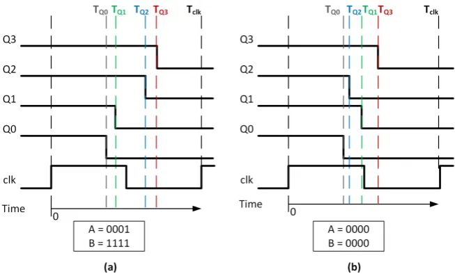
Effects of the Processed Data: An adversary can also influence the path delays via processed data since path delays are data-dependent.
In Figure 5, we provide post-place-and-route simulation results for our ripple-carry adder example to illustrate the data-dependency of its path delays. In the simulation, we first initialized the adder ouputs tologic-1. Then, we applied two different input sets and observed the timing of the output signals during their transition fromlogic-1 tologic-0. As it is seen, path delays have a distribution ofTQ3> TQ2> TQ1> TQ0for the first input set (Fig. 5(a)). The output bitQ3
settles down later than the other bits because of the ripple effect. On the other hand, the path delay distribution is TQ3 > TQ1 > TQ2 > TQ0 for the second
Fig. 5.Illustration of data-dependency of paths delays on the ripple-carry adder:(a)
TQ3> TQ2> TQ1> TQ0.(b)TQ3> TQ1> TQ2> TQ0.
3
Effects of Fault Bias on Circuit Behavior
In this section, we demonstrate the different effects of the fault bias on the circuit behavior, which are exploited by FSA, NUEVA, NUFVA, and DFIA. For this purpose, we provide some experimental results for two AES SBOX designs, namely, PPRM1-SBOX [13] and Comp-SBOX [14]. PPRM1-SBOX is a low-power SBOX design, which is based on a AND-XOR logic array. Comp-SBOX is a compact composite-field-based design, which decomposes the SBOX operation into smaller, lower-level finite-field operations.
Before proceeding further, we need the following definitions. We can model the effects of the fault injection on the targeted signal with an XOR operation:
s∗=s⊕e (4)
In Equation 4, thecorrect value,s, is the value of the targeted signal without fault injection. Thefaulty value,s∗, is the value of the targeted signal after fault injection. Theerror value,e, denotes the value of the injected fault itself. Ifi-th bit of the error value (e) is 1, thei-th bit of the correct value (s) is flipped and the faulty value (s∗) is obtained. Next, we will show different effects of fault bias on these values.
Fig. 6.The relationship between the critical timing delay and the Hamming weight of the input of PPRM1-SBOX [15].
time violation, the critical path delay determines the fault sensitivity point. As the path delay distribution of a circuit is data-dependent, the fault sensitivity of the circuit is also data-dependent.
Ghalaty et al. experimentally demonstrated this effect on an FPGA imple-mentation of PPRM1-SBOX architecture [15]. They obtained critical path delay value for each possible SBOX input in their experiment, where the initial values of SBOX outputs are logic-0. Figure 6 shows their critical path delay results with respect to the Hamming weight of the SBOX input values. As it is seen, the critical path delay of PPRM1-SBOX is proportional to the Hamming weight of the SBOX inputs.
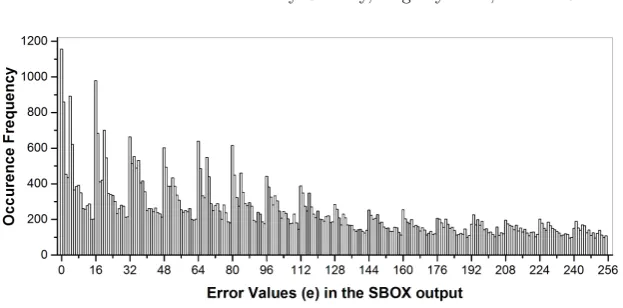
Non-uniform Error Value Distribution: Fault bias can also cause a non-uniform distribution in the error value (i.e, fault pattern).
Fig. 7. The distribution of injected error values in the output of PPRM1-SBOX (F ault Intensity= 0.238GHz).
Fig. 8. The distribution of faulty values in the output of Comp-SBOX (F ault Intensity= 0.250GHz).
is seen, the fault bias causes a non-uniform error value distribution. Also, error values that have low Hamming-weight are more likely to occur for this fault intensity value.
Non-uniform Faulty Value Distribution: Fault bias might also cause a non-uniform distribution in faulty values. By controlling the fault intensity, an adversary can make a circuit produce some faulty values more than the other faulty values.
sim-Fig. 9.The relationship between the critical timing delay and the Hamming weight of the input of PPRM1-SBOX [10]
.
ulation. The figure shows the distribution of faulty SBOX output values. The horizontal axis shows the faulty output values and the vertical axis shows the their frequency of occurrence. It also shows the distribution of fault-free SBOX output values. As it is shown (blue line of Fig. 8), the correct outputs of the SBOX have a uniform distribution. However, faulty outputs have a non-uniform distribution, and we see the output value 99 more than the other faulty values because of fault bias. This effect also experimentally demonstrated on an ASIC implementation of Comp-SBOX by Li et al. [16].
Small Changes in Fault Behavior: The effects of fault bias on a circuit’s operation has also a differential character: A small change in the fault intensity will cause a small change in the fault bias. Therefore, an adversary can gradually increase the number of induced faults by gradually increasing the fault intensity. This enables the adversary to combine the information obtained at different fault intensities.
Ghalaty et al. experimentally demonstrated this effect on an FPGA imple-mentation of PPRM1-SBOX architecture [10]. In their experiment, they col-lected the faulty SBOX output values, generated by a certain SBOX input value for 33 different clock frequencies. Figure 9 shows the number of faulty output bits, which they observed in the experiment, with respect to the applied clock frequency (i.e, fault intensity). As it is seen, the number of faulty output bits increases with the increasing fault intensity. As a consequence, this figure ex-perimentally demonstrates the gradual fault behavior in proportion to the fault intensity.
Fig. 10.Generic Fault Attack Framework
4
Building a Biased Fault Attack
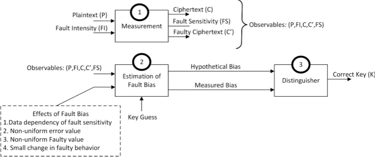
In the previous sections, we discussed a systematic description of fault bias, its causes and effects on the circuit behavior. In this section, we describe a generic framework for a systematic comparison of the fault attacks. Following are the steps of a fault attack. These steps are shown in Figure 10 as well.
– Step 1: Measurement: In this step, the adversary applies several plain-texts and all possible fault intensities to inject biased fault into the block cipher. Then, he collects the observables, namely, plaintexts, faulty cipher-texts, correct ciphertexts and fault intensities for further analysis. The col-lected observables contain fault bias information of the circuit.
– Step 2: Estimating the Effects of Fault Bias on Secret Intermediate Variable: The target of biased fault injection is a secret intermediate vari-able. Therefore, an adversary should first invert the observables back to the intermediate variables using key guesses. Then, the adversary estimates the effect of fault bias on hypothesized intermediate variable. Since the effects of fault bias are different, each attack strategy requires a different estimation function on the intermediate variable.
– Step 3: Distinguisher: Only for the correct key guess, the estimated fault bias values in Step 2 correspond to the observed fault bias in Step 1. In this step, we distinguish the correct key guess from the wrong key guesses. For this purpose, the distinguisher first assigns a number for the strength of the correlation between the collected observables (Step 1) and the fault bias estimations (Step 2). Then, it selects the key guess which corresponds to the maximum strength.
5
Biased Fault Attacks
Fig. 11.AES Structure
5.1 Advanced Encryption Standard Algorithm
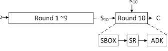
This section provides some preliminary information about AES algorithm and the notations used throughout this section. The AES algorithm consists of 10 rounds. The first 9 rounds have 4 main operations, SBOX, ShiftRows(SR), Mix-Column(MC) and AddRoundKey(ADK). Round 10 omits the MixColumn op-eration. Figure 11 shows the structure of the AES algorithm. In this figure,P is the applied plaintext to the AES algorithm, S10 is the intermediate state
vari-able for round 10.K10is the key for round 10 and Crepresents the ciphertext.
The faulty value of the variablexis shown byx0, x00, ....
All of the considered attacks aim at retrieving the last round key (K10).
However, the target round for fault injection might differ based on the attack strategy. Next, we will give the details of each attack.
5.2 Fault Sensitivity Analysis (FSA)
Fault Sensitivity Analysis (FSA) attack is proposed by Li et. al, in CHES 2010 [7]. Realizing that fault bias can have a data dependency on a secret value in a circuit, Li used it to demonstrate a fault attack with side-channel-like prop-erties. The steps of FSA are as below.
– Step 1: In this attack, the target of the fault injection is round 10. The observables are plaintext, ciphertext and fault sensitivity points.
– Step 2: For FSA, the effect of fault bias is the data dependency of fault sensitivity. The adversary first inverts the ciphertext to round 10 input (S10)
using a key guess. Then, he estimates the effect of fault bias as the Hamming Weight of round 10 inputHW(S10).
– Step 3: In this step the attacker uses the Pearson Correlation Coefficient to find the key guess for which the fault sensitivity is strongly correlated to
HW(S10) for all inputs.
5.3 Non-Uniform Error Value Analysis (NUEVA)
5.4 Non-Uniform Faulty Value Attack (NUFVA)
Fuhr generalized the NUEVA technique, by directly considering the distribution of the faulty secret variable separately. His technique therefore is called Non Uniform Faulty Value Analysis (NUFVA), to indicate that the bias is present in the fault value itself, rather than in the error pattern [9]. He also proposed sev-eral distinguisher techniques. The NUFVA attack can be performed in different rounds of AES including round 7, 8 and 9.
– Step 1: We take the round 9 as the fault injection target. Since, this attack is a faulty ciphertext only attack, the observables include the fault intensity and the faulty ciphertext.
– Step 2: The effect of fault bias for NUFVA is the non-uniform faulty value distribution. To extract the fault bias, the attacker must estimate the effect of fault bias on the faulty value. Therefore, he inverts the faulty ciphertext using a key hypothesis and obtain faulty inputs for round 10 (S100 ).
– Step 3: Using the values of faulty intermediate state, the attacker computes the distribution of faulty values for each key guess. Then, for each key guess, the attacker applies the Maximum likelihood function to distinguish the correct key guess from the wrong ones.
5.5 Differential Fault Intensity Analysis (DFIA)
The fourth technique that builds on fault analysis is Differential Fault Intensity Analysis (DFIA), proposed by Ghalaty [10]. The steps and properties of the attack are explained in the following steps.
Fig. 12. (a) Block diagram for the experimental setup.(b) Timing diagram for the experimental setup.
inverting the faulty ciphertexts and key guess for several fault intensity lev-els. Then, he computes the distance between the hypothesized intermediate variables by using the Hamming Distance function.
– Step 3: The fault bias assumption for DFIA enables the use of a distinguisher that looks for the smallest change. Unlike the previous techniques, DFIA can combine fault behaviors collected at multiple fault intensities. Hence, the complete fault bias characteristic of a circuit can be exploited. Based on the assumption of fault attack, the error values are close to each other for the correct key guess. For wrong key guesses, the distance between injected error values will be random due to the non-uniform behavior of the Sbox module. Therefore, the distinguisher function simply chooses the key that shows the minimal distance between intermediate variables.
6
Experimental Setup
In this work, we injected biased faults into a device under test (DUT) through gate-level simulation. As the DUT, we use two AES-128 designs: PPRM1-SBOX-based AES-128 (PPRM1-AES) and Comp-SBOX-PPRM1-SBOX-based AES-128 (Comp-AES). We generated the gate-level netlists of these designs for a Xilinx Spartan6 FPGA (45nmtechnology). Both DUTs compute each round of AES in a separate clock cycle. We use clock glitches as the fault injection means (Fig. 12(a)). This method generates a clock signal for the circuit as a combination of two clock signals, namely, glitch clock (clk g) and nominal clock (clk o). As it is seen in Fig-ure 12(b), we inject glitches in the clk o via anenable signal (g en). To inject a biased fault in the input of ther-th round of AES, we set theg ensignal just be-fore the clock cycle, in which ther-th round is computed. Such a glitch injection makes some timing paths fail during (r−1)-th roundand causes a biased fault in the input ofr-th round. We control the fault intensity by increasing/decreasing the period of theclk g signal.
In the second condition, we assume that the fault injection is in a noisy environment or the adversary is not able to control the timing of the glitch injection precisely [17]. Some previous works show that in case of using other injection tools such as Electromagnetic pulse injection, the attacker might not be able to specifically inject fault into one round [17]. In this case, we assume that the faults might occur in other rounds of the AES algorithm. In this case, we randomly choose the faulty results from several rounds of AES and study the effect of noise in the performance of the attacks.
7.1 Results for Ideal Fault Injection
In the ideal condition, we assume that the fault injection tool is based on the clock glitching and the attacker is able to identify the location of the fault in the AES algorithm. Based on the requirements of the discussed attacks, we inject faults in Round 9 for DFIA, NUEVA and NUFVA, and in round 10 for the FSA algorithm, in order to retrieve the key of the last round. Figure 13 shows the results of applying different attack strategies on two implementations of AES algorithm (PPRM1-AES and Comp-AES).
The first fault injection strategy is by starting from the correct ciphertext. Then, we gradually increase the fault intensity until we observe the first faulty ciphertext at the fault sensitivity point. We captured the faulty ciphertext with this method for 1000 plaintext. Then, we applied four attack strategies to the set of faulty ciphertexts. The results in Figure 13(a) and 13(b) show the required number of plaintext for retrieving the key. In this case, the required number of plaintexts simply shows the number of fault injection attempts, since there s one fault sensitivity point for each plaintext. As shown, in this case, even if we do not have multiple fault intensities, the DFIA attack works with less number of plaintexts compared to FSA and NUEVA. The NUFVA attack is not able to retrieve all bytes of the key as observing stuck-at or biased faulty value with this method of fault injection is very difficult.
(a) PPRM1 AES
(b) Comp AES
(c) PPRM1 AES
(d) Comp AES
only retrieve less than 5 bytes of the key. The reason is that we cannot observe biased faulty output or stuck-at faults in the intermediate state.
7.2 Results for Noisy Fault Injection
Assuming a noisy fault injection environment, we injected faults into round 6, 7, 8, 9 and 10. Then, as the set of faulty values, we choose faults from each round randomly. Then, we apply the four fault attacks, and count the number of fault injection attempts it requires to find the key. Figure 14(a) and 14(b) shows the number of required fault injections for each case. Since NUFVA attack cannot fully retrieve the key, the number of fault injection attempts shown is for the maximum number of key bytes that it can retrieve. As shown, DFIA is able to retrieve the key by less number of attempts compared to other attacks. The number of fault injection attempts increases exponentially for FSA attack. The reason is that due to the noise in the induced fault, the fault sensitivity point associated with each plaintext is for the data of the noisy rounds, rather than round 10. The NUEVA attack, is still successful when the noise is in round 8, however, in the last case, NUEVA can only retrieve 9 bytes of the key using all available plaintexts.
Since, NUFVA is not able to fully retrieve the key, to provide a fair compar-ison of the attacks, Figure 14(d) and 14(d) show the number of required fault injection attempts to retrieve only one byte of the key. As shown in these fig-ures, the required number of attempts for DFIA is much less compared to other attacks.
7.3 Attack Efficiency
In this section, we intend to compare the efficiency of the biased fault based at-tacks. The cost of an attack can be defined by the number of fault injections and the number of applied plaintexts used for the attack. As mentioned in previous sections, for each applied plaintext, we count the number of useful fault injection attempts. The attack efficiency in this paper is defined with the Equation 5.
(a) PPRM1 AES
(b) Comp AES
(c) PPRM1 AES
(d) Comp AES
that we injected fault only in the target location and second is the noisy condition in which we injected the fault in rounds 8, 9 and 10. Table 1 shows the efficiency of different fault attacks, in these two conditions for two implementations of AES. Since, NUFVA cannot completely retrieve the key, we provided the minimum number of fault injection attempts that it uses for partial key retrieval. Based on the results, DFIA needs less number of fault injection attempts compared to other attacks. The reason is that, the assumption on the effects of fault bias for the DFIA attack benefits from combining multiple fault intensity levels per plaintext. This property maximizes the information we can obtain from each biased fault injection and hence, helps to improve the efficiency of the DFIA attack.
8
Conclusion
Acknowledgment This research was supported through the National Science Foundation Grant 1441710, Grant 1115839, and through the Semiconductor Re-search Corporation.
References
1. Joye, M., Tunstall, M., eds.: Fault Analysis in Cryptography. Information Security and Cryptography. Springer Berlin Heidelberg (2012)
2. Karaklajic, D., Schmidt, J.M., Verbauwhede, I.: Hardware Designer’s Guide to Fault Attacks. Very Large Scale Integration (VLSI) Systems, IEEE Transactions on21(2013) 2295–2306
3. Barenghi, A., Bertoni, G., Parrinello, E., Pelosi, G.: Low Voltage Fault Attacks on the RSA Cryptosystem. In: IEEE Workshop on Fault Diagnosis and Tolerance in Cryptography (FDTC),, IEEE (2009) 23–31
4. Hutter, M., Schmidt, J.: The Temperature Side Channel and Heating Fault At-tacks. In: Smart Card Research and Advanced Applications - 12th International Conference, CARDIS 2013, Berlin, Germany, November 27-29, 2013. Revised Se-lected Papers. (2013) 219–235
5. van Woudenberg, J., Witteman, M., Menarini, F.: Practical Optical Fault Injection on Secure Microcontrollers. In: IEEE Workshop on Fault Diagnosis and Tolerance in Cryptography (FDTC),. (2011) 91–99
6. Clavier, C.: Attacking block ciphers. In Joye, M., Tunstall, M., eds.: Fault Anal-ysis in Cryptography. Information Security and Cryptography. Springer Berlin Heidelberg (2012) 19–35
7. Li, Y., Sakiyama, K., Gomisawa, S., Fukunaga, T., Takahashi, J., Ohta, K.: Fault Sensitivity Analysis. In: Cryptographic Hardware and Embedded Systems, CHES 2010. Springer (2010) 320–334
8. Lashermes, R., Reymond, G., Dutertre, J., Fournier, J., Robisson, B., Tria, A.: A DFA on AES Based on the Entropy of Error Distributions. In: IEEE Workshop on Fault Diagnosis and Tolerance in Cryptography (FDTC),, IEEE (2012) 34–43 9. Fuhr, T., Jaulmes, E., Lomn´e, V., Thillard, A.: Fault Attacks on AES with Faulty
Ciphertexts Only. In: IEEE Workshop on Fault Diagnosis and Tolerance in Cryp-tography (FDTC),, IEEE (2013) 108–118
10. Ghalaty, N.F., Yuce, B., Taha, M., Schaumont, P.: Differential fault intensity analysis. In: IEEE Workshop on Fault Diagnosis and Tolerance in Cryptography (FDTC),, IEEE (2014) 49–58
11. Agoyan, M., Dutertre, J.M., Naccache, D., Robisson, B., Tria, A.: When Clocks Fail: On Critical Paths and Clock Faults. In: Smart Card Research and Advanced Application. Springer (2010) 182–193
12. Zussa, L., Dutertre, J.m., Cl´ediere, J., Robisson, B., Tria, A.: Investigation of Timing Constraints Violation as a Fault Injection Means. In: 27th Conference on Design of Circuits and Integrated Systems (DCIS). (2012)
13. Morioka, S., Satoh, A.: An Optimized S-Box Circuit Architecture for Low Power AES Design. In: Cryptographic Hardware and Embedded Systems-CHES 2002. Springer (2003) 172–186

![Fig. 6. The relationship between the critical timing delay and the Hamming weight ofthe input of PPRM1-SBOX [15].](https://thumb-us.123doks.com/thumbv2/123dok_us/7930398.1316809/9.595.163.440.130.339/relationship-critical-timing-delay-hamming-weight-ofthe-input.webp)
![Fig. 9. The relationship between the critical timing delay and the Hamming weight ofthe input of PPRM1-SBOX [10]](https://thumb-us.123doks.com/thumbv2/123dok_us/7930398.1316809/11.595.145.475.104.238/relationship-critical-timing-delay-hamming-weight-ofthe-input.webp)