Supertex inc.
HV857
Features
► Patented audible noise reduction ► Patented lamp aging compensation
► 190 VPP output voltage for higher brightness ► Patented output timing for high efficiency
► Single cell lithium ion compatible ► 150nA shutdown current
► Wide input voltage range 1.8 to 5.0V ► Separately adjustable lamp and converter
frequencies
► Output voltage regulation ► Split supply capability
► Available in 8-Lead MSOP and DFN packages
Applications
► LCD backlighting ► Mobile Cellular Phone ► PDAs
► Handheld wireless communication products ► Global Positioning Systems (GPS)
General Description
The Supertex HV857 is a high voltage driver designed for driving
Electroluminescent (EL) lamps of up to 5.0 square inches. The input supply voltage range is from 1.8 to 5.0V. The device uses
a single inductor and a minimum number of passive components. The nominal regulated output voltage that is applied to the EL
lamp is ±95V. The chip can be enabled/disabled by connecting the
resistor on RSW-Osc to VDD/GND.
The HV857 has two internal oscillators, a switching MOSFET, and
a high voltage EL lamp driver. The frequency for the switching MOSFET is set by an external resistor connected between the RSW-Osc pin and the supply pin VDD. The EL lamp driver frequency is set by an external resistor connected between
REL-Osc pin and VDD pin. An external inductor is connected between the LX and VDD pins or VIN for split supply applications. A
0.003-0.1µF capacitor is connected between CS and ground. The EL lamp is connected between VA and VB.
The switching MOSFET charges the external inductor and discharges it into the capacitor at CS. The voltage at CS will start to increase. Once the voltage at CS reaches a nominal value of 95V, the switching MOSFET is turned OFF to conserve power. The
outputs VA and VB are configured as an H bridge and are switching
in opposite states to achieve ±95V across the EL lamp.
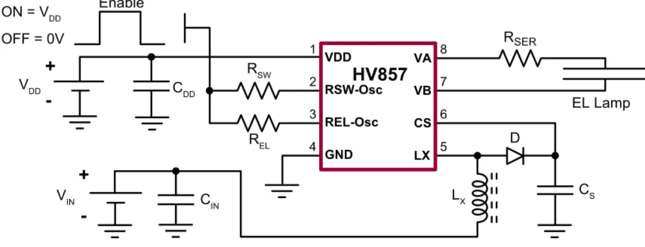
Typical Application Circuit
Low Noise, High Voltage
EL Lamp Driver IC
EL Lamp+
_
CS VIN LX CIN Enable Signal ON = VDD OFF = 0 D+
_
VDD C DD RSW REL 1 2 3 4 8 7 6 5 VDD RSW-Osc REL-Osc GND VA VB CS LXHV857
HV857
Absolute Maximum Ratings
Parameter Value
Supply voltage, VDD -0.5V to 6.5V Operating temperature -40°C to +85°C
Storage temperature -65°C to +150°C
DFN-8 power dissipation 1.6W
MSOP-8 power dissipation 300mW
Output voltage, VCS -0.5 to +120V
Absolute Maximum Ratings are those values beyond which damage to the device may occur. Functional operation under these conditions is not im-plied. Continuous operation of the device at the absolute rating level may affect device reliability. All voltages are referenced to device ground.
Pin Configuration
8-Lead MSOP (top view) Pads are at the bottom of the package.
Exposed center pad is at ground potential. 8-Lead DFN (top view) 1 2 3 4 8 7 6 5 VDD RSW-Osc REL-Osc GND VA VB CS LX 1 2 3 4 8 7 6 5 VDD RSW-Osc REL-Osc GND VA VB CS LX
Typical Thermal Resistance
Package θja
8-Lead DFN 37OC/W
8-Lead MSOP 171OC/W
Mounted on FR4 board, 25mm x 25mm x 1.57mm
Sym Parameter Min Typ Max Units Conditions
VDD Supply voltage 1.8 - 5.0 V
---fEL Operating drive frequency - - 1.0 kHz
---TA Operating temperature -40 - +85 OC
---Recommended Operating Conditions
Sym Parameter Min Typ Max Units Conditions
EN-L Logic input low voltage 0 - 0.2 V VDD = 1.8 to 5.0V
EN-H Logic input high voltage VDD - 0.2 - VDD V VDD = 1.8 to 5.0V
Enable/Disable Function Table
Sym Parameter Min Typ Max Units Conditions
RDS(ON) On-resistance of switching transistor - - 6.0 Ω I = 100mA
VCS Max. output regulation voltage 85 95 105 V VDD=1.8 to 5.0V
DC Electrical Characteristics
(Over recommended operating conditions unless otherwise specified, TA = 25°C)Product Marking
H857
Y W L L
Y = Last Digit of Year Sealed W = Code for Week Sealed L = Lot Number = “Green” Packaging L = Lot Number YY = Year Sealed WW = Week Sealed = “Green” Packaging H857 LLLL YYWW Top Marking Bottom Marking 8-Lead DFN 8-Lead MSOP
Package may or may not include the following marks: Si or
Package may or may not include the following marks: Si or
Ordering Information
Part Number Package Packing
HV857K7-G 8-Lead DFN 3000/Reel
HV857MG-G 8-Lead MSOP 2500/Reel
HV857
Block Diagram
* The inductor used is a 220µH Murata inductor, max DC resistance of 8.4Ω, part # LQH32CN221K21.
Figure 1: Typical Application/ Test Circuit
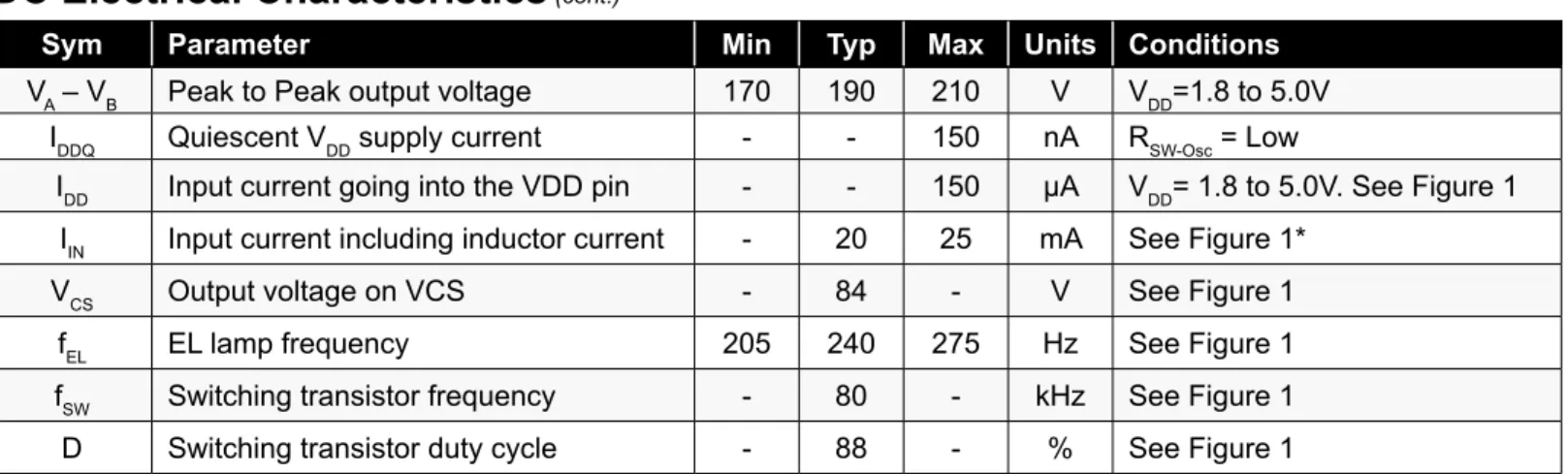
DC Electrical Characteristics
(cont.)Sym Parameter Min Typ Max Units Conditions
VA – VB Peak to Peak output voltage 170 190 210 V VDD=1.8 to 5.0V IDDQ Quiescent VDD supply current - - 150 nA RSW-Osc = Low
IDD Input current going into the VDD pin - - 150 µA VDD= 1.8 to 5.0V. See Figure 1 IIN Input current including inductor current - 20 25 mA See Figure 1*
VCS Output voltage on VCS - 84 - V See Figure 1
fEL EL lamp frequency 205 240 275 Hz See Figure 1 fSW Switching transistor frequency - 80 - kHz See Figure 1 D Switching transistor duty cycle - 88 - % See Figure 1
C + _ VREF Disable High Voltage Level Translator GND VDD Q Q Q VA CS LX VB Q RSW-Osc REL-Osc VSENSE EL Osc VDD Switch Osc 220µH* 3.3nF 100V 560kΩ 2.0MΩ BAS21 * Murata Inductor LQH32CN221K21
HV857
ON = VDD OFF = 0V Enable Signal + - V IN 4.7µF + - V DD 0.1µF2.0kΩ Equivalent to 3.0in2 lamp 10nF 1 2 3 4 8 7 6 5 VDD RSW-Osc REL-Osc GND VA VB CS LX HV857
HV857
Typical Performance
Device Lamp Size VDD = VIN IIN VCS fEL Brightness
HV857MG-G 3.0in2 3.3V 20.0mA 84V 240Hz 6.0ft-lm
Typical Performance Curves for Figure 1
(EL Lamp = 3.0in2, VDD = 3.0V)
IIN, VCS, Brightness vs Inductor Value
0 10 20 30 40 50 60 70 80 90 100 100 200 300 400 500 600 Inductor Value (µH) 0 1 2 3 4 5 6 7 Brightness VCS IIN vs VIN 13 15 17 19 21 23 25 VIN (V) VCS (V) lIN (mA) Brightness (ft-lm) lIN (mA) lIN (mA), VCS (V) Brightness (ft-Im) Brightness vs VIN 1 2 3 4 5 6 7 1.5 2.5 3.5 4.5 5.5 VIN (V) IIN vs VCS 14 16 18 20 22 24 55 65 75 85 95 VCS (V) VCS vs VIN 55 65 75 85 95 VIN (V) lIN 1.5 2.5 3.5 4.5 5.5 1.5 2.5 3.5 4.5 5.5
HV857
External Component Description
External
Component Description
Diode Fast reverse recovery diode, BAS21 diode or equivalent.
CS Capacitor 0.003µF to 0.1µF, 100V capacitor to GND is used to store the energy transferred from the inductor.
REL Resistor
The EL lamp frequency is controlled via an external REL resistor connected between REL-Osc and VDD
of the device. The lamp frequency increases as REL decreases. As the EL lamp frequency increases, the amount of current drawn from the battery will increase and the output voltage VCS will decrease. The
color of the EL lamp is dependent upon its frequency.
A 2MΩ resistor would provide lamp frequency of 205 to 275Hz. Decreasing the REL resistor by a factor of 2 will increase the lamp frequency by a factor of 2.
fEL = (2MΩ)(240Hz) REL
RSW Resistor
The switching frequency of the converter is controlled via an external resistor, RSW between RSW-Osc
and VDD of the device. The switching frequency increases as RSW decreases. With a given inductor, as
the switching frequency increases, the amount of current drawn from the battery will decrease and the
output voltage, VCS, will also decrease.
fSW = (560kΩ)(80Hz) RSW
LX Inductor
The inductor LX is used to boost the low input voltage by inductive flyback. When the internal switch is
on, the inductor is being charged. When the internal switch is off, the charge stored in the inductor will be transferred to the high voltage capacitor CS. The energy stored in the capacitor is connected to the
internal H-bridge, and therefore to the EL lamp. In general, smaller value inductors, which can handle more current, are more suitable to drive larger size lamps. As the inductor value decreases, the
switch-ing frequency of the inductor (controlled by RSW) should be increased to avoid saturation.
A 220µH Murata (LQH32CN221) inductor with 8.4Ω series DC resistance is typically recommended. For
inductors with the same inductance value, but with lower series DC resistance, lower RSW resistor value is needed to prevent high current draw and inductor saturation.
Lamp
As the EL lamp size increases, more current will be drawn from the battery to maintain high voltage across the EL lamp. The input power, (VIN x IIN), will also increase. If the input power is greater than
the power dissipation of the package, an external resistor in series with one side of the lamp is recom-mended to help reduce the package power dissipation.
HV857
Split Supply Configuration
The HV857 can also be used for handheld devices operating
from a battery where a regulated voltage is available. This
is shown in Figure 2. The regulated voltage can be used to run the internal logic of the HV857. The amount of current
necessary to run the internal logic is 150µA Max at a VDD of
3.0V. Therefore, the regulated voltage could easily provide
the current without being loaded down.
The HV857 can be easily enabled and disabled via a logic
control signal on the RSW and REL resistors as shown in Fig-ure 2 below. The control signal can be from a microproces-sor. The control signal has to track the VDD supply. RSW and REL are typically very high values. Therefore, only 10’s of
microamperes will be drawn from the logic signal when it
is at a logic high (enable) state. When the microprocessor
signal is high the device is enabled, and when the signal is low, it is disabled.
Enable/Disable Configuration
Figure 2: Split Supply and Enable/Disable Configuration
Audible Noise Reduction
This section describes a method (patented) developed at Supertex to reduce the audible noise emitted by the EL
lamps used in application sensitive to audible noise. Figure
3 shows a general circuit schematic that uses the resistor,
RSER, connected in series with the EL lamp.
EL Lamp ON = VDD
OFF = 0V Enable Signal
LX CS Regulated Voltage = VDD CIN D REL RSW CDD VIN + - 1 2 3 4 8 7 6 5 VDD RSW-Osc REL-Osc GND VA VB CS LX
HV857
Figure 3: Typical Application Circuit for Audible Noise Reduction
1 2 3 4 8 7 6 5
HV857
EL Lamp ON = VDD OFF = 0V Enable LX CS+
-
VIN C IN D REL RSW+
-
VDD CDD RSER VDD RSW-Osc REL-Osc GND VA VB CS LXHV857
Minimization of EL Lamp Audible Noise
The EL lamp, when lit, emits an audible noise. This is due
to EL lamp construction and it creates a major problem for
applications where the EL lamp can be close to the ear such as cellular phones. The noisiest waveform is a square wave and the quietest waveform has been assumed to be a sine wave.
After extensive research, Supertex has developed a wave-form that is quieter than a sine wave. The wavewave-form takes
the shape of approximately 2RC time constants for rising
and 2RC time constants for falling, where C is the capaci-tance of the EL lamp, and R is the external resistor, RSER, connected in series with the EL lamp. This waveform has been proven to generate less noise than a sine wave. The audible noise from the EL lamp can be set at a desired level based on the series resistor value used with the lamp. It is important to note that use of this resistor will reduce the voltage across the lamp. Reduction of voltage across the lamp will also have another effect on the over all per-formance of the Supertex EL drivers, age compensation
(patented). This addresses a very important issue, EL lamp
life that most mobile phone manufacturers are concerned about.
Effect of Series Resistor on EL Lamp
Audible Noise and Brightness
As EL lamp ages, its brightness is reduced and its
capaci-tance is diminished. By using the RC model to reduce the audible noise emitted by the EL lamp, the voltage across the
lamp will increase as its capacitance diminishes. Hence the increase in voltage will compensate for the reduction of the
brightness. As a result, it will extend the EL lamp’s half-life (half the original brightness).
Increasing the value of the series resistor with the lamp will reduce the EL lamp audible noise as well as its brightness. This is due to the fact that the output voltage across the lamp will be reduced and the output waveform will have rounder edges.
HV857
8-Lead DFN Package Outline (K7)
3.00x3.00mm body, 0.80mm height (max), 0.65mm pitch
Symbol A A1 A3 b D D2 E E2 e L L1 θ Dimension (mm) MIN 0.70 0.00 0.20 REF 0.25 2.85* 1.60 2.85* 1.35 0.65 BSC 0.30 0.00* 0O NOM 0.75 0.02 0.30 3.00 - 3.00 - 0.40 - -MAX 0.80 0.05 0.35 3.15* 2.50 3.15* 1.75 0.50 0.15 14O JEDEC Registration MO-229, Variation WEEC-2, Issue C, Aug. 2003.
* This dimension is not specified in the JEDEC drawing. Drawings not to scale.
Supertex Doc. #: DSPD-8DFNK73X3P065, Version C081109.
Seating Plane θ
Top View
Bottom View
A A1 D E D2 E2 A3 L L1 View B Note 1 (Index Area D/2 x E/2) Note 3 Note 2 Note 1 (Index Area D/2 x E/2) 1 1 8 8 e b
Side View
View B
Notes:
1. A Pin 1 identifier must be located in the index area indicated. The Pin 1 identifier can be: a molded mark/identifier; an embedded metal marker; or
a printed indicator.
2. Depending on the method of manufacturing, a maximum of 0.15mm pullback (L1) may be present.
Supertex inc. does not recommend the use of its products in life support applications, and will not knowingly sell them for use in such applications unless it receives an adequate “product liability indemnification insurance agreement.” Supertex inc. does not assume responsibility for use of devices described, and limits its liability to the replacement of the devices determined defective due to workmanship. No responsibility is assumed for possible omissions and inaccuracies. Circuitry and specifications are subject to change without notice. For the latest product specifications refer to the Supertex inc. (website: http//www.supertex.com)
HV857
(The package drawing(s) in this data sheet may not reflect the most current specifications. For the latest package outline information go to http://www.supertex.com/packaging.html.)
8-Lead MSOP Package Outline (MG)
3.00x3.00mm body, 1.10mm height (max), 0.65mm pitch
View B
View A-A
Seating Plane Gauge Plane L L1 L2View B
θ1 θ 1 8 E E1 D e b A A2 A1 Seating Plane A ATop View
Side View
Note 1 (Index Area D/2 x E1/2) Symbol A A1 A2 b D E E1 e L L1 L2 θ θ1 Dimension (mm) MIN 0.75* 0.00 0.75 0.22 2.80* 4.65* 2.80* 0.65 BSC 0.40 0.95 REF 0.25BSC 0O 5O NOM - - 0.85 - 3.00 4.90 3.00 0.60 - -MAX 1.10 0.15 0.95 0.38 3.20* 5.15* 3.20* 0.80 8O 15O JEDEC Registration MO-187, Variation AA, Issue E, Dec. 2004.* This dimension is not specified in the JEDEC drawing. Drawings are not to scale.
Supertex Doc. #: DSPD-8MSOPMG, Version H041309.
Note:
1. A Pin 1 identifier must be located in the index area indicated. The Pin 1 identifier can be: a molded mark/identifier; an embedded metal marker; or