1 FIGURE 1. Two-Pole Low-Pass Filter Using UAF42.
NOTE: A UAF42 and two external resistors make a unity-gain, two-pole, 1.25dB ripple Chebyshev low-pass filter. With the resistor values shown, cutoff frequency is 10kHz.
Although active filters are vital in modern electronics, their design and verification can be tedious and time consuming. To aid in the design of active filters, Burr-Brown provides a series of FilterPro™ computer-aided design programs. Us-ing the FILTER42 program and the UAF42 it is easy to design and implement all kinds of active filters. The UAF42 is a monolithic IC which contains the op amps, matched resistors, and precision capacitors needed for a state-variable filter pole-pair. A fourth, uncommitted precision op amp is also included on the die.
Filters implemented with the UAF42 are time-continuous, free from the switching noise and aliasing problems of switched-capacitor filters. Other advantages of the state-variable topology include low sensitivity of filter parameters to external component values and simultaneous low-pass, high-pass, and band-pass outputs. Simple two-pole filters can be made with a UAF42 and two external resistors—see Figure 1.
The DOS-compatible program guides you through the de-sign process and automatically calculates component values. Low-pass, high-pass, band-pass, and band-reject (or notch) filters can be designed.
Active filters are designed to approximate an ideal filter response. For example, an ideal low-pass filter completely
eliminates signals above the cutoff frequency (in the stop-band), and perfectly passes signals below it (in the pass-band). In real filters, various trade-offs are made in an attempt to approximate the ideal. Some filter types are optimized for gain flatness in the pass-band, some trade-off gain variation or ripple in the pass-band for a steeper rate of attenuation between the pass-band and stop-band (in the transition-band), still others trade-off both flatness and rate of roll-off in favor of pulse-response fidelity. FILTER42 supports the three most commonly used all-pole filter types: Butterworth, Chebyshev, and Bessel. The less familiar In-verse Chebyshev is also supported. If a two-pole band-pass or notch filter is selected, the program defaults to a resonant-circuit response.
Butterworth (maximally flat magnitude). This filter has the flattest possible pass-band magnitude response. Attenuation is –3dB at the design cutoff frequency. Attenuation beyond the cutoff frequency is a moderately steep –20dB/decade/ pole. The pulse response of the Butterworth filter has mod-erate overshoot and ringing.
Chebyshev (equal ripple magnitude). (Other transliterations of the Russian Heby]ov are Tschebychev, Tschebyscheff or Tchevysheff). This filter response has steeper initial rate of attenuation beyond the cutoff frequency than Butterworth.
A1 R2 50kΩ A2 A3 R4 50kΩ UAF42 11 R1 50kΩ RF1 15.8kΩ RF2 15.8kΩ C1 1000pF C2 1000pF 13 8 7 14 2 VIN R3 50kΩ VO 1
FILTER DESIGN PROGRAM FOR
THE UAF42 UNIVERSAL ACTIVE FILTER
By Johnnie Molina and R. Mark Stitt (602) 746-7592
APPLICATION BULLETIN
®Mailing Address: PO Box 11400 • Tucson, AZ 85734 • Street Address: 6730 S. Tucson Blvd. • Tucson, AZ 85706 Tel: (602) 746-1111 • Twx: 910-952-111 • Telex: 066-6491 • FAX (602) 889-1510 • Immediate Product Info: (800) 548-6132
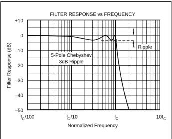
This advantage comes at the penalty of amplitude variation (ripple) in the pass-band. Unlike Butterworth and Bessel responses, which have 3dB attenuation at the cutoff quency, Chebyshev cutoff frequency is defined as the fre-quency at which the response falls below the ripple band. For even-order filters, all ripple is above the dc-normalized passband gain response, so cutoff is at 0dB (see Figure 2A). For odd-order filters, all ripple is below the dc-normalized passband gain response, so cutoff is at –(ripple) dB (see Figure 2B). For a given number of poles, a steeper cutoff can be achieved by allowing more pass-band ripple. The Chebyshev has more ringing in its pulse response than the Butterworth—especially for high-ripple designs.
Inverse Chebyshev (equal minima of attenuation in the stop band). As its name implies, this filter type is cousin to the
Chebyshev. The difference is that the ripple of the Inverse Chebyshev filter is confined to the stop-band. This filter type has a steep rate of roll-off and a flat magnitude response in the pass-band. Cutoff of the Inverse Chebyshev is defined as the frequency where the response first enters the specified stop-band—see Figure 3. Step response of the Inverse Chebyshev is similar to the Butterworth.
Bessel (maximally flat time delay), also called Thomson. Due to its linear phase response, this filter has excellent pulse response (minimal overshoot and ringing). For a given number of poles, its magnitude response is not as flat, nor is its initial rate of attenuation beyond the –3dB cutoff fre-quency as steep as the Butterworth. It takes a higher-order Bessel filter to give a magnitude response similar to a given Butterworth filter, but the pulse response fidelity of the Bessel filter may make the added complexity worthwhile. Tuned Circuit (resonant or tuned-circuit response). If a two-pole band-pass or band-reject (notch) filter is selected, the program defaults to a tuned circuit response. When band-pass response is selected, the filter design approximates the response of a series-connected LC circuit as shown in Figure 4A. When a two-pole band-reject (notch) response is se-lected, filter design approximates the response of a parallel-connected LC circuit as shown in Figure 4B.
CIRCUIT IMPLEMENTATION
In general, filters designed by this program are implemented with cascaded filter subcircuits. Subcircuits either have a two-pole (complex pole-pair) response or a single real-pole response. The program automatically selects the subcircuits required based on function and performance. A program option allows you to override the automatic topology selec-tion routine to specify either an inverting or noninverting pole-pair configuration.
FIGURE 3. Response vs Frequency for 5-pole, –60dB Stop-Band, Inverse Chebyshev Low-Pass Filter Showing Cutoff at –60dB.
FILTER RESPONSE vs FREQUENCY
Normalized Frequency f /100C f /10C f C 10f C +10 0 –10 –20 –30 –40 –50 Filter Response (dB) 5-Pole Chebyshev 3dB Ripple Ripple FILTER RESPONSE vs FREQUENCY
Normalized Frequency f /100C f /10C f C 10f C +10 0 –10 –20 –30 –40 –50 Filter Response (dB) 4-Pole Chebyshev 3dB Ripple Ripple
FIGURE 2A. Response vs Frequency for Even-Order (4-pole) 3dB Ripple Chebyshev Low-Pass Filter Showing Cutoff at 0dB.
FIGURE 2B. Response vs Frequency for Odd-Order (5-pole) 3dB Ripple Chebyshev Low-Pass Filter Showing Cutoff at –3dB.
FILTER RESPONSE vs FREQUENCY
fC/10 Normalized Frequency fC 10fC 100fC Normalized Gain (dB) 20 0 –20 –40 –60 –80 –100 AMIN fSTOPBAND
FIGURE 6. Multiple-Stage Filter Made with Two or More Subcircuits.
NOTES:
(1) Subcircuit will be a real-pole high-pass (HP), real-pole low-pass (LP), or complex pole-pair (PP1 through PP6) subcircuit specified on the UAF42 Filter Component Values and Filter Block Diagram program outputs.
(2) If the subcircuit is a pole-pair section, HP Out, BP Out, LP Out, or Aux Out will be specified on the UAF42 Filter Block Diagram program output. VIN VO Subcircuit N In Out(2) (1) Subcircuit 1 In Out(2) (1) NOTES:
(1) Subcircuit will be a complex pole-pair (PP1 through PP6) subcircuit specified on the UAF42 Filter Component Values and Filter Block Diagram program outputs.
(2) HP Out, BP Out, LP Out, or Aux Out will be specified on the UAF42 Filter Block Diagram program output.
VIN VO
Subcircuit 1
In Out(2)
(1)
FIGURE 5. Simple Filter Made with Single Complex Pole-Pair Subcircuit.
FIGURE 4B. n = 2 Band-Reject (Notch) Filter Using UAF42 (approximates the response of a par-allel-connected tuned L, C, R circuit). FIGURE 4A. n = 2 Band-Pass Filter Using UAF42
(ap-proximates the response of a series-connected tuned L, C, R circuit).
The simplest filter circuit consists of a single pole-pair subcircuit as shown in Figure 5. More complex filters consist of two or more cascaded subcircuits as shown in Figure 6. Even-order filters are implemented entirely with UAF42 pole-pair sections and normally require no external capacitors. Odd-order filters additionally require one real pole section which can be implemented with the fourth uncommitted op amp in the UAF42, an external resistor, and an external capacitor. The program can be used to design filters up to tenth order.
The program guides you through the filter design and gen-erates component values and a block diagram describing the filter circuit. The Filter Block Diagram program output shows the subcircuits needed to implement the filter design labeled by type and connected in the recommended order. The Filter Component Values program output shows the values of all external components needed to implement the filter. C L VIN VO R C L VIN VO R
SUMMARY OF FILTER TYPES
Butterworth
Advantages: Maximally flat magnitude
response in the pass-band. Good all-around performance. Pulse response better than Chebyshev.
Rate of attenuation better than Bessel.
Disadvantages: Some overshoot and ringing in
step response.
Chebyshev
Advantages: Better rate of attenuation
beyond the pass-band than Butterworth.
Disadvantages: Ripple in pass-band.
Considerably more ringing in step response than Butterworth.
Inverse Chebyshev
Advantages: Flat magnitude response in
pass-band with steep rate of attenuation in transition-band.
Disadvantages: Ripple in stop-band.
Some overshoot and ringing in step response.
Bessel
Advantages: Best step response—very little
overshoot or ringing.
Disadvantages: Slower initial rate of
attenua-tion beyond the pass-band than Butterworth.
At low frequencies, the value required for the frequency-setting resistors can be excessive. Resistor values above about 5MΩ can react with parasitic capacitance causing poor filter performance. When fO is below 10Hz, external
capacitors must be added to keep the value of RF1 and RF2
below 5MΩ . When fO is in the range of about 10Hz to 32Hz,
An external 5.49kΩ resistor, R2A, is added in parallel with
the internal resistor, R2, to reduce RF1 and RF2 by √10 and
eliminate the need for external capacitors. At the other extreme, when fO is above 10kHz, R2A, is added in parallel
with R2 to improve stability.
External filter gain-set resistors, RG, are always required
when using an inverting pole-pair configuration or when using a noninverting configuration with Q < 0.57.
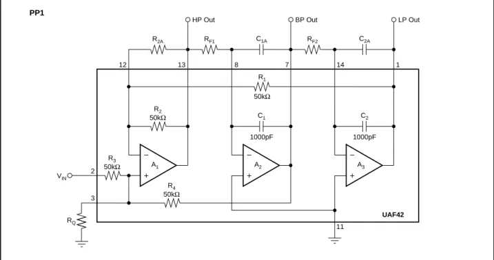
PP1 (Noninverting pole-pair subcircuit using internal gain-set resistor, R3)—See Figure 7. In the automatic topology
selection mode, this configuration is used for all band-pass filter responses. This configuration allows the combination of unity pass-band gain and high Q (up to 400). Since no external gain-set resistor is required, external parts count is minimized.
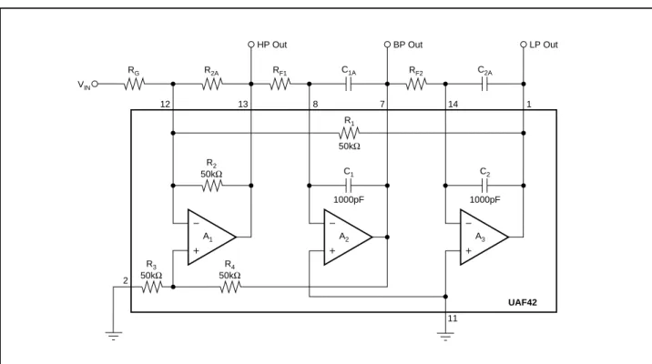
PP2 (Noninverting pole-pair subcircuit using an external gain-set resistor, RG)—See Figure 8. This configuration is
used when the pole-pair Q is less than 0.57.
PP3 (Inverting pole-pair subcircuit)—See Figure 9A. In the automatic topology selection mode, this configuration is used for the all-pole low-pass and high-pass filter responses. This configuration requires an external gain-set resistor, RG.
With RG = 50kΩ, low-pass and high-pass gain are unity.
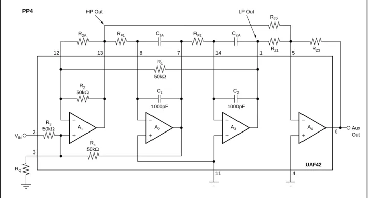
PP4 (Noninverting pole-pair/zero subcircuit)—See Figure 10. In addition to a complex pole-pair, this configuration produces a jω-axis zero (response null) by summing the low-pass and high-low-pass outputs using the auxiliary op amp, A4,
in the UAF42. In the automatic topology selection mode, this configuration is used for all band-reject (notch) filter responses and Inverse Chebyshev filter types when Q > 0.57. This subcircuit option keeps external parts count low by using the internal gain-set resistor, R3.
PP5 (Noninverting pole-pair/zero subcircuit)—See Figure 11. In addition to a complex pole-pair, this configuration produces a jω-axis zero (response null) by summing the low-pass and high-low-pass outputs using the auxiliary op amp, A4,
in the UAF42. In the automatic topology selection mode, this configuration is used for all band-reject (notch) filter responses and Inverse Chebyshev filter types when Q < 0.57. This subcircuit option requires an external gain-set resistor, RG.
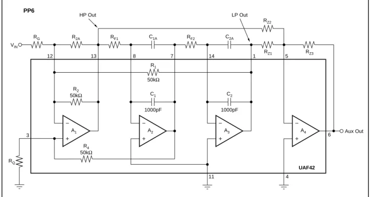
PP6 (Inverting pole-pair/zero subcircuit)—See Figure 12. In addition to a complex pole-pair, this configuration produces a jω-axis zero (response null) by summing the low-pass and high-pass outputs using the auxiliary op amp, A4, in the
UAF42. This subcircuit is only used when you override the automatic topology selection algorithm and specify the in-verting pole-pair topology. Then it is used for all band-reject (notch) filter responses and Inverse Chebyshev filter types. The program automatically places lower Q stages ahead of
higher Q stages to prevent op amp output saturation due to gain peaking. Even so, peaking may limit input voltage to less than ±10V (VS = ±15V). The maximum input voltage
for each filter design is shown on the filter block diagram. If the UAF42 is to be operated on reduced supplies, the maximum input voltage must be derated commensurately. To use the filter with higher input voltages, you can add an input attenuator.
The program designs the simplest filter that provides the desired AC transfer function with a pass-band gain of 1.0V/V. In some cases the program cannot make a unity-gain filter and the pass-band unity-gain will be less than 1.0V/V. In any case, overall filter gain is shown on the filter block diagram. If you want a different gain, you can add an additional stage for gain or attenuation as required. To build the filter, print-out the block diagram and compo-nent values. Consider one subcircuit at a time. Match the subcircuit type referenced on the component print-out to its corresponding circuit diagram—see the Filter Subcircuits section of this bulletin.
The UAF42 Filter Component Values print-out has places to display every possible external component needed for any subcircuit. Not all of these components will be required for any specific filter design. When no value is shown for a component, omit the component. For example, the detailed schematic diagrams for complex pole-pair subcircuits show external capacitors in parallel with the 1000pF capacitors in the UAF42. No external capacitors are required for filters above approximately 10Hz.
After the subcircuits have been implemented, connect them in series in the order shown on the filter block diagram.
FILTER SUBCIRCUITS
Filter designs consist of cascaded complex pole-pair and real-pole subcircuits. Complex pole pair subcircuits are based on the UAF42 state-variable filter topology. Six varia-tions of this circuit can be used, PP1 through PP6. Real pole sections can be implemented with the auxiliary op amp in the UAF42. High-pass (HP) and low-pass (LP) real-pole sections can be used. The subcircuits are referenced with a two or three letter abbreviation on the UAF42 Filter Compo-nent Values and Filter Block Diagram program outputs. Descriptions of each subcircuit follow:
POLE-PAIR (PP) SUBCIRCUITS
In general, all complex pole-pair subcircuits use the UAF42 in the state-variable configuration. The two filter parameters that must be set for the pole-pair are the filter Q and the natural frequency, fO. External resistors are used to set these
parameters. Two resistors, RF1 and RF2, must be used to set
the pole-pair fO. A third external resistor, RQ, is usually
FIGURE 7. PP1 Noninverting Pole-Pair Subcircuit Using Internal Gain-Set Resistor R3.
FIGURE 8. PP2 Noninverting Pole-Pair Subcircuit Using External Gain-Set Resistor RG.
PP1 PP2 A1 R2 50kΩ A2 A3 R3 50kΩ R4 50kΩ UAF42 11 R1 50kΩ RF1 RF2 C1 1000pF C2 1000pF VIN 2 13 8 7 14 3 RQ R2A C1A C2A LP Out BP Out HP Out 1 12 A1 R2 50kΩ A2 A3 R4 50kΩ UAF42 11 R1 50kΩ RF1 RF2 C1 1000pF C2 1000pF VIN 3 13 8 7 14 RQ R2A C1A C2A LP Out BP Out HP Out 1 12 RG
FIGURE 9A. PP3 Inverting Pole-Pair Subcircuit.
NOTE: If RQ = 50kΩ when using the PP3 subcircuit, you can
eliminate the external Q-setting resistor by connecting R3 as shown
in Figure 9B.
FIGURE 9B. Inverting Pole-Pair Subcircuit Using R3 to Eliminate External Q-Setting Resistor RG.
PP3 A1 R2 50kΩ A2 A3 R4 50kΩ UAF42 11 R1 50kΩ RF1 RF2 C1 1000pF C2 1000pF 3 13 8 7 14 RQ R2A C1A C2A LP Out BP Out HP Out 1 12 RG VIN A1 R2 50kΩ A2 A3 R4 50kΩ UAF42 11 R1 50kΩ RF1 RF2 C1 1000pF C2 1000pF 2 13 8 7 14 R3 50kΩ R2A C1A C2A LP Out BP Out HP Out 1 12 RG VIN
FIGURE 10. PP4 Noninverting Pole-Pair/Zero Subcircuit Using Internal Gain-Set Resistor R3.
FIGURE 11. PP5 Noninverting Pole-Pair/Zero Subcircuit Using External Gain-Set Resistor RG.
PP5 PP4 A1 R2 50kΩ A2 A3 R3 50kΩ R4 50kΩ UAF42 11 R1 50kΩ RF1 RF2 C1 1000pF C2 1000pF VIN 2 13 8 7 14 3 RQ R2A C1A C2A HP Out 1 12 A4 4 RZ1 5 Aux Out 6 RZ2 RZ3 LP Out A1 R2 50kΩ A2 A3 RG R4 50kΩ UAF42 11 R1 50kΩ RF1 RF2 C1 1000pF C2 1000pF VIN 3 13 8 7 14 RQ R2A C1A C2A HP Out 1 12 A4 4 RZ1 5 Aux Out 6 RZ2 RZ3 LP Out
The information provided herein is believed to be reliable; however, BURR-BROWN assumes no responsibility for inaccuracies or omissions. BURR-BROWN assumes no responsibility for the use of this information, and all use of such information shall be entirely at the user’s own risk. Prices and specifications are subject to change without notice. No patent rights or licenses to any of the circuits described herein are implied or granted to any third party. BURR-BROWN does not authorize or warrant any BURR-BROWN product for use in life support devices and/or systems.
This subcircuit option requires an external gain-set resistor, RG.
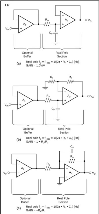
LP (Real-pole low-pass subcircuit). The basic low-pass subcircuit (LP) is shown in Figure 13A. A single pole is formed by RP and CP. A2 buffers the output to prevent
loading from subsequent stages. If high input impedance is needed, an optional buffer, A1, can be added to the input.
For an LP subcircuit with gain, use the optional circuit shown in Figure 13B.
For an LP subcircuit with inverting gain or attenuation, use the optional circuit shown in Figure 13C.
HP (Real-pole high-pass subcircuit). The basic high-pass subcircuit (HP) is shown in Figure 14A. A single pole is formed by RP and CP. A2 buffers the output to prevent
loading from subsequent stages. If high input impedance is needed, an optional buffer, A1, can be added to the input.
For an HP subcircuit with gain, use the optional circuit shown in Figure 14B.
For an HP subcircuit with inverting gain or attenuation, use the optional circuit shown in Figure 14C.
IF THE AUXILIARY OP AMP IN A UAF42 IS NOT USED
If the auxiliary op amp in a UAF42 is not used, connect it as a grounded unity-gain follower as shown in Figure 15. This will keep its inputs and output in the linear region of operation to prevent biasing anomalies which may affect the other op amps in the UAF42.
FIGURE 12. PP6 Inverting Pole-Pair/Zero Subcircuit.
ELIMINATING THE LP SUBCIRCUIT IN ODD-ORDER INVERSE CHEBYSHEV LOW-PASS FILTERS
Odd-order Inverse Chebyshev low-pass filters can be simpli-fied by eliminating the LP input section and forming the real pole in the first pole-pair/zero subcircuit. To form the real pole in the pole-pair/zero subcircuit, place a capacitor, C1, in
parallel with the summing amplifier feedback resistor, RZ3.
The real pole must be at the same frequency as in the LP subcircuit. One way to achieve this is to set C1 = CP and RZ3
= RP, where CP and RP are the values that were specified for
the LP section. Then, to keep the summing amplifier gains the same, multiply RZ1 and RZ2 by RP/RZ3.
Figures 16A and 16B show an example of the modification of a 3-pole circuit. It is a 347Hz-cutoff inverse Chebyshev low-pass filter. This example is from an application which required a low-pass filter with a notch for 400Hz system power-supply noise. Setting the cutoff at 347Hz produced the 400Hz notch. The standard filter (Figure 16A) consists of two subcircuits, an LP section followed by a PP4 section. In the simplified configuration (Figure 16B), the summing amplifier feedback resistor, RZ3 is changed from 10kΩ to
130kΩ and paralleled with a 0.01µF capacitor. Notice that these are the same values used for RP and CP in the LP
section of Figure 16A. To set correct the summing amplifier gain, resistors, RZ1 and RZ2 are multiplied by RP/RZ3 (130kΩ/
10kΩ). RZ1 and RZ2 must be greater than 2kΩ to prevent op
amp output overloading. If necessary, increase RZ1, RZ2, and
RZ3 by decreasing CP. PP6 A1 R2 50kΩ A2 A3 R4 50kΩ UAF42 11 R1 50kΩ RF1 RF2 C1 1000pF C2 1000pF 3 13 8 7 14 RQ R2A C1A C2A HP Out 1 12 A4 4 RZ1 5 Aux Out 6 RZ2 RZ3 LP Out RG VIN
FIGURE 15. Connect Unused Auxiliary Op Amps as FIGURE 13. Low-Pass (LP) Subcircuit: (a) Basic; (b) with
Noninverting Gain; (c) with Inverting Gain.
FIGURE 14. High-Pass (HP) Subcircuit: (a) Basic; (b) with Noninverting Gain; (c) with Inverting Gain.
A2 VO A1 VIN Optional Buffer Real Pole Section RP A2 VO A1 VIN Optional Buffer Real Pole Section A2 CP VO A1 VIN Optional Buffer Real Pole Section R2 R1 R1 CP RP CP RP (c) (b)
(a) Real pole fO = f–3dB = 1/(2π • RP • CP) [Hz] GAIN = 1.0V/V Real pole fO = f–3dB = 1/(2π • RP • CP) [Hz] GAIN = 1 + R2/R1 Real pole fO = f–3dB = 1/(2π • RP • CP) [Hz] GAIN = –RP/R1 (c) A2 VO CP A1 VIN Optional Buffer Real Pole Section R2 (b) A2 RP VO CP A1 VIN Optional Buffer Real Pole Section (a) A2 RP VO CP A1 VIN Optional Buffer Real Pole Section R2 R1 RP Real pole fO = f–3dB = 1/(2π • RP • CP) [Hz] GAIN = 1.0V/V Real pole fO = f–3dB = 1/(2π • RP • CP) [Hz] GAIN = 1 + R2/R1 Real pole fO = f–3dB = 1/(2π • RP • CP) [Hz] GAIN = –R2/RP UAF42 Fragment A4 4 6 5 LP HP
A1 R2 , 50k Ω A2 A3 50k Ω R4 50k Ω UAF42 11 R1 , 50k Ω RF1 1.37M Ω RF2 1.37M Ω C1 , 1000pF 2 13 8 7 14 3 1 A4 4 RZ1 , 9.53k Ω 5 Aux Out 6 RZ2 , 113k Ω RZ3 , 10k Ω RQ 549k Ω C2 , 1000pF A5 RP 130k Ω VIN CP 0.01µF
A1 R2 , 50k Ω A2 A3 50k Ω R4 50k Ω UAF42 11 R1 , 50k Ω RF1 1.37M Ω RF2 1.37M Ω C1 , 1000pF VIN 2 13 8 7 14 3 1 A4 4 124k Ω 5 Aux Out 6 RP , 130k Ω RQ 549k Ω 1.47M Ω CP , 0.01µF C2 , 1000pF
NOTE: To establish a real pole at the proper frequency and set the proper summing amplifier gain, the following changes were made to the pole-pair subcircuit: RZ3
changed to R
P
.
CP
added in parallel with R
Z3 . RZ1 and R Z2 multiplied by R P /R Z3 .
FIGURE 16B. Simplified Three-Pole 347Hz Inverse Chebyshev Low-Pass Filter (created by moving real pole to feedback of A
4
Q ENHANCEMENT
When the fO • Q product required for a pole-pair section is
above ≈100kHz at frequencies above ≈3kHz, op amp gain-bandwidth limitations can cause Q errors and gain peaking. To mitigate this effect, the program automatically compen-sates for the expected error by decreasing the design-Q according to a Q-compensation algorithm(1). When this
occurs, the value under the Q heading on the UAF42 Filter Component Values print-out will be marked with an asterisk indicating that it is the theoretical Q, not the actual design Q. The actual design Q will be shown under an added heading labeled QCOMP.
USING THE FilterPro™ PROGRAM
With each data entry, the program automatically calculates filter performance. This allows you to use a “what if” spreadsheet-type design approach. For example; you can quickly determine, by trial and error, how many poles are needed for a desired roll-off.
GETTING STARTED
The first time you use the program, you may want to follow these suggested steps.
Type FILTER42<ENTER> to start the program.
Use the arrow keys to move the cursor to the Filter Response section.
1) SELECT FILTER RESPONSE
Press <ENTER> to toggle through four response choices: Low-pass
High-pass Band-pass
Notch (band-reject)
When the desired response appears, move the cursor to the Filter Type section.
2) SELECT FILTER TYPE
Move the cursor to the desired filter type and press
<ENTER>. The selected filter type is highlighted and marked
with an asterisk. There are four filter-type choices: Butterworth Bessel
Chebyshev Inverse Chebyshev
If you choose Chebyshev, you must also enter ripple (i.e. pass-band ripple—see Chebyshev filter description). If you choose Inverse Chebyshev, you must also enter AMIN
(i.e. min attenuation or max gain in stop-band—see Inverse Chebyshev filter description).
3) ENTER FILTER ORDER
Move the cursor to the Filter Order line in the Parameters section. Enter filter order n (from 2 to 10).
4A) ENTER FILTER FREQUENCY
Move the cursor to the Filter Frequency line in the Param-eters section.
Low-pass/high-pass filter: enter the f–3dB or cutoff frequency.
Band-pass filter: enter the center frequency, fCENTER.
Band-reject (notch) filter: enter the notch frequency, fNOTCH.
If your filter is low-pass or high-pass, go to step 5.
4B) ENTER FILTER BANDWIDTH
If the filter is a band-pass or band-reject (notch), move the cursor to the bandwidth line and enter bandwidth.
If you press <ENTER> with no entry on the bandwidth line, you can enter fL and fH instead of bandwidth. fL and fH are
the f–3dB points with regard to the center frequency for
Butterworth and Bessel filters. They are the end of the ripple-band for Chebyshev types. This method of entry may force a change in center frequency or notch frequency.
5) PRINT-OUT COMPONENT VALUES
Press function key <F4> to print-out Filter Component Values and a Filter Block Diagram. Follow the instructions in the filter implementation section of this bulletin to as-semble a working filter.
USING THE PLOT FEATURE
A Plot feature allows you to view graphical results of filter gain and phase vs frequency. This feature is useful for comparing filter types.
To view a plot of the current filter design, press <F2>.
GRAPHIC DISPLAY COMMANDS
While viewing the graphic display, several commands can be used to compare filter responses:
<F1> or S—Saves the plot of the current design for future
recall.
<F2> or R—Recalls the Saved plot and plots it along with
the current design.
<F3> or Z—Plots a Zero dB reference line.
GRAPHIC DISPLAY CURSOR CONTROL
While viewing the graphics display you can also use the arrow keys to move a cursor and view gain and phase for plotted filter responses.
RESISTOR VALUES
With each data entry, the program automatically calculates resistor values. If external capacitors are needed, the pro-gram selects standard capacitor values and calculates exact resistor values for the filter you have selected. The 1% Resistors option in the Display menu can be used to calcu-late the closest standard 1% resistor values instead of exact resistor values. To use this feature, move the cursor to the resistors line in the Filter Response section and press (1) L.P. Huelsman and P. E. Allen, Theory and Design of Active
OP AMP SELECTION GUIDE (In Order of Increasing Slew Rate)
TA = 25°C, VS = ±15V, specifications typ, unless otherwise noted, min/max specifications are for high-grade model.
BW FPR (1) SR V
OS VOS/dT NOISE
OP AMP typ typ typ max max at 10kHz CCM (3)
MODEL (MHz) (kHz) (V/µs) (µV) (µV/°C) (nV/√Hz) (pF)
OPA177 0.6 3 0.2 10 ±0.1 8 1
OPA27 8 30 1.9 25 ±0.6 2.7 1
OPA2107 dual (2) 4.5 280 18 500 ±5 8 4
OPA602 (2) 6 500 35 250 ±2 12 3
OPA404 quad (2) 6 500 35 1000 ±3 typ 12 3
OPA627 (2) 16 875 55 100 ±0.8 4.5 7
UAF42 aux amp (2) 4 160 10 5000 ±3 typ 10 4
NOTES: (1) FPR is full power response at 20Vp-p as calculated from slew rate. (2) These op amps have FET inputs. (3) Common-mode input capacitance.
<ENTER>. The program will toggle between exact
resis-tors and standard 1% resisresis-tors.
CAPACITOR SELECTION
Even-order filters above 10Hz normally will not require external capacitors. Odd order filters require one external capacitor to set the real pole in the LP or HP section. Capacitor selection is very important for a high-performance filter. Capacitor behavior can vary significantly from ideal, introducing series resistance and inductance which limit Q. Also, nonlinearity of capacitance vs voltage causes distor-tion. The 1000pF capacitors in the UAF42 are high perfor-mance types laser trimmed to 0.5%.
If external capacitors are required, the recommended capaci-tor types are: NPO ceramic, silver mica, metallized polycar-bonate; and, for temperatures up to 85°C, polypropylene or polystyrene. Common ceramic capacitors with high dielec-tric constants, such as “high-K” types should be avoided— they can cause errors in filter circuits.
OP AMP SELECTION
Normally you can use the uncommitted fourth op amp in the UAF42 to implement any necessary LP, HP, or gain stages. If you must use additional op amps, it is important to choose an op amp that can provide the necessary DC precision, noise, distortion, and speed.
OP AMP SLEW RATE
The slew rate of the op amp must be greater than
π • VOPP • BANDWIDTH for adequate full-power response.
For example, operating at 100kHz with 20Vp-p output requires an op amp slew rate of at least 6.3V/µs. Burr-Brown offers an excellent selection of op amps which can be used for high performance active filter sections. The guide above lists some good choices.
OP AMP BANDWIDTH
As a rule of thumb, in low-pass and band-pass applications, op amp bandwidth should be at least 50 • GAIN • fO, where
GAIN = noise gain of the op amp configuration and fO = filter f–3dB or fCENTER frequency.
In high-pass and band-reject (notch) applications, the re-quired op amp bandwidth depends on the upper frequency of interest. As with most active filters, high-pass filters de-signed with the UAF42 turn into band-pass filters with an upper roll-off determined by the op amp bandwidth. Error due to op amp roll-off can be calculated as follows:
% = 100 1 – 1 (1 + f2 • (NGAIN)2/(UGBW)2)
(
)
or f = 200 – % • % • UGBW NGAIN • (% – 100) Where:% = Percent gain error f = Frequency of interest (Hz) NGAIN = Noise gain of op amp (V/V)
= GAIN of noninverting configuration = 1 + |GAIN| of inverting configuration UGBW = Unity-gain bandwidth of the op amp (Hz):
GAIN ACCURACY (%) f (NGAIN)/(UGBW)
–29.29 1.000 –10.00 0.484 –1.00 0.142 –0.10 0.045 –0.01 0.014 EXAMPLES OF MEASURED UAF42 FILTER RESPONSE
Figures 17 and 18 show actual measured magnitude re-sponse plots for 5th-order 5kHz Butterworth, 3dB Chebyshev, –60dB Inverse Chebyshev and Bessel low-pass filters de-signed with the program and implemented with UAF42s. As can be seen, the initial roll-off of the Chebyshev filter is the fastest and the roll-off of the Bessel filter is the slowest. However, each of the 5th-order all-pole filters ultimately rolls off at –N • 20dB/decade, where N is the filter order (–100dB/decade for a 5-pole filter).
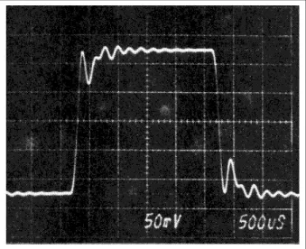
The oscilloscope photographs (Figures 19-22) show the step response for each filter. As expected, the Chebyshev filter has the most ringing, while the Bessel has the least.
FIGURE 17. Gain vs Frequency for Fifth-Order 5kHz (a) Butterworth, (b) 3dB Chebyshev, (c) –60dB Inverse Chebyshev, and (d) Bessel Unity-Gain Low-Pass Filters, Showing Overall Fil-ter Response. Frequency (Hz) 50 100 1k 50k Gain (dB) 10 0 –10 –20 –30 –40 –50 –60 –70 –80 –90 10k (a) (d) (b) (c)
FIGURE 18. Gain vs Frequency for Fifth-Order 5kHz (a) Butterworth, (b) 3dB Chebyshev, (c) –60dB Inverse Chebyshev, and (d) Bessel Unity-Gain Low-Pass Filters, Showing Transition-Band Detail. Frequency (Hz) 100 1k 10k Gain (dB) 3 0 –3 –6 –9 –12 –15 –18 –21 –24 –27 (a) (d) (b) (c)
FIGURE 19. Step Response of Fifth-Order 5kHz Butterworth Low-Pass Filter.
FIGURE 21. Step Response of Fifth-Order 5kHz, –60dB Inverse Chebyshev Low-Pass Filter.
FIGURE 20. Step Response of Fifth-Order 5kHz, 3dB Ripple Chebyshev Low-Pass Filter.
FIGURE 22. Step Response of Fifth-Order 5kHz Bessel Low-Pass Filter.
IMPORTANT NOTICE
Texas Instruments and its subsidiaries (TI) reserve the right to make changes to their products or to discontinue any product or service without notice, and advise customers to obtain the latest version of relevant information to verify, before placing orders, that information being relied on is current and complete. All products are sold subject to the terms and conditions of sale supplied at the time of order acknowledgment, including those pertaining to warranty, patent infringement, and limitation of liability.
TI warrants performance of its semiconductor products to the specifications applicable at the time of sale in accordance with TI’s standard warranty. Testing and other quality control techniques are utilized to the extent TI deems necessary to support this warranty. Specific testing of all parameters of each device is not necessarily performed, except those mandated by government requirements.
Customers are responsible for their applications using TI components.
In order to minimize risks associated with the customer’s applications, adequate design and operating safeguards must be provided by the customer to minimize inherent or procedural hazards.
TI assumes no liability for applications assistance or customer product design. TI does not warrant or represent that any license, either express or implied, is granted under any patent right, copyright, mask work right, or other intellectual property right of TI covering or relating to any combination, machine, or process in which such semiconductor products or services might be or are used. TI’s publication of information regarding any third party’s products or services does not constitute TI’s approval, warranty or endorsement thereof.

![Bis{5 methyl 2 phenyl 4 [(3 tolylamino κN)phenylmethylene] 1H pyrazol 3(4H) onato κO}cobalt(II)](data:image/gif;base64,R0lGODlhAQABAIAAAP///wAAACH5BAEAAAAALAAAAAABAAEAAAICRAEAOw==)