An Optimal Control Scheme for a Class of
Duty-Cycle Modulation Buck Choppers:
Analog Design and Virtual Simulation
Paul Owoundi Etouke
1, Léandre Nneme Nneme
2, Jean Mbihi
3 1, 2, 3Research
Laboratory of Computer Science Engineering and AutomationENSET, University of Douala Douala, Cameroun
Email :
1 [email protected], [email protected],
3 [email protected]Abstract – This paper presents a design methodology and a virtual simulation framework, of the optimal feedback control scheme for DCM (duty-cycle modulation) Buck choppers. The transfer function of an open loop DCM chopper, is built from the numerical analysis of a virtual step response, with Ref = 2 volts as step control input. Then, the optimal PID controller for DCM Buck Choppers is formulated and synthetized as a LQR (Linear Quadratic Regulator) equivalent control, and the associated Riccati equations is easily solvable using Matlab/LQR tool. As a relevant implication, the parameters of the corresponding optimal PID, are straightforwardly obtained from the LQR gains according to a LQR/PID equivalence principle, which is proven for a relevant class of second order dynamic systems. In addition, in order to show the feasibility of the designed optimal PID control scheme, a whole prototyping DCM Buck chopper with given operating conditions ( main DC supplied (12 V), load resistance (3.3 Ω), basic DCM frequency (30 kHz)), is virtually implemented and well tested using Multisim. The virtual simulation results obtained from numerous operating conditions (e.g., open loop, closed loop, load variations), are presented and discussed. Furthermore, relevant results and findings are reported, e.g., transient characteristics (i.e. controllability, stability, overshoot (4%), and time response (1.5 ms) and static performance levels (e.g. static error (0 %), high robustness under 50 % load variations). These results are a great challenge for the first virtual DCM Buck chopper, operating under a well-tested optimal PID-based control policy.
Keywords - DCM Buck choppers; optimal PID controller; linear quadratic regulator; LQR/PID equivalence principle; analog design, Virtual simulation.
I. INTRODUCTION
The modern DCM (Duty-Cycle Modulation), developed and published since 2004 [1], has increasingly become a versatile modulation technique, offering minimum realization cost and optimal quality, in a wide variety of signal processing systems. A complete literature review about the DCM
technique and its potential applications, are provided in a recent Review paper [2]. Indeed, the main relevant applications of DCM principles and related prototyping realization are: Analog-to-digital conversion [3-7], digital-to-analog conversion [7-12], electronic signal transmission [2, 13-14], and driving design for power electronics [6, 15-18].
As a scientific context, this paper falls into to the class of research works related to optimal control of power converters, with a Buck chopper architecture, equipped with low cost and high quality driver. However, it is worth nothing that a few optimal PID-based and LQR-based control schemes are encountered in the literature [19.22]. In addition the feasibility of DCM Buck choppers equipped with a standard PID controller, has been proven already in a pioneering work presented in [18]. However, according to our best knowledge, the optimization feedback control problem of DCM Buck converters, has not been formulated and solved in the literature.
Therefore, the scientific contribution of this paper, is to present a new design methodology and a well-tested virtual realization, of an optimal feedback control scheme for DCM Buck choppers. The relevant contribution of this paper has been to successfully design and implement a well-tested prototyping optimal PID-based control scheme, from a proven LQR/PID equivalence principle, for the sake of minimum virtual electronic realization, within Multisim Framework.
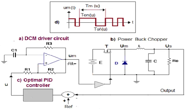
Figure 1. PID control scheme for DCM Buck choppers [18].
II. DESIGN METHODOLOGY OF THE OPTIMAL CONTROLLER FOR DCM BUCK CHOPPERS
A. Recall on PID control for DCM Buck Choppers
The PID control scheme for DCM Buck Choppers is shown in Fig.1. It consists of many main parts including a DCM circuit (Fig. 1a), a power Buck Chopper (Fig. 1b) where the notation E, L-C, Ro, Us, u and um, stands for main DC source, power filter, load resistance and output voltage, control and DCM wave respectively); and a standard PID controller (Fig. 1c). It is obvious that the DCM circuit shown in Fig. 1a, offers exceptional visual qualities, including a single state hardware architecture, an embedded clock, and both positive and negative feedback loops for the sake of better operating robustness under infected modulating waves.
The general shape of the DCM wave shown in Fig. 1d, is a switching aperiodic wave, where over a DCM period Tm(u) = Ton(u) + Tof(u), the notations Ton(u) and Tof(u) stand for ON pulse width and OF pulse width respectively. Given α1 = R1/(R1+R2), and α2 = 1- α1, then the duty-cycle Rm(u) of the DCM signal um as proven and reported in the literature [1, 9], is given by equation (1), given (2).
2 1 2 1 2 2 2 1 2 2 2 1 ( ) ( )(1
)
ln
(
1)
1
( )
2
(1
)
ln
(
1)
m m on u m uu
E
u
E
T
R u
p u
T
u
E
u
E
(1) where, 1 2 2 1 1 1(1
)
1
log
1
mE
p
(2)The validity of the linear approximation used in (1), will be justified later in section 3, from numerical analysis fundamentals. In addition, it has been shown also in the literature [1, 9], that the DCM frequency fm(u) and its maximum fm(0) are given by (4)
2 2 2 1 2 2 2 1 3 11
( )
,
(1
)
(
1)
mf
x
x
E
R C Log
x
E
(3) 1 1 3 11
(0)
1
2
1
mf
R C Log
(4)Unlike the well known PWM (Pulse Width Modulation) technique, for which the modulating signal is encapsulated in Ton(u) under a constant Tm(u), the DCM period Tm(u) and pulse width Ton(u) simultaneous vary, the modulating signal being encapsulated into Rm(u). In this paper, we resort to the same power DCM Buck Chopper used in [18], with open loop transfer function given by,
2
2 2
( )
( )
( )
2
s n
n n
K
Y s
G s
U s
s
s
(5)where Y(s) = Uo(s), and Ks,
n2 and ξ could be obtained according to relationships (6-8) from those of the step response of a virtual realization, i.e., Ref (step control input), Y(∞), D (overshoot), Tr (setting time), and r (% of setting time).
0 S s Y K E (Static gain) (6)
2 2
))
(log(
)
log(
D
D
(Damping coefficient) (7)
Tr
r
n
)
100
log(
(Natural frequency (8)Figure 2. PID control scheme for DCM Buck choppers
B. DESIGN OF OPTIMAL PID CONTROLLER
A PID control scheme for DCM Buck choppers, with transfer function (5), is presented in figure 2. After straightforward algebraic developments from Fig. 2, the closed loop transfer function of the resulting PID control system, is given by (9).
It is clear that formulating and solving an optimal control problem from (8), in order to find optimal PID gains Kp, Ki and Kd, is both an intractable and tedious work. Fortunately, this optimization control problem could be easily formulated and solved from a suitable state space representation, as it is proven next.
The optimal feedback control for DCM Buck choppers, is formulated as an optimal LQR control problem for a suitable choice of state variables x1, x2 and x3 as outlined in Fig. 2.
In a time domain, let consider the 2nd order ODE (ordinary differential equation) described by (10), associated with the transfer function (5), and the choice of state variable x1, x2 and x3 given by (11), as located in Fig. 2.
2
2 2
( )
2
n n s n( )
d y t
dy
y
K
u t
dt
dt
(10)1
Re
,
2,
3de
x
e
f
y x
e dt
x
dt
(11)For a constant set voltage denoted Ref, the ODE (10) given (11) leads to (12), which can be organized into matrix form (13) or (14) equivalently.
1 3 2 1 2 2 3 1 3
(Re
)
2
n( )
n s n
dx
de
dy
x
dt
dt
dt
dx
e
x
dt
dx
f
x
x
K
u t
dt
(12)2 2 2
0 0 1 0 0
( )
1 0 0 ( ) 0 ( ) 0 Ref
0 2
( ) [ -1 0 0 ] ( ) Ref
n
n s n n
dx t
x t u t
dt
K
y t x t
(13)
2 2 2
0 0 1
( ) ( )
1 0 0 ( )
Re 0 2
( ) ( ) [ -1 0 0 ] ( ) [ 0 1 ]
Re 0 0 0 0 n
n s n n
u t dx t x t f dt K u t
y t x t
f (14)
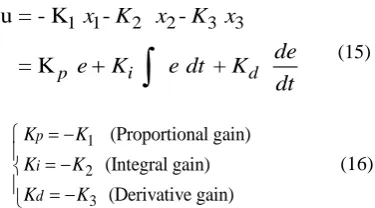
As a fundamental result, any arbitrary state feedback control u(t), applied to (14), is given by (15), from which it becomes obvious that, (15) is a pure PID control policy, with gains given by (16).
1 1 2 2 3 3
u = - K -
-
= K
p i+
dx
K
x
K x
de
e
K
e dt
K
dt
(15)1 2 3 (Proportional gain) (Integral gain) (Derivative gain) p i d K K K K K K (16)
Therefore, for the same dynamic system (5), an optimal PID controller and the LQR with optimization criterion (17), have equivalent feedback control gains.
0
(
T( )
cx(t)
T( )
cu(t))
J
x t Q
u
t R
dt
(17)2 2
3 2 2 2 2
p
p i
i
(9)
(
s +K s +K )
( )
( )
Re ( )
(2
)
(1
)
K
d
s n
d
n s n n s s n
K
K
Y s
F s
f s
s
K K
s
K K s
K
Figure 3. Multisim schematic diagram of a DCM Buck chopper under optimal PID control.
Subsequently, the optimal gain vector K = [K1 = Kp K2 = Ki K3 = Kd] can be obtained by solving the Riccati Equation (18) [23-24]:
Q
A K
cTKA
cKB R B K
c 1 cT0
(18)
Fortunately, solving (18) in a practical context, is easy using Matlab/LQR command. As a result, the optimal LQR state feedback, which is equivalent to an optimal PID control is given by (19).
2 2 2 2
1 2
2 2
s s s
s
0 0 1
( )
1 0 0 ( )
- K K 2 3 K
0 0 Ref
K
( ) [ -1 0 0 ] ( ) Ref -
n
n n n n
n n
dx t
x t dt
K K K
y t x t
(19)
B. PROTOTYPING SYSTEM
The prototyping DCM Buck chopper studied in this section has been implemented in Multisim platform. Its electronic schematic diagram presented in Fig. 3. The analog PID control part consists of a few simple operational amplifier circuits, numbered as follows: 1 (difference circuit with output e = Ref – Uo; 2 (PID input circuit); and 3 (Output inverter). Additional relevant parts are numbered also: 4 (DCM driver circuit); 5 (Power Buck chopper; 6 (Main power supply), 7 (Virtual multichannel oscilloscope); and 5 (Load variation unit). Following circuit analysis techniques, it is easy to show that the transfer function of the PID controller is given by (20),
( ) = ( )
b a
a b
R C
Upid s
E s R C +
1
a b R C
1
s+R Cb a s (20) then, the parameters of the optimal PID controller are given in terms of those of electronic building components, as follows:
p b a, i 1 , d b a
a b a b
R C
K K K R C
R C R C
Part Name Symbols Valeurs
Power Buck chopper
Main Power supply E 12 V
Control power suply ± Vcc ±12 V
Resistive loads Ro, Ro1 3.3Ω
Power MOSFET Q IRLZ14
Diode D HFAD04TB60
Difference circuit
Resistance R4 100 kΩ
Resistance R5 100 kΩ
Resistance R6 100 kΩ
Resistance R7 100 kΩ
Optimal PID/LQR
State matrix cost Diag(q1, q2, q3) q1=80; q2=1e04; q3=1e-3
Control cost r 0.4
Proportional gain Kp 14.3316
Integral gain Ki 158.114
Derivative gain Kd 0.0499
Optimal PID circuit
Operational amplifiers U1j, j = 1, 2, 3, 4 TL082CD
Resistance Ra 120 kΩ
Capacitance Ca 0.725 uF
Resistance Rb 1.65 MΩ
Capacitance Cb 0.53 nF
DCM circuit
Resistance R1 1.2 kΩ
Resistance R2 10 kΩ
Resistance R3 2.32 kΩ
Capacitance C1 33 nF
Resistance R10 1 kΩ
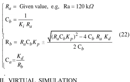
Indeed, the numerical values of parameters Ra, Ca, Rb and Cb, can be computed according to a simple algorithm (22).
2
Given value, e.g, Ra = 120 k
1 C
( C ) C
R C ±
2 C 4
C = a
b i a
a b p b a d
b a b p
b
d a
b R
K R
R K R K
R K
K R
(22)
. III. VIRTUAL SIMULATION
A. TECHNICAL INFORMATION AND DATA
The technical information and data used for the prototyping optimal PID-based control system, are summarized in Table 1 provided above. Using the open loop step response (Ref = 2 volts step input) of the virtual prototyping DCM Buck chopper (see Fig. 4), the set of parameters {Ks = 2.7494, ωn = 2116.7 rad/s, ξ = 0.3626} of the transfer function (23) have been identified according to (6), (7) and (8). It is worth noting the main characteristics of the open loop control are: overshoot (17 %), time response (3.66 ms), and static error (64%).
2
2 2
2
( )
( )
( )
2
(4480400)
2.7494
1535
4480400
s nn n
K
Y s
G s
U s
s
s
s
s
(23)
Figure 4. Open loop step response in Matlab
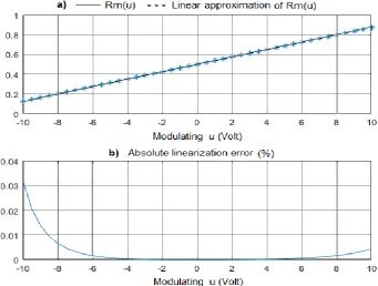
Figure 5. Rm(u) and its linear approximation
Figure 6. Virtual simulation of the open loop control systems for Ref = 2 volts
Furthermore, as predicted earlier in (3), Fig. 5 shows a piecewise perfect closeness between the exact nonlinear duty-cycle Rm(u) and its linear approximation. It is a challenge to discover from Fig. 5 that the absolute error incurred when using the linear approximation of the duty-cycle function Rm(u), is less than 3% within the modulating range [-10 [-10], while it becomes piecewise zero when the
modulating control falls into the range of [-4 4] volts. As a relevant conclusion, the feasibility of the prototyping DCM Buck chopper is outlined.
B. VISUAL SIMULATION ANS RESULTS
Figure 7. Step response of the nominal optimal control system (Ref = 6 volts)
Figure 8. Robustness under a permanent disturbance (50 % load variation)
Fig. 7 presents the visual waveforms of DCM signal um and output voltage Uo delivered to the nominal load Rs = 3.3 Ω. In this case, the optimal characteristics provided are as follows: Overshoot (D = 4 %), time response (Tr = 1.5 ms), static error (0 V). These characteristics are a challenge compared to those of the open loop control. Fig. 8 shows the behavior of the optimal feedback control system, under a permanent disturbance (50 % load variation), applied in steady operating state from time = 3.28 ms. It is worth noting that, the undesired deviation of the output Uo due to the permanent disturbance, is cancelled before 1.23 ms time interval. These performance levels and associated findings, are a great challenge for the first virtual prototyping DCM Buck chopper, operating under optimal PID-based control policy.
IV. CONCLUSION
AUTHORS CONTRIBUTIONS
Paul Owoundi Etouke contributed to the dynamic modelling of buck choppers, and to the development of the well tested virtual workbench, used to produces relevant results presented in the paper.
Leandre Nneme Nneme contributed to the synthesis of the LQR, from which the equivalent optimal PID controller has been synthetized. He also reinforced the results by the robustness analysis.
Jean Mbihi contributed to the edition of the abstract, as well as the introduction and conclusion of the paper. He also contributed to the technical specification of the prototyping buck chopper to be simulated.
REFERENCES
[1] J. Mbihi. F. Ndjali Beng, M. Kom, and L. Nneme Nneme, „‟A Novel Analog-to-Digital Conversion technique using Nonlinear Duty-Cycle Modulation‟‟, International Journal of Electronics and Computer Science Engineering. Volume1, Number 3, pp. 818-825.2012,
www.ijecse.org.
[2] L. Nneme Nneme, B. L. Moffo, G. B. Sonfack and J. Mbihi, "A Review of Multipurpose Duty-cycle Modulation Technology in Electrical engineering and Industrial Electronics", Journal of Electrical Engineering, Electronics, Control and Computer Science ", Vol. 4, Issue 12, pp. 9-18, 2018
[3] J. Mbihi, F. Ndjali Beng, M. Kom, L. Nneme Nneme, "A Novel Analog-to-digital conversion Technique using nonlinear duty-cycle modulation", International Journal of Electronics and Computer Science Engineering, Volume 1, Number 3, pp 818-825, 2012, India.
[4] J. Mbihi and L. Nneme Nneme, "A Multi-Channel Analog-To-Digital Conversion Technique Using Parallel Duty-Cycle Modulation", International Journal of Electronics and Computer Science Engineering, Volume 1, Number 3, pp 826-833, 2012,India, ISSN: 2277- 1956, www.ijecse.org. [5] G. Sonfack, J. Mbihi and B. Lonla Moffo, “Optimal
Duty-Cycle Modulation Scheme for Analog-To-Digital Conversion Systems”, International Journal of Electrical, Computer, Energetic, Electronic and Communication Engineering”, © World Academy of Science, Engineering and Technology. March 2017, vol. 123(3). 348 – 354, March 2017
[6] G. B. Sonfack, J. Mbihi, “ FPGA-Based Analog-to-Digital Conversion via Optimal Duty-Cycle Modulation”, Journal of Electrical and Electronic Engineering, 8(2), pp. 29-36, 2018. [7] J. Mbihi , "Dynamic Modelling and Virtual Simulation of Digital Duty-Cycle Modulation Control Drivers",
International Journal of Electrical, Computer, Energetic, Electronic and Communication Engineering , Vol 11, No 4, pp. 472-477, 2017, © WASET (World Academic of Science, engineering and Technology), USA.
[8] J. Mbihi et A. Motto, "Informatique industrielle - Instrumentation virtuelle assistée par ordinateur: Principes et techniques, Cours et exercices corrigés", 240 pages, Editions Ellipses, collection TechnoSup, 23 Octobre 2012, France,
www.editions-ellipses.fr
[9] B. Lonla Moffo, J. Mbihi , "A Novel Digital Duty-Cycle Modulation Scheme for FPGA-Based Digital-to-Analog Conversion", © IEEE Transactions on Circuits and Systems II , Vo. 62, N°6, pp. 543-547, June 2015.
[10] B. L. Moffo, J. Mbihi , L. Nneme. Nneme, “FPGA-Based Multichannel Digital Duty-Cycle Modulation and Application to Simultaneous Generation of Analog Signals ”, Journal of Electronic Design Technology, Volume 8, Issue 1, pp. 23-35, Août (August) 2017, India, www.stmjournals.com. [11] B. Lonla Moffo, J. Mbihi, L. Nneme Nneme and Martin
KOM, "A novel digital-to-analog conversion technique using duty-cycle modulation”, International Journal of Circuits, Systems and Signal processing, Issue 1, Vol. 7, pp 42-49, May 2013, Bulgaria, © www.naun.org/main/NAUN/ [12] J. Mbihi, F. Ndjali Beng, M. Kom, L. Nneme Nneme, "A
Novel Analog-to-digital conversion Technique using nonlinear duty-cycle modulation", International Journal of Electronics and Computer Science Engineering, Volume 1, Number 3, pp 818-825, 2012, India.
[13] L. Nneme Nneme, J. Mbihi, "Modeling and Simulation of a New Duty-Cycle Modulation Scheme for Signal Transmission System", American Journal of Electrical and Electronic Engineering (AJEEE), Vol 2, N° 3, pp. 82-87,
2014, USA , DOI:10.12691/ajeee-2-3-4.
[14] B. Lonla Moffo, J.Mbihi, Leandre Nneme Nneme, "A low cost and high quality duty-cycle modulation scheme and applications", International Journal of Electrical, Computer, Energetic, Electronic and communication Engineering, Vol 8, N° 3, pp. 82-88, 2014, © WASET (World Academic of Science, engineering and Technology), USA.
[15] A. Obono Biyobo, L. Nneme Nneme and J. Mbihi, "A Novel Sine Duty-Cycle Modulation Control Scheme for Photovoltaic Single-Phase Power Inverters", WSEAS Transactions on Circuits and Systems, pp. 105-113, 2018. [16] Y. P. Dangwe Sounsoumo, Jean Mbihi, Haman-djalo and
Joseph Yves Effa, "Virtual Digital Control Scheme for a Duty-Cycle Modulation Boost Converter ", Journal of Computer Science and Control Systems, Volume 10, No 2, pp. 22-27, October 2017, Romania.
[17] Y. P. Dangwe Sounsoumou, Haman DJALO , Jean Mbihiet J. Y. EFFA , " Modélisation et simulation virtuelle d‟un nouveau schéma de réglage de hacheurs Boost à commande rapprochée par modulation en rapport cyclique ", Journal Afrique Science , pp. 176-185, Vol. 13, No. 1, 2017, Côte d'Ivoire, http://www.afriquescience.info.
[18] J. Mbihi, L. Nneme Nneme, "A novel Control Scheme for Buck Power Converters using Duty-Cycle Modulation",
International Journal of Power Electronics, Vol. 5, N°3/4, pp
185 - 199, October 2013, Switzerlan..
[19] A. Mohammadbagheri 1, Narges Zaeri and M. Yaghoobi, “Comparison Performance Between PID and LQR Controllers for 4-leg Voltage-Source Inverters”, pp. 220-234,
2011 International Conference on Circuits, System and Simulation, IPCSIT vol.7 (2011) © IACSIT Press, Singapore
[20] R. dwivedi1, D. Dohare2, “PID Conventional Controller and LQR Optimal controller for Speed analysis of DC Motor: A Comparative Study”, International Research Journal of Engineering and Technology, Volume: 02 Issue: 08, pp. 508-515, | Nov-2015, www.irjet.net.
[21] V. Kumar, J. Jeromeb, “LQR based optimal tuning of PID controller for trajectory tracking of Magnetic Levitation” Procedia Engineering 64 ( 2013 ) 254 – 264, System, International Conference On DESIGN AND MANUFACTURING, IConDM 2013.
[22] R. T. O‟Brien, “Optimal PID Controller Design using Standard Optimal Control Techniques”, 2008 American Control Conference Westin Seattle Hotel, Seattle, Washington, USA, June 11-13, 2008.
[23] J. Mbihi, "Techniques Avancées et Technologie de Commande et Régulation Assistée par Ordinateur", © ISTE Editions , 248 pages, Janvier 2018, Londres, Angleterre. ISBN : 978-1-78405-325-3 (papier), ISBN : 978-1-78406-325-2 (ebook), www.iste.co.uk.
![[N,N′ Bis(3 methoxy 2 oxidobenzylidene)ethane 1,2 diaminium κ4O,O′,O′′,O′′′]tris(nitrato κ2O,O′)erbium(III)](data:image/gif;base64,R0lGODlhAQABAIAAAP///wAAACH5BAEAAAAALAAAAAABAAEAAAICRAEAOw==)