Journal of Electrical Engineering,
Electronics, Control and Computer Science
JEEECCS, Volume 1, Issue 2, pages 9-14, 2015
Implementation of Active Loads MOSFET
Amplifiers in Vocational Training
Ionel BOSTAN
Department of Electronics and Computers Science University of Piteşti
Piteşti, Romania [email protected]
Authors Name/s per 2nd Affiliation (Author)
line 1 (of Affiliation): dept. name of organization line 2: name of organization, acronyms acceptable
line 3: City, Country line 4: e-mail address if desired
Abstract – In this paper is presented one electronic board with highly educational role, designed by author, which can be used in vocational training in the field of analog electronic. This board provides all necessary resources in order to study the advantages and disadvantages of NMOS common-sources amplifiers with or without active loads. Also this board can be useful in other experiment such MOSFET parameters estimation, studying current PMOS current mirrors, etc.
Keywords - educational electronic board, passive load common-source amplifier, active load common-source amplifier, current mirrors, analog electronics, MOSFET transistor, vocational training.
I. INTRODUCTION
For a long period of time vocational education and training (VET) played only a minor role in European countries because general opinion was that it offered less good jobs and even less promotion opportunities. In order to make VET more attractive, a series of European instruments was developed since Copenhagen Declaration, such as: (1) European Qualifications Framework (EQF); (2) European Credit system for Vocational Education and Training (ECVET); (3) European Qualifications Framework (EQF); (4) Europass framework. All these instruments provide a legal framework to support cooperation in quality assurance; recognition of qualifications; mobility and lifelong learning. The growing importance of VET it is recognized in various documents elaborated by European Centre for the Development of Vocational Training, [1].
To improve the quality, efficiency and attractiveness of VET, European Union establishes eleven strategic objectives for 2011-2020 in Bruges Communiqué. Among them, from my point of view, “encourage practical activities and the provision of high-quality information and guidance” [2], will have a great long-term impact.
In any field of vocational education, in order to make relevant practical activities, appropriate teaching materials are mandatory. In this direction, EU offer constant financial support for developing new educational materials and methodologies via transnational projects. A good example of cooperation of different educational entity in developing educational materials that meet the requirements of
European community is One2One [3]. Even so, the effort to develop new educational equipment must be a constant concern of each teacher [4].
In author opinion, for Analog Integrated Circuit subject there is a relative lack of appropriate educational boards due to the following facts: (1) all circuits must operate at very low bias currents; (2) each gain stage usually operates on active internal loads; (3) great difficulties in ensuring appropriate biasing of each gain stage; (4) multistage amplifier requires direct coupling.
The most common building blocks in analog integrated circuits are voltage amplifiers. Among them, voltage amplifiers using active loads are used in almost every analog integrated circuit due to their superior performance over standard configurations with passive loads. The main tow benefits of active load configurations are: (1) much higher gain at the much lower bias current; (2) active load is much easier to fabricate then high value resistor. On the other hand, due to the high gain, active load configurations are more difficult to bias, therefore requires additional circuits in order to ensure correct operation.
From didactical point of view, taking into account the importance of the active load configurations in microelectronics, it is very important for students to have the opportunity to make practical lab experiments, not only SPICE simulations, in order to have a better understanding of these circuits.
In this paper is presented one electronic board with highly educational role, which can be useful in vocational training in the field of analog electronics. With this board students can make practical experiments in order to understand the advantage and disadvantage of common-source (CS) amplifiers with or without active loads.
II. TYPICAL CSAMPLIFIERS TOPOLOGIES
The most common loads used for common-source amplifier are:
passive (resistive) load;
current-source load;
composite load made of MOSFET diode connected in parallel with current-source.
First type of load is used for discrete implementation and the last three are used only inside of integrate circuits. In this section are presented the main characteristics for each type of load for CS amplifier
A. Common-Source Amplifier with Passive Load The first topology of amplifier which can be study on educational board is common-source stage with passive load connected as in Figure 1.
Figure 1. Common-source amplifier with passive load
For passive load CS stage, the voltage gain is estimated with relation (1)
a
v g
mR
L g
m(r
dsR
D)
OV D ox
n D GS
D
m VI I C WL IV
g
5 0 2
.
where:
gm represent the transconductance of active element M1;
VOVrepresent the overdrive voltage of active element M1 at bias current ID;
In many practical situations for this type of amplifier, condition rdsRD is met and therefore voltage gain can be approximately calculated with relation (3)
v m D D n ox RD
L W C I R
g
a
2
For passive load CS configuration, the maximum voltage gain is obtained for no load operation [5], [6], [7], is named intrinsic gain and is given by relation (4)
OV DD max
v VV
a
5
0.
From last tow relations it can be seen that maximal voltage gain is limited by power supply voltage VDD, and bias current ID.
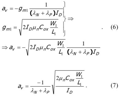
B. Common-Source Amplifier with Current-Source Load
The second topology which can be study on educational board is CS with active load connected as in Figure 2.
Figure 2. Common-source amplifier with active load (current source generator implemented with M2)
For this configuration, the voltage gain is calculated using relations (5):
D P ds
D N ds
ds ds
ds ds ds
ds L
ds ds m L
m v
I
r
I
r
r
r
r
r
r
r
R
r
r
g
R
g
a
1 1
2 1
2 1
2 1 2
1
2 1 1
1 ( )
D P N m
v g I
a
) (
1 1
Furthermore, taking into the account the expressions of transconductance, voltage gain can be rewrite as:
D P N ox
n D v
ox n D m
D P N m v
I L
W C I a
L W C I g
I g
a
) (
) (
1 2
2
1
1 1 1
1 1
1
D ox n
P N
v I L
W C
a 1
1 2
1
1 1 05 5 0 1 1 OV Aeq OV P N v V V V a . .
From last relation it can be seen one main advantage of this topology: voltage gain does not longer depend on supply voltage VDD, therefore it can be used for low voltage supply.
C. Common-Source Amplifier with Diode – Connected PMOS Load
The third topology implemented on educational board is CS stage with diode-connected PMOS load as shown in Figure 3. This topology it is characterized by a very good linearity and has a large bandwidth.
Figure 3. CS stage with diode-connected PMOS load
The drawback of this topology is given by low voltage gain [5], [6], [7].
2 1 2 1 2 1 1 1 1 1 m m v m ds m ds m L m v
g
g
a
g
r
g
r
g
R
g
a
Voltage gain relation (9) can be rewritten as:
2 2 2 1 1 1 2 2 2 1 1 1 2 2 2 2 1 1 1 1 2 1 2 2 2 2 L W C I L W C I L W C I L W C I a L W C I g L W C I g g g a ox p D ox n D ox p D ox n D v ox p D m ox n D m m m v
and taking into account that ID1=ID2=ID, it can obtain:
2 2 1 1
L
W
C
L
W
C
a
ox p ox n v
Another advantage of this topology can be deducted from last relation: voltage gain can be set by tuning the physical dimension of the transistors and it is independent of voltage supply and bias current.
D. Common-Source Amplifier with Diode – Connected PMOS Load
The last topology implemented on educational board is common-source with combined load in order to improve the voltage gain. For this topology the load has two elements: one PMOS diode (M2) connected in parallel with a current source, as is presented in Fig 4.
Figure 4. CS amplifier with combined load
In order to get the voltage gain for combined load CS stage it can be started with relation (10) and replace the currents ID1 and ID2 with valued imposed by electric diagram from Fig 4.
2 2 2 1 1 2 2 2 2 1 1 1 L W C I L W C I I L W C I L W C I a ox p ox n B ox p D ox n D v ( ) 2 2 1 1 2 2
L
W
C
L
W
C
I
I
I
a
ox p ox n B v
v B
a
v PMOS LOADI
I
I
a
_ _2
2
III. EUCATIONAL BOARD PRESENTATION
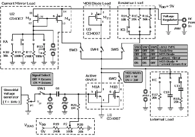
The educational board presented in this section was equipped with all necessary resources in order to study all typical common-source topologies presented in previous section.
All MOSFET transistors used in this board are taken from low cost integrated circuits type CD4007 or similar [8].
The main functional blocks of educational board can be seen in Figure 5: active element; internal load; external load (signal load); input signal generator and biasing circuit for active element.
The active element used in all CS stage topologies is M1A which is taken from one CD4007 integrated circuit. For educational purposed, the channel width of active element can be doubled by closing the switch SW2.
Different type of internal load can be selected using different combinations on switches SW3, SW4 and SW4. For instance, in case of current source load, switch SW3 must be ON and the other two must be OFF. Internal current generator load is implemented with current mirror, M3&M4, which allows us to modify the value of the reference current, via selector KA.
In a similar way, passive internal load can be selected with SW5 in position ON and value of the load can be chose with selector KC. External type of load can be selected using KD. Using potentiometer P2 we can bias the active element, according with the value of ID.
Taking into account the educational role, the board has four measuring points in order to get access to
measure different voltages or in order to use oscilloscope to display input/output signals.
This board can be used in a series of lab experiments such as:
determination of MOSFET quadratic model parameters [9];
studying the effect of physical dimension of the transistor over the voltage gain and over the overdrive voltage;
studying PMOS current mirrors;
studying common-source NMOS amplifier with different types of internal loads: resistive load, current source load, PMOS diode load, combined load (PMOS diode connected in parallel with current source);
studying the effect of the different types of external load over the voltage gain and over the output signal waveform;
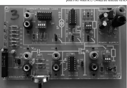
Considering all above facilities of this board which can be seen in Figure 6, I hope it will be a very useful tool in lab experiments for vocational training.
IV. EDUCATIONAL EXPERIMENTS SETUP
All transistors used in educational board are taken from low cost CD4007 integrated circuits which are mainly designed for use in logic circuits; therefore no data are available regarding the main parameters of the transistors. Even worse is that we can find big difference between circuits made by various manufacturers. From these reasons, the first experiments with this board must be targeted to more accurate determination of the main parameters of the MOSFET transistors.
In order to determinate the numerical values of the main parameters for NMOS transistor two measurements are needed over the gate-source voltage (VGS), at two different value of drain current ID. First VGS determination (denoted VGS1) is made at a current drain ID1=100A and the second determination (denoted VGS2) is made at a current drain ID2 = 4ID1 = 400A.
For these measurements, the correct state of all switches board is OFF except SW5 which is ON. Selector KB must be in the first position in order to select R14=10kΩ as a load resistor for tested transistor M1A. The value of drain current it will be tuned from potentiometer P2 until it reach the desired value, which is determined indirectly using Ohm’s low.
From these measurements it can be calculate the numerical value of the threshold voltage (VTN):
2 1 1
2 1 1
2 1 4
2 1
) (
) (
TN GS ox
n D
TN GS ox
n D
V V L W C I
V V L W C I
VTN 2VGS1VGS2
and then the numerical value of transconductance (gm):
2 1 1
1 1
2 2
GS GS TN
TN GS
D m
V
V
V
V
V
I
g
1 2
1 1
2
GS GS
D
m V I V
g
and finally the numerical value for (KN):
2 1
2 1 1
2 1 1
2 2 1 2 1
GS GS TN
TN GS N D
TN GS ox
n D
V V V
V V K I
V V L W C I
) (
) (
2 1 2
1
2
)
(GS GS
D N V IV K
The final step in NMOS parameters determination is validation for a third set of measurement (VGS3, ID3=200A). More precisely, if the numerical values of VTN and KN are accurately determined from the first two sets of data, these value will be checked on the third sets of data (VGS3, ID3=200A). If the validation step is not passed it will be necessary to remake all measurements using a better digital multimeter. Also, an increased attention should be given in numerical computing where it is necessary to use three or even four decimal places.
After determination the correct values of the NMOS transistor parameters, the same should be done for PMOS in order to determine VTP and KP. In this phase it will use only the current mirror M3&M4 and a slightly different method using also two measurements: VD1 - voltage from point PM5 when R10=56kΩ are selected via KA; VD2 - voltage from point PM5 when R12=240kΩ are selected via KA.
Based on these two measurements it can be compute the numerical value of VTP and KP using the next relations:
11 2 2
10 1 1
2 2
1 1
R
V
I
R
V
I
-V
V
V
-V
V
V
D D
D D
D DD SG
D DD
SG
V V
V V I I
V V L W C I
V V L W C I
TP GS
TP GS D
D
TP GS ox p D
TP GS ox p D
2 1
2 2
1 2
2 2 2
2 1 1
2 1 2 1
) (
) (
) (
) (
1
1 22 1 2 1
D D
GS D D GS
TP
I
I
V
I
I
V
V
TP GS
D m
TP GS
D P
V V
I g
V V
I
1 1 1
2 1
1
2 2
) (
Numerical value obtained with relations (16) and (17) must be verified on the third configuration obtained when R11=100kΩ are selected via KA.
Experimentally determined parameters remain unchanged for the rest of the experiments as long as integrated circuits are not replaced.
Another group of optional experiments can be made for studying current mirror implemented with PMOS transistors.
The last group of experiments is more complex and more important from educational point of view; students can understand the advantage and disadvantage of different type of load used in common-source amplifiers. For each type of amplifier, correct set-up of the board can be seen in figure 5. Also students can see how voltage gain depends on a series of parameters such as: drain current, physical dimension of transistor, value of resistive load and, most important, how depend on internal load type.
V. CONCLUSION
In this paper it was presented one educational electronic board, designed by author, which can be used in vocational training, in electronic field, more specific in lab experiments regarding common-source MOSFET amplifiers with different types of loads, passive or active. Also it can be used in experiments such as: determination of MOSFET quadratic model parameters; studying PMOS current mirrors; studying the effect of physical dimension of the transistor over the voltage gain and over the overdrive voltage.
REFERENCES
[1] European Centre for the Development of Vocational Training, “The benefits of vocational education and training, Research”, Paper No10, Luxembourg: Publications Office of the European Union, 2011.
[2] EU Documents, “Supporting vocational education and training in Europe: the Bruges Communiqué”, ISBN 978-92-79-19899-1, 2011.
[3] ProjectX, “Guidelines for making ProjectX”, Lifelong Learning Programm “One teacher and one student working with ProjectX”, project code 2013-1-ES1-LEO01-66485, acronym “One2one”, http://projectxone2one.eu.
[4] Beloiu, R., Bostan, I., Iorgulescu, I., “Internationalization of Educational Programs Through European Projects”, Procedia - Social and Behavioral Sciences, vol. 180, 5 May 2015, pp. 1007-1013
[5] Sedra, A., Smith, K.C., “Microelectronic Circuits”, Oxford University Press, ISBN 9780199339143, 2015.
[6] Allen, P, Holberg, D., “CMOS Analog Circuit Design”, Oxford University Press, ISBN 9780199937424, 2012. [7] Razavi, B., “Design of Analog CMOS Integrated Circuits”,
McGraw Hill, Int. Ed, 2001.
[8] Texas Instruments, “CD4007 Data Sheet”, http://www.ti.com/lit/ds/symlink/cd4007ub.pdf