Seyed Saeed Fazel
von der Fakultät IV- Elektrotechnik und Informatik der
Technischen Universität Berlin
Institut für Energie- und Automatisierungstechnik
Zur Erlangung des akademischen Grades eines
Doktoringenieurs
(Dr.-Ing.)
genehmigte Dissertation
Investigation and Comparison of Multi-Level
Converters for Medium Voltage Applications
Vorsitzender:
Prof. Dr.-Ing. C. Boit
Gutachter:
Prof. Dr.-Ing. S. Bernet
Prof. Dr.-Ing. U. Schäfer
Prof. Dr.-Ing. M. Michel
Tag der Einreichung: 11.07.2007
Tag der Verteidigung: 23.08.2007
Berlin 2007
Seyed Saeed Fazel
Investigation and Comparison of Multi-Level
Converters for Medium Voltage Applications
I would like to express my sincere gratitude to my supervisor, Professor Dr.-Ing. Steffen Bernet for his professional guidance, interesting discussion and encouragement throughout the period of this research.
I would also like to thank my friends and colleagues in the Power Electronics Group of Berlin University. In particular, I would like to acknowledge Dietmar Krug and Kamran Jalili.
The author wishes to acknowledge the financial support of Iran Ministry of Science, Research and Technology scholarship.
Finally, my personal thanks are extended to my family and friends for their support.
Seyed Saeed Fazel
TABLE OF CONTENTS
Glossary of Symbols and Acronyms ... iv
List of Figures ... x
List of Tables ... xvii
1. Introduction... 1 2. Overview of Medium Voltage Converter Topologies ...
2.1.State of the Art in Medium Voltage Converters ... 2.2. State of the Art in Medium Voltage Power Semiconductors...
3 3 6 3. Basic Structure and Function of Multi-Level Voltage Source Converter
Topologies ………...……….. 3.1. Two-Level Voltage Source Converter (2L-VSC) ... 3.1.1. Structure of Two-Level Voltage Source Converter (2L-VSC)... 3.1.2. Switch States and Commutations ... 3.1.3. Sine-Triangle Modulation ... 3.1.4. Output Waveforms and Spectrum ... 3.2. Diode Clamped Voltage Source Converter (DC VSC) ... 3.2.1. Structure ... 3.2.1.1. Three-Level Neutral Point Clamped Voltage Source Converter (3L-NPC VSC)... 3.2.1.1.1.Switch States and Commutations ... 3.2.1.1.2.Sine-Triangle Modulation ... 3.3. Flying Capacitor Voltage Source Converter (FLC VSC) ... 3.3.1. Flying Capacitor Converter Structure ...
3.3.1.1. Three-Level Flying Capacitor Voltage Source Converter (3L-FLC VSC)……….. 3.3.1.1.1.Switch States and Commutations... 3.3.1.1.2.Sine-Triangle Modulation... 3.3.1.2. Four-Level Flying Capacitor Voltage Source Converter (4L-FLC
VSC)... 3.4. Series Connected H-Bridge Voltage Source Converter (SCHB VSC) ……... 3.4.1. Single-Phase Full-Bridge (H-Bridge) Topology ...
3.4.1.1. Circuit Configuration ... 3.4.1.2. Switch States and Commutations ... 3.4.1.3. Sine-Triangle Modulation... 3.4.2. Three-Phase Two-Level H-Bridge (2L-H-Bridge) Topology ... 3.4.2.1. Circuit Configuration ... 3.4.2.2. Switch States and Commutations... 3.4.2.3. Sine-Triangle Modulation... 9 9 9 9 11 12 14 14 15 16 19 22 22 23 23 25 28 32 32 32 33 36 38 38 39 39
3.4.3. Introduction to the Series Connected Two-Level H-Bridge Voltage Source Converter (SC2LHB VSC)………... 3.4.3.1. Series Connected Two-Level H-Bridge Voltage Source Converter
with Two Power Cells per Phase Leg (5L-SC2LHB VSC)... 3.4.3.1.1.Circuit Configuration... 3.4.3.1.2.Switch States and Commutations... 3.4.3.1.3.Sine-Triangle Modulation... 3.4.3.2. Series Connected Two-Level H-Bridge Voltage Source Converter
with Three Power Cells per Phase Leg (7L-SC2LHB VSC)... 3.4.3.2.1.Circuit Configuration... 3.4.3.2.2.Switch States and Commutations... 3.4.3.2.3.Sine-Triangle Modulation... 3.4.3.3. Series Connected Two-Level H-Bridge Voltage Source Converter
with Four Power Cells per Phase Leg (9L-SC2LHB VSC)... 3.4.4. N-Level Series Connected Three-Level H-Bridge Voltage Source
Converter (NL- SC3LHB VSC) ... 3.4.4.1. Circuit Configuration of Five-Level Series Connected 3-Level H-Bridge Voltage Source Converter (5L-SC3LHB VSC)... 3.4.4.2. Switch States and Commutations... 3.4.4.3. Sine-Triangle Modulation... 3.4.5. Conclusion ... 41 44 44 44 46 50 50 50 52 54 59 60 61 62 65 4. Modelling and Simulation…………...
4.1. Load and Grid Models... 4.1.1. Load Model………... 4.1.2. Grid Model... 4.2. Converter Model………...
4.2.1. Inverter………..
4.2.1.1. Modulation Method……….. 4.2.1.2. Compact Power Semiconductor Model……… 4.2.1.2.1.Power Semiconductor Losses……….. 4.2.1.2.2.Loss Approximation based on Datasheets……… 4.2.1.2.3.Description of the Loss Simulation Model……….. 4.2.1.2.4.Agreement Calculation Measurement………... 4.2.2. DC Link Capacitor Models..………. 4.2.2.1. Capacitor... 4.2.2.1.1.Aluminium Electrolytic Capacitors ...………. 4.2.2.1.2.Film Capacitors ………...
4.2.3. Rectifier Model……….
4.3. Isolation Transformer Modelling and Simulation…... 4.3.1. Transformer Model... 4.3.1.1. Transformer Winding Model... 4.3.1.2. MATLAB/PELECS Implementation... 67 67 67 68 68 68 69 69 69 70 72 72 73 74 74 74 75 76 76 79 84
4.3.1.3. Medium Voltage Converter Application... 4.3.1.3.1.Three-Level Neutral Point Clamped Voltage Source Converter...
4.3.1.3.1.1. Simulation Results... 4.3.1.3.2.Nine-Level Series Connected H-Bridge Voltage Source Converter 4.3.1.3.2.1. Simulation Results... 87 88 89 91 93 5. Design Criteria and Converter Data……...
5.1. Design Criteria………
5.1.1. Power Semiconductor Devices…..………...
5.1.2. DC Link Capacitor………
5.1.2.1. DC Link Voltage Ripples..……… 5.1.2.2. DC Link Capacitor Stored Energy……… 5.1.2.3. Design of the Flying Capacitors……… 5.2. Definition of the Converter Data... 5.2.1. Power Semiconductor Devices... 5.2.2. Switching Frequency... 5.2.3. DC Link Voltage... 5.2.4. Rectifier………... 5.2.5. General Data for the Selective Medium Voltage Converter...
95 95 95 100 100 100 101 102 102 103 103 103 103 6. Converter Comparison...
6.1. Comparison of Power Semiconductor Utilization and Loss Distribution... 6.1.1. Comparison at Constant Installed Switch Power and Constant Carrier
Frequency... 6.1.2. Comparison of Maximum Carrier Frequency at Constant Installed
Switch Power and Constant Apparent Converter Output Power... 6.1.3. Comparison of Converter Power and Loss Distribution at for Constant
Installed Switch Power and Constant Frequency of the First Carrier Band 6.1.4. Comparison of 4.16kV, 4.32MVA Multi-Level Converters at Constant
Efficiency……….. 6.2. Comparison of Power Semiconductor Utilization and Power Loss
Distribution for 2.3kV-6kV Multi-Level Converters (3L-NPC VSC and SC2LHB VSCs)... 6.3. Comparison of the DC Link Capacitor for a 24-pulse, 4.16kV, 4.32MVA,
3L-NPC VSC and 9L-SC2LHB VSC……… 107 107 107 112 118 123 127 130 7. Conclusion and Discussion ……… 143
Appendix A……….. 147
GLOSSARY OF SYMBOLS AND ACRONYMS
Variable Meaninga, b, c AC terminals of the converter
Aon,x On state resistance for device x
Asw,off,x, Bsw,off,x Turn-off curve-fitting constants for device x
Asw,on,x, Bsw,on,x Turn-on curve-fitting constants for device x
Bcon,x Curve-fitted constant for device x
Cjx Flying capacitor (j = 1, .., N-1), (x = a, b, c)
Cmin,NPC Minimum size of the dc link capacitance for NPC converter
Cmin,SCHB Minimum size of the dc link capacitance for SCHB converter
Cx DC link capacitance (x = 1, .., N-1)
cosϕ Load power factor
Djkx, D jkx H-bridge diodes (j = 1, 2, ... p), (k = L, R), (x = a, b, c)
Djx NPC diodes (j = 1, .., N-1), (x = a, b, c)
i i jx jx
D ,D Series connected three-level H-bridge NPC diodes (j = 1, 2), (x = a, b,
c), (i = 1, 2)
i i
Tjkx Tjkx
D ,D 3L-H-Bridge freewheeling diodes (j = 1, 2, ... p), (k = 1, 2), (x = a, b, c),
(i = 1, 2),
DTjx, D Tjx freewheeling diodes (x = a, b, c), (j = 1, .., N-1)
EC Stored energy in the dc link capacitor
Eon, Eoff, Erec Turn-on, turn-off energy in IGBT and recovery energy in diode
Esw,x Switching energy loss for device x
ex Load electromotive force (x = a, b, c)
f1 Fundamental output frequency
fC Carrier frequency
fC,max Maximum carrier frequency
fC1b Frequency of the first harmonics carrier band
fh Frequency of harmonics order
fo Converter output frequency
frec Rectifier output frequency
ftri Frequency of triangle carrier signal
g H-bridge negative dc rail
gs Gate signal
h Ordinal number of harmonic
i(t) Instantaneous value of current
I´sx Transformer secondary windings current referred to the primary side (1,.., 4 x = )
IC Collector current
IC,n Collector current in IGBT
IF,n Forward current in diode
Ih Amplitude of the harmonic current
Iph,max Maximum value of the output phase current
Iph,rms,1 Effective value of the output phase current
1
ph,rms ,
ˆI Peak value of the output phase current
Ipx Transformer primary winding current (x = 1, 2)
Isx Transformer secondary winding current (x = 1, 2, 3, 4)
iC,j DC link capacitor current (j = 0, .., N-1)
iC,rip Effective ripple current in the capacitor
iC,rms Effective current of flying capacitor cells
iCj,x Flying capacitor current (j = 1, 2, ..), (x = a, b, c),
idc,j Current at any node of the capacitor bank (j = 0, .., N-1)
idcjx Capacitor current at each H-bridge (j = 1, 2, ... p), (x = a, b, c)
iLx Load current (x = a, b, c)
io Transformer no-load primary current ph
ˆi Peak value of the phase current
iph Output phase current
iph,a a-phase current
isx Utility grid phase current (x = A, B, C)
k11, k21, k22 Transformer turn ratio between secondary windings
L1 Transformer primary inductance
LESR Equivalent series inductance
LL Load inductance
Lm Transformer magnetization inductance
LmY, LmD Transformer equivalent inductance with star and delta connections
Ls Utility grid inductance
Lx1jY, Lx1jD Transformer primary leakage inductance (x = U, V, W), (j = 1, 2)
Lx2jY, Lx2jD Transformer secondary leakage inductance (x = U, V, W), (j = 1, 2, 3, 4)
M, Mj Converter midpoint (j = 0, .., N-1)
N Number of level voltage per phase leg
ma Amplitude modulation ratio
mf Frequency modulation ratio
n Load star point
n´ Converter star point
n11 Number of primary turn winding
n2jx Number of secondary turn windings (j = 1, 2), (x = Y, D)
nc Number of series capacitors
nC Number of series connected flying capacitor cells
nj1YD Transformer secondary windings turn ratio between delta and star connections (j = 1, 2)
nsw Number of switch states
nT, nD Number of semiconductors and diodes in the converter
ntr Transformer open circuit turns ratio
PC Converter output active power
Pcon,x Conduction losses in device x
PconD Conduction losses of diodes
PconT Conduction losses of IGBT
Ploss Power dissipation loss
Ploss,D Power dissipation loss in a freewheeling diode
Ploss,T Power dissipation loss in an IGBT
PoffD Turn-off losses of diode
PoffT Turn-off losses of IGBT
PonT Turn-on losses of IGBT
Psw,x Average switching loss in device x
p Number of single-phase H-bridge cell per phase leg
ph Number of phase
R1jD Transformer primary winding resistance (j = 1, 2)
R2jx Transformer secondary winding resistance (j = 1, 2), (x = Y, D)
REPR Bypass resistance
RESR Equivalent series resistance
RL Load resistance
Rm Transformer magnetization resistance
Rs Utility grid resistance
RT Transformer resistance
Rth Thermal resistances
Rth,ch Thermal resistances from junction to case
Rth,ch,T, Rth,ch,D Thermal resistances of the IGBT and diode from junction to case
Rth,ha Thermal resistances from heat sink to ambient
Rth,jc Thermal resistances from case to heat sink
Rth,jc,T, Rth,jc,D Thermal resistances case to heat sink of IGBT and diode
SC Converter three-phase apparent power
SC,max Maximum apparent converter output power
SCR Relative apparent converter output power
Sin Inner switches
Sjkx, S jkx Two-level H-bridge switches (i = 1,...p), (k = L, R), (x = a, b, c)
i i jkx jkx
S ,S Three-level H-bridge switches (j = 1,...p), (k = 1, 2), (x = a, b, c), (i = 1, 2)
Sjx, S jx Switches (j = 1, .., N-1), (x = a, b, c)
Skx, Skx Series connected H-bridge switches (k = L, R), (x = a, b, c)
SN1 Transformer apparent rated power
Sout Outer switches
SS Installed switch power
SSR Relative installed switch power
T1 Fundamental period
Ta Ambient temperature
tanδ Dissipation factor of capacitor
TC Period of carrier frequency
Th Heat sink temperature
Tj, Tj(x) Junction temperature (x = T, D)
Tj,max Maximum junction temperature
Tj,sp Specified junction temperature
Tjkx, T jkx Two-level H-bridge transistor (j = 1,...p), (k = L, R), (x = a, b, c)
i i jkx jkx
T ,T Three-level H-bridge transistors (j = 1,...p), (k = 1, 2), (x = a, b, c), (i = 1, 2)
Tjx, T jx Transistors (j = 1, .., N-1), (x = a, b, c)
Tkx, Tkx, Tk, Tk H-bridge transistor (k = L, R), (x = a, b, c)
t Time
Uab, Ubc, Uca Specific line-to-line voltages
Uax, Un´x Specific output leg voltages (x = g, M1)
UC Capacitor operating voltage
UCE Collector-emitter voltage
UCE,n On-state saturation voltage in IGBT
UCjx Flying capacitor voltage (j = 1, 2), (x = a, b, c)
Ucom@100FIT Commutation voltage for a device reliability of 100FIT
Ucon, Ucon,x Reference voltage per phase (x = a, b, c)
Ûcon,1 Peak value of the desired fundamental component of the reference voltage
UCx DC link capacitor voltage (x = 1, 2, ...)
Udc DC link voltage for 2L-VSC, 3L-VSCs, and 4L-FLC VSC
Udc,3L-HB DC link voltage of one H-bridge in SC3LHB VSC
Udc,HB DC link voltage of one H-bridge in SC2LHB VSC
Udc,min Minimum dc link voltage
Udc,n Nominal dc link voltage
Udc,tv Total virtual dc link voltage for SC2LHBVSCs, and SC3LHBVSCs
Udcjx H-bridge dc link voltage (j = 1, .., p), (x = a, b, c)
UF,n On-state voltage in diode
Ujxn´ H-bridge output voltage (j = 1, .., p), (x = a, b, c)
Ujxn´ Specific line-to-ground x-phase voltage for H-bridge (j = 1, .., p)
Uk Transformer short-circuit voltage
Uk12Y, Uk12D Transformer short-circuit voltage between primary and secondary windings
Uk2YD Transformer short-circuit voltage between secondary star and delta windings
Ull,rms,1 Effective value of line-to-line output voltage
UnM Specific common-mode voltage
Uo,x Threshold voltage in device x
URRM Rated repetitive peak reverse voltage of diodes
Usx Utility grid phase voltage (x = A, B, C)
Ûtri Peak value of triangular wave
Utri,cell,j, Utri,kj Amplitude of triangle carrier signal (j = 1, 2, …), (k = L, R)
Utri,Utri,j,Utri,j,x Utri,i Amplitude of triangle carrier signal (j = up, low), (x = a, b), (i = 1, 2)
Ux x-phase line-to-ground voltage (x = a, b, c)
UxM Specific phase-midpoint output voltage (x = a, b, c)
Uxn Specific line-to-neutral voltages (x = a, b, c)
Uxn´ Specific H-bridge output voltage (x = a, b, c) Tj T j Tj,x Tj,x Tk,x Tk,x T1j,xi T1j,xi g g g g g g g g V ,V ,V ,V , V ,V ,V ,V Gate signals (j = 1, 2, …), (x = a, b, c), (k = L, R), (i = 1, 2)
X1j Transformer primary voltage (X = U, V, W), (j = 1, 2)
X2jk Transformer secondary voltage (X = U, V, W), (j = 1, 2, 3, 4), (k = Y, D)
XN1 Transformer primary rated voltage (X = U, V, W)
XN10Y, XN10D Transformer primary no-load voltages with star and delta connections (X = U, V, W)
XN20Y, XN20D Transformer secondary no-load voltages with star and delta connections (X = U, V, W)
XN2j Transformer secondary rated voltages (X = U, V, W), (j = 1, 2, 3, 4)
XT Transformer reactance
Z´2jx Transformer secondary winding impedance (j = 1, 2), (x = Y, D)
Z1 Primary equal impedance of 24-pulse transformer
Z11, Z´11 Primary equal impedance of each 12-pulse transformer
Z11Yo Transformer primary winding no-load impedance
Z1jD Transformer primary winding impedance with delta connection (j = 1, 2)
Z2j Transformer secondary equal impedance (j = 1, 2)
Z2jx Transformer secondary winding impedance (j = 1, 2), (x = Y, D)
ZN11Y Transformer primary winding rated impedance
ZT Transformer impedance
α Transformer phase displacement between primary and secondary
αp Transformer phase displacement
∆UC DC link capacitor voltage ripples
∆UC,max Maximum dc link capacitor voltage ripples
φ Load current angle
ω1 Fundamental angular frequency
Acronyms and Abbreviations
Acronym/Name MeaningANSI American National Standard
BJT Bipolar Junction Transistor
CD Carrier Disposition Modulation CSC Current Source Converter CSI Current Source Inverter D Diode
DC VSC Diode Clamped Voltage Source Converter
Dd Delta-delta Configuration
Dy Delta-star Configuration
Dzz Delta-zigzag-zigzag Configuration
EMF Electromotive force
EMI Electromagnetic Interference
FIT One failure in 109 operation hours
FLC Flying Capacitor
GCT Gate-commutated Thyristor
GTO Gate Turn-Off Thyristor
H Hybrid Modulation
HV-IGBT High Voltage Insulated Gate Bipolar Transistor IEEE Institute of Electrical and Electronics Engineers IGBT Insulated Gate Bipolar Transistor
IGCT Integrated Gate Commutated Thyristor
LV-IGBT Low Voltage Insulated Gate Bipolar Transistor
MCT MOS-controlled Thyristor
ML Multi-Level
MLC Multi-Level Converter
MOSFET Metal Oxide Semiconductor Field Effect Transistor MPC Multiple Point Clamped
MTO MOS Turn-Off Thyristor
MV Medium Voltage
MVD Medium Voltage Drive
N Number of Voltage Level
NEMA National Electrical Manufacturers Association NPC Neutral Point Clamped
OP Operating Point
PD Phase Disposition
POD Phase Opposition Disposition PS Phase Shifted Modulation
PWM Pulse-Width-Modulated SC2LHB Series Connected Two-Level H-Bridge SC3LHB Series Connected Three-Level H-Bridge SCHB Series Connected H-Bridge
SVM Space Vector Modulation T Transistor THD Total Harmonic Distortion VSC Voltage Source Converter VSI Voltage Source Inverter
WTHD Weighted Total Harmonic Distortion
List of Figures
Figure 2-1: Application ranges of commercially available power semiconductors Figure 2-2: IGBT-based inverter fed medium voltage drives: (a) 3L-NPC, (b) SCHB Figure 2-3: Classification of state-of-the-art power semiconductors
Figure 2-4: Power range of commercially available power semiconductors Figure 2-5: Application ranges of IGBTs and IGCTs
Figure 3-1: Two-Level Voltage Source Configuration
Figure 3-2: Switch states: (a) conduction paths, (b) commutations and switching losses for each phase of the 2L-VSC
Figure 3-3: Voltage waveforms of the 2L-VSC: (a) control signals Ucon, x and triangular signal Utri, (b) gating signals in phase a, (c) phase-midpoint output voltage, (d) line-to-line output voltage, (e) common mode voltage
Figure 3-4: Harmonic spectrum of the 2L-VSC: (a) phase-midpoint output voltage, (b) line-to-line output voltage
Figure 3-5: One-phase N-Level Neutral Point Clamped Converter Figure 3-6: Three-phase Three-Level Neutral Point Clamped Converter
Figure 3-7: Conduction path of the Three-Level Neutral Point Clamped Converter
Figure 3-8: Commutations and switching losses in the 3L-NPC VSC: (a) and (b) for positive load current, (c) and (d) for negative load current
Figure 3-9: Voltage waveforms of the 3L-NPC VSC: (a) control signals Ucon, x and triangular signals Utri,upand Utri,low, (b) gating signals in phase a, (c) phase-midpoint output voltage, (d) line-to-line output voltage, (e) common mode voltage
Figure 3-10: Harmonic spectrum of the 3L-NPC VSC: (a) phase-neutral point output voltage, (b) line-to-line output voltage
Figure 3-11: The generalized N-Level Flying Capacitor Converter Figure 3-12: Three-phase Three-Level Flying Capacitor Converter
Figure 3-13: Conduction path of the Three-Level Flying Capacitor Converter
Figure 3-14: Commutations and switching losses in the 3L-FLC Converter (a-d) for positive load current, (e-h) for negative load current
Figure 3-15: Voltage waveforms of the 3L-FLC VSC: (a) control signals and triangular signals, (b) gating signals in phase a, (c) phase-midpoint output voltage, (d) line-to-line output voltage, (e) common mode voltage
Figure 3-16: Harmonic spectrum of the 3L-FLC VSC: (a) phase-neutral point output voltage, (b) line-to-line output voltage
Figure 3-17: Three-phase Four-Level Flying Capacitor Converter
Figure 3-18: Voltage waveforms of the 4L-FLC VSC: (a) control signals and triangular signals, (b) phase-midpoint output voltage, (c) line-to-line output voltage, (d) common mode voltage
Figure 3-19: Harmonic spectrum of the 4L-FLC VSC: (a) phase-neutral point output voltage, (b) line-to-line output voltage
Figure 3-20: Transitions between voltage levels for the Four-Level Flying Capacitor Figure 3-21: Three-phase configuration for the N-Level H-Bridges VSC
Figure 3-22: Typical power cell (H-bridge) converter
Figure 3-23: Conduction path of the single-phase H-bridge cell: (a) positive, (b, c) zero, and (d) negative states
Figure 3-24: Commutations and switching losses in the H-bridge cell: (a) and (b) for positive load current, (c) and (d) for negative load current
Figure 3-25: Voltage waveforms of the H-bridge cell: (a) control signals Ucon and triangular signals Utri,1and Utri,2, (b) output voltage of leg a, (c) output voltage of leg n´, (d) load voltage
Figure 3-26: Harmonic spectrum of the H-bridge output voltage
Figure 3-27: Three-phase configuration for the 2L-H-Bridges Voltage Source Converter
Figure 3-28: Voltage waveforms of the three-phase 2L-H-Bridge cell: (a) control signals Ucon,x and triangular signals Utri,1and Utri,2, (b) gate signals, (c) output phase voltage, (d) output line-to-line voltage
Figure 3-29: Harmonic spectrum of the three-phase 2L-H-Bridge cell: (a) phase output voltage, (b) line-to-line output voltage
Figure 3-30: Series Connected Two-Level H-Bridge Voltage Source Converter with p series H-bridge cells per phase
Figure 3-31: 5L-SC2LHB Voltage Source Converter
Figure 3-32: Transitions between voltage levels for the 5L-SC2LHB VS Figure 3-33: Conduction path of the 5L-SC2LHB VSC
Figure 3-34: Voltage waveforms of the 5L-SC2LHB VSC: (a) control signals Ucon,x and triangular signals Utri,L1, Utri,L2, Utri,R1and Utri,R2, (b) gate signals, (c) output phase-to-ground voltage Uan´, (d) output line-to-line voltage Uab, (e) output load-phase voltage Uan
Figure 3-35: Harmonic spectrum of the 5L-SC2LHB VSC
Figure 3-36: Pulse width modulation for the 7L-SC2LHB VSC: (a) control signals Ucon,a and triangular signals Utri,Li and Utri,Ri, (b) gate signals (mf = 3)
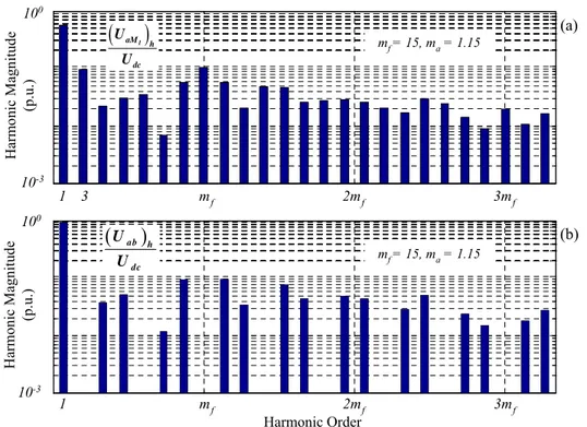
Figure 3-37: Voltage waveforms of the 7L-SC2LHB VSC: (a) reference and triangular signals, (b) output phase voltage Uan, (c) output line-to-line voltage Uab, (d) output load-phase voltage Uan´ (mf = 15)
Figure 3-38: Harmonic spectrum of the phase voltage (a) and line-to-line voltage (b) of the 7L-SC2LHB VSC
Figure 3-39: The 9L-SC2LHB Voltage Source Converter
Figure 3-40: Pulse width modulation for the 9L-SC2LHB VSC: (a) control signals Ucon,a and triangular signals Utri,Li and Utri,Ri, (b) gate signals (mf = 3)
Figure 3-41: Voltage waveforms of the 9L-SC2LHB VSC: (a) reference and triangular signals, (b) output phase voltage Uan´, (c) output line-to-line voltage Uab, (d) output load-phase voltage Uan (mf = 15)
(b) of the 9L-SC2LHB VSC
Figure 3-43: NL-SC3LHB VSC with p series 3L-H-Bridge cells per phase Figure 3-44: Five-level SC3LHB diode clamped topology (5L-SC3LHB)
Figure 3-45: Voltage waveforms of the 5L-SC3LHB VSC: (a) control signal Ucon and triangular signals, (b) a1-leg gate signals, (c) a1-leg phase voltage, (d) a2-leg gate signals, (e) a2-leg phase voltage, (f) converter output voltage
Figure 3-46: Harmonic spectrum of the 5L-SC3LHB VSC
Figure 3-47: Number of total components required in the multi-level converter as a function of the number of phase voltage levels
Figure 4-1: Block diagram of Medium Voltage Drives: (a) NPC and FLC VSCs, (b) SCHB VSC
Figure 4-2: Standard load model for one-phase and three-phase Figure 4-3: Standard three-phase utility grid model
Figure 4-4: The ideal circuit symbol of the IGBT
Figure 4-5: The steady state equivalent thermal circuit diagram: (a) general model, (b) Infineon model
Figure 4-6: Characteristics of current sharing for two connected modules in parallel
Figure 4-7: Approximation characteristics based on the curve-fitting method: (a) IGBT/Diode on-state characteristics, (b) IGBT turn-on and IGBT/Diode turn-off switching energy (FZ800R33KF2C IGBT-module from Eupec, UCE = 1800V, Tj,max = 125°C)
Figure 4-8: Equivalent circuit of a capacitor
Figure 4-9: Circuit diagram of the standard six-pulse diode rectifier Figure 4-10: Multi-pulse phase-shift transformer
Figure 4-11: 24-pulse phase-shift transformer models: (a) Zdy, (b) Dzz
Figure 4-12: Investigated zigzag coupling configurations: (a) Delta-zigzag-zigzag configuration (Dzz), (b) Zigzag-delta-star configuration (Zdy) used by the industry
Figure 4-13: Windings position for positive (a), and negative (b) phase shift of Dzz configuration
Figure 4-14: Windings position for positive (a), and negative (b) phase shift of Zdy configuration
Figure 4-15: Equivalent electrical circuit of a linear 3-winding transformer Figure 4-16: The model of a 12-pulse transformer
Figure 4-17: 24-Pulse-Diode-Rectifier with serial connections and Dzz configuration Figure 4-18: 24-Pulse-Diode-Rectifier with serial connections and Zdy configuration
Figure 4-19: Utility grid current and its harmonic spectrum for the 24-pulse transformer (a, b), primary winding currents and their harmonic spectrum for the 12-pulse transformer (c, d), and secondary winding currents and their harmonic spectrum for the 12-pulse transformer (e, f)
Figure 4-20: Primary and secondary winding currents of the 24-pulse transformer
Figure 4-21: DC link voltage and its harmonic spectrum (a, b), and dc link current and its harmonic spectrum, Idc = 710A, fC = 750Hz
Figure 4-22: 24-Pulse-Diode-Rectifier with independent connections: (a) Dzz configuration, and (b) Zdy configuration
Figure 4-23: Utility grid current and its harmonic spectrum for the 24-pulse transformer (a, b), primary winding currents and their harmonic spectrum for the 12-pulse transformer (c, d), and secondary winding currents and their harmonic spectrum for the 12-pulse transformer (e, f)
Figure 4-24: Primary and secondary winding currents of the 24-pulse transformer Figure 4-25: DC link voltage and its harmonic spectrum, fC= 750Hz
Figure 4-26: DC link current and its harmonic spectrum, Idc = 471A, fC = 750Hz Figure 5-1: Iterative design approach to the power semiconductor design
Figure 5-2: Iterative design approach to calculate the maximum converter output power SC,max and the semiconductor utilization (Tj = Tj,max, SS = const., fC = const.)
Figure 5-3: Iterative design approach to calculate the maximum carrier frequency (Tj = Tj,max, SS = const., SC = const.)
Figure 5-4: Iterative design approach to calculate the converter output power and losses (Tj = Tj,max, SS = const., f1Cb = const.)
Figure 5-5: Iterative design approach to calculate the maximum carrier frequency (Tj = Tj,max, SC = const., η = ηref≈ const.)
Figure 5-6: The dc link voltage ripple ∆UC and the dc link stored energy EC as functions of the dc link capacitance for the 3L-NPC VSC (Ull,rms,1 = 4.16kV, Iph,rms,1 = 600A, cos ϕ = 0.9, Udc = 6118V)
Figure 5-7: 24-pulse diode rectifier configurations (a) series configuration uses for the 3L-NPC VSC, (b) separate configuration uses for the9L-SCHB VSC
Figure 5-8: Voltage and power ranges of the selective medium voltage drives (Iph,rms,1 = 600A), (6.5kV/600A: FZ600R65KF1, 4.5kV/600A: CM600HB-90H, 3.3kV/800A: FZ800R33KF2, 2.5kV/1000A: FZ1000R25KF1, 1.7kV/600A: FZ600R17KE3) Figure 6-1: Converter semiconductor losses and efficiencies as functions of the phase current
for the investigated output voltage classes (fC = 450Hz, ma = 1.15, cosϕ = 0.9): (a) Ull,rms,1 = 2.3kV, (b) Ull,rms,1 = 3.3kV, and (c) Ull,rms,1 = 4.16kV (6.5kV/600A: FZ600R65KF1, 4.5kV/600A: CM600HB-90H, 3.3kV/800A: FZ800R33KF2, 2.5kV/1000A: FZ1000R25KF1, 1.7kV/600A: FZ600R17KE3)
Figure 6-2: Converter semiconductor loss distribution at constant carrier frequency (fC = 450Hz, ma = 1.15, cosϕ = 0.9, Iph,rms,1 = 600A) (a) Ull,rms,1 = 2.3kV, (b) Ull,rms,1 = 3.3kV, (c) Ull,rms,1 = 4.16kV (6.5kV/600A: FZ600R65KF1, 4.5kV/600A: CM600HB-90H, 3.3kV/800A: FZ800R33KF2, 2.5kV/1000A: FZ1000R25KF1, 1.7kV/600A: FZ600R17KE3)
Figure 6-3: Harmonic spectrum of line-to-line output voltage at constant carrier frequency (fC = 450Hz, fo = 50Hz, ma = 1.15, f1Cb,3L-NPC = 450Hz, f1Cb,3L-FLC = 900Hz, f1Cb,4L-FLC = 1350Hz, f1Cb,5L-SC2LHB = 1800Hz, f1Cb,7L-SC2LHB = 2700Hz, f1Cb,9L-SC2LHB = 3600Hz) (6.5kV/600A: FZ600R65KF1, 4.5kV/600A: CM600HB-90H, 3.3kV/800A:
FZ800R33KF2, 2.5kV/1000A: FZ1000R25KF1, 1.7kV/600A: FZ600R17KE3) Figure 6-4: Converter semiconductor losses and efficiencies as functions of the carrier
frequency for the investigated output voltage classes: (a) Ull,rms,1 = 2.3kV, (b) Ull,rms,1 = 3.3kV, and (c) Ull,rms,1 = 4.16kV (fC = 450Hz, Iph,rms,1 = 600A, ma = 1.15, cosϕ = 0.9) (6.5kV/600A: FZ600R65KF1, 4.5kV/600A: CM600HB-90H, 3.3kV/800A: FZ800R33KF2, 2.5kV/1000A: FZ1000R25KF1, 1.7kV/600A: FZ600R17KE3)
Figure 6-5: Converter semiconductor loss distribution at maximum carrier frequency (fo = 50Hz, ma = 1.15, cosϕ = 0.9, Iph,rms,1 = 600A, fC = 450Hz), (fC,3L-NPC = 450Hz, f C,3L-FLC,2.3kV = 880Hz, fC,3L-FLC,3.3kV = 635Hz, fC,3L-FLC,4.16kV = 595Hz, fC,4L-FLC,2.3kV = 250Hz, fC,4L-FLC,3.3kV = 790Hz, fC,4L-FLC,4.16kV = 850Hz, fC,5L-SC2LHB = 1585Hz, f C,7L-SC2LHB = 1300Hz, fC,9L-SC2LHB =3450Hz) (6.5kV/600A: FZ600R65KF1, 4.5kV/600A: CM600HB-90H, 3.3kV/800A: FZ800R33KF2, 2.5kV/1000A: FZ1000R25KF1, 1.7kV/600A: FZ600R17KE3)
Figure 6-6: Harmonic spectrum of line-to-line voltage at maximum carrier frequency (f1Cb,3L-NPC = 450Hz, f1Cb,3L-FLC,2.3kV = 1760Hz f1Cb,4L-FLC,2.3kV = 750Hz f1Cb,5L-SC2LHB = 6340Hz, fo = 50Hz, fC = 450Hz, ma = 1.15, cosϕ = 0.9, Iph,rms,1 = 600A) (3.3kV/800A: FZ800R33KF2, 2.5kV/1000A: FZ1000R25KF1, 1.7kV/600A: FZ600R17KE3) Figure 6-7: Harmonic spectrum of line-to-line voltage at maximum carrier frequency (f1Cb,3L-NPC
= 450Hz, f1Cb,3L-FLC,3.3kV = 1270Hz, f1Cb,4L-FLC,3.3kV = 2370Hz, f1Cb,7L-SC2LHB = 7800Hz, fo = 50Hz, fC = 450Hz, ma = 1.15, cosϕ = 0.9, Iph,rms,1 = 600A) (4.5kV/600A: CM600HB-90H, 3.3kV/800A: FZ800R33KF2, 1.7kV/600A: FZ600R17KE3)
Figure 6-8: Harmonic spectrum of line-to-line voltage at maximum carrier frequency (f1Cb,3L-NPC = 450Hz, f1Cb,3L-FLC,4.16kV = 1190Hz, f1Cb,4L-FLC,4.16kV = 2550Hz, f1Cb,9L-SC2LHB = 27600Hz, fo = 50Hz, fC = 450Hz, ma = 1.15, cosϕ = 0.9, Iph,rms,1 = 600A) (6.5kV/600A: FZ600R65KF1, 4.5kV/600A: CM600HB-90H, 1.7kV/600A: FZ600R17KE3)
Figure 6-9: Converter semiconductor losses as functions of the phase current for the investigated output voltage classes: (a) Ull,rms,1 = 2.3kV, (b) Ull,rms,1 = 3.3kV, and (c) Ull,rms,1 = 4.16kV (fC,3L-NPC = 450Hz, fC,3L-FLC = 225Hz, fC,4L-FLC = 150Hz, f C,5L-SC2LHB = 112.5Hz, fC,7L-SC2LHB = 75Hz, fC,9L-SC2LHB = 56.25Hz, fo = 50Hz, f1Cb = 450Hz, ma = 1.15, cosϕ = 0.9, Iph,rms,1 = 600A), (6.5kV/600A: FZ600R65KF1, 4.5kV/600A: CM600HB-90H, 3.3kV/800A: FZ800R33KF2, 2.5kV/1000A: FZ1000R25KF1, 1.7kV/600A: FZ600R17KE3)
Figure 6-10: Converter semiconductor loss distribution at constant frequency of the first carrier band (fC = f1Cb = 450Hz, ma = 1.15, cosϕ = 0.9, Iph,rms,1 = 600A): (a) Ull,rms,1 = 2.3kV, (b) Ull,rms,1 = 3.3kV, (c) Ull,rms,1 = 4.16kV (fC,3L-NPC = 450Hz, fC,3L-FLC = 225Hz, fC,4L-FLC = 150Hz, fC,5L-SC2LHB = 112.5Hz, fC,7L-SC2LHB = 75Hz, fC,9L-SC2LHB = 56.25Hz, fo = 50Hz, f1Cb = 450Hz, ma = 1.15, cosϕ = 0.9, Iph,rms,1 = 600A), (6.5kV/600A: FZ600R65KF1, 4.5kV/600A: CM600HB-90H, 3.3kV/800A: FZ800R33KF2, 2.5kV/1000A: FZ1000R25KF1, 1.7kV/600A: FZ600R17KE3) Figure 6-11: Harmonic spectrum of line-to-line voltage at constant frequency of the first carrier
band (fC,3L-NPC = 450Hz, fC,3L-FLC = 225Hz, fC,4L-FLC = 150Hz, fC,5L-SC2LHB = 112.5Hz, fC,7L-SC2LHB = 75Hz, fC,9L-SC2LHB = 56.25Hz, fo = 50Hz, f1Cb = 450Hz, ma = 1.15, cosϕ = 0.9, Iph,rms,1 = 600A), (6.5kV/600A: FZ600R65KF1, 4.5kV/600A:
CM600HB-90H, 3.3kV/800A: FZ800R33KF2, 2.5kV/1000A: FZ1000R25KF1, 1.7kV/600A: FZ600R17KE3)
Figure 6-12: Average junction temperature of IGBTs and diodes (Udc,n = 6118V, ma = 1.15, cosϕ = 1, Th = 80°C) (a) 3L-NPC VSC (Eupec 6.5kV/740.4A IGBT, Iph,max = 600A, SC = 4.32MVA, fC = 450Hz) (b) 3L-FLC VSC (Eupec 6.5kV/863.4A IGBT, Iph,max = 919A, SC = 6.62MVA, fC = 225Hz) (c) 4L-FLC VSC (Mitsubishi 4.5kV/832A IGBT, Iph,max = 1061A, SC = 7.64MVA, fC = 150Hz) (d) 9L-SCHB VSC (Eupec 1.7kV/825.8A IGBT, Iph,max = 891A, SC = 6.42MVA, fC = 56.25Hz) Figure 6-13: Loss distribution (a), efficiency (b), and relative installed switch power (c), (Sc =
4.32MVA, Iph,rms,1 = 600A, fo = 50Hz, ma = 1.15, cos ϕ = 0.9, Tjmax = 125°C, f C,3L-NPC-6.5kV = 450Hz, fC,3L-NPC-3.3kV = 1250Hz, fC,3L-FLC-6.5kV = 475Hz, fC,3L-FLC-3.3kV = 650Hz, fC,4L-FLC-4.5kV = 610Hz, fC,9LSC2LHB-1.7kV = 1125Hz), (6.5kV/600A: FZ600R65KF1, 4.5kV/600A: CM600HB-90H, 3.3kV/800A: FZ800R33KF2, 2.5kV/1000A: FZ1000R25KF1, 1.7kV/600A: FZ600R17KE3)
Figure 6-14: Flying capacitor current (a) and voltage ripple (b) of a 3L-FLC VSC as functions of the modulation index and phase shift (Iph,rms,1 = 600A, fC,3L-FLC = 1200Hz, C = 770µF)
Figure 6-15: Flying capacitor current (a) and voltage ripple (b) of a 4L-FLC VSC as functions of the modulation index and phase shift (Iph,rms,1 = 600A, fC,4L-FLC = 1200Hz, C1,2 = 518µF)
Figure 6-16: Harmonic spectrum of line-to-line voltage at constant efficiency (Iph,rms,1 = 600A, fo = 50Hz, ma = 1.15, cos ϕ = 0.9, Tjmax = 125°C, fC,3L-NPC-6.5kV = 450Hz, f C,3L-NPC-3.3kV = 1250Hz, fC,3L-FLC-6.5kV = 475Hz, fC,3L-FLC-3.3kV = 650Hz, fC,4L-FLC-4.5kV = 610Hz, fC,9LSC2LHB-1.7kV = 1125Hz)
Figure 6-17: Semiconductor loss distribution and relative installed switch power occurring at line-to-line output voltages of 2.3kV, 3.3kV, 4.16kV, and 6kV at different switching frequencies of 450Hz, 750Hz, and 1050Hz (Iph,rms,1 = 600A, fo = 50Hz, ma = 1.15, cos ϕ = 0.9, Tjmax = 125°C), (6.5kV/600A: FZ600R65KF1, 4.5kV/600A: CM600HB-90H, 3.3kV/800A: FZ800R33KF2, 2.5kV/1000A: FZ1000R25KF1, 1.7kV/600A: FZ600R17KE3)
Figure 6-18: The effective, average, and ripple capacitor current as a function of the modulation index and load angle in the 3L-NPC VSC according to Figure 3-6: (a-c) (idc2,eff,max/iph,peak = 85.6% at φ = ±180°, 0° and ma = 1.15), (idc2,avg,max/iph,peak = 80.3% at φ = 0° and ma = 1.15), (idc2,rip,max/iph,peak = 45.8% at φ = ±180°, 0° and ma = 0.6), and in the 9L-SC2LHB VSC according to Figure 3-39 (d-f).(idc21,eff,max/iph,peak = 68.7% at φ = ±180°, 0° and ma = 1.15), (idc21,avg,max/iph,peak = 57.5% at φ = 0° and ma = 1.15), (idc21,rip,max/iph,peak = 54.3% at φ = ±90°, and ma = 1.15), (iph,rms,1 = 600A, fC = 750Hz, fo = 50Hz)
Figure 6-19: (a, b): Utility grid phase current and its harmonic spectra in the 3L-NPC VSC, (c, d): transformer primary phase currents of the 12-pulse transformer and their harmonic spectra in the 3L-NPC VSC, (e, f): transformer secondary phase currents of the 12-pulse transformer and their harmonic spectra in the 3L-NPC VSC (E = 6J/kVA, C1 = C2 = 2.77mF, fC = 750Hz, fo = 50Hz, ma = 0.6, Vll,rms,1 = 4.16kV, Iph,rms,1 = 600A, cosφ = 0.9)
Figure 6-20: (a, b): Utility grid phase current and its harmonic spectra in the 3L-NPC VSC, (c, d): transformer primary phase currents of the 12-pulse transformer and their
harmonic spectra in the 3L-NPC VSC, (e, f): transformer secondary phase currents of the 12-pulse transformer and their harmonic spectra in the 3L-NPC VSC (E = 12J/kVA, C1 = C2 = 5.54mF, fC = 750Hz, fo = 50Hz, ma = 0.6, Vll,rms,1 = 4.16kV, Iph,rms,1 = 600A, cosφ = 0.9)
Figure 6-21: (a, b): Utility grid phase current and its harmonic spectra in the 9L-SC2LHB VSC, (c, d): transformer primary phase currents of the 12-pulse transformer and their harmonic spectra in the 9L-SC2LHB VSC, (e, f): transformer secondary phase currents of the 12-pulse transformer and their harmonic spectra in the 9L-SC2LHB VSC (E = 12J/kVA, C1 = C2 = 14.8mF, fC = 750Hz, fo = 50Hz, ma = 1.15, Vll,rms,1 = 4.16kV, Iph,rms,1 = 600A, cosφ = 0.9)
Figure 6-22: (a, b): Utility grid phase current and its harmonic spectra in the 9L-SC2LHB VSC, (c, d): transformer primary phase currents of the 12-pulse transformer and their harmonic spectra in the 9L-SC2LHB VSC, (e, f): transformer secondary phase currents of the 12-pulse transformer and their harmonic spectra in the 9L-SC2LHB VSC (E = 34J/kVA, C1 = C2 = 44mF, fC = 750Hz, fo = 50Hz, ma = 1.15, Vll,rms,1 = 4.16kV, Iph,rms,1 = 600A, cosφ = 0.9)
Figure 6-23: (a, b): DC link voltage ripple and its harmonic spectra in the 3L-NPC VSC, (c, d): dc link current and its harmonic spectra, (e, f): capacitor voltage ripples and their harmonic spectra in the 3L-NPC VSC (E = 6J/kVA, C1 = C2 = 2.77mF, fC = 750Hz, fo = 50Hz, ma = 0.6, Vll,rms,1 = 4.16kV, Iph,rms,1 = 600A, cosφ = 0.9)
Figure 6-24: (a, b): DC link voltage ripple and its harmonic spectra in the 3L-NPC VSC, (c, d): dc link current and its harmonic spectra in the 3L-NPC VSC, (e, f): capacitor voltage ripples and their harmonic spectra in the 3L-NPC VSC (E = 12J/kVA, C1 = C2 = 5.54mF, fC = 750Hz, fo = 50Hz, ma = 0.6, Vll,rms,1 = 4.16kV, Iph,rms,1 = 600A, cosφ = 0.9)
Figure 6-25: (a, b): DC link voltage ripple and its harmonic spectra in the 9L-SC2LHB VSC, (c, d): dc link current and its harmonic spectra in the 9L-SC2LHB VSC, (e, f): phase output voltage and its harmonic spectra in the 9L-SC2LHB VSC (E = 12J/kVA, C1 = C2 = 14.8mF, fC = 750Hz, fo = 50Hz, ma = 1.15, Vll,rms,1 = 4.16kV, Iph,rms,1 = 600A, cosφ = 0.9)
Figure 6-26: (a, b): DC link voltage ripple and its harmonic spectra in the 9L-SC2LHB VSC, (c, d): dc link current and its harmonic spectra in the 9L-SC2LHB VSC, (e, f): phase output voltage and its harmonic spectra in the 9L-SC2LHB VSC (E = 34J/kVA, C1 = C2 = 44mF, fC = 750Hz, fo = 50Hz, ma = 1.15, Vll,rms,1 = 4.16kV, Iph,rms,1 = 600A, cosφ = 0.9)
Figure 6-27: (a, b): Capacitor current ripples and their harmonic spectra in the 3L-NPC VSC, (c, d): phase-midpoint output voltage and its harmonic spectra in the 3L-NPC VSC, (e, f): phase output load currents and their harmonic spectra in the 3L-NPC VSC (E = 6J/kVA, C1 = C2 = 2.77mF, fC = 750Hz, fo = 50Hz, ma = 0.6, Vll,rms,1 = 4.16kV, Iph,rms,1 = 600A, cosφ = 0.9)
Figure 6-28: (a, b): Capacitor current ripples and their harmonic spectra in the 3L-NPC VSC, (c, d): phase-midpoint output voltage and its harmonic spectra in the 3L-NPC VSC, (e, f): phase output load currents and their harmonic spectra in the 3L-NPC VSC (E = 12J/kVA, C1 = C2 = 5.54mF, fC = 750Hz, fo = 50Hz, ma = 0.6, Vll,rms,1 = 4.16kV, Iph,rms,1 = 600A, cosφ = 0.9)
List of Tables
Table 2-1: Overview of available industrial medium voltage drives on the market Table 2-2: Device rating and package types of typical MV power semiconductors Table 3-1: Switch positions for each phase of the two-level VSC
Table 3-2: Conduction losses in the two-level VSC Table 3-3: Switching losses in the two-level VSC
Table 3-4: Switch positions for one phase of the three-level NPC VSC Table 3-5: Conduction losses in the 3L-NPC VSC
Table 3-6: Switching losses in the 3L-NPC VSC
Table 3-7: Switch positions for one phase of the three-level FLC VSC Table 3-8: Conduction losses in the three -level FLC VSC
Table 3-9: Switching losses in the three-level FLC VSC
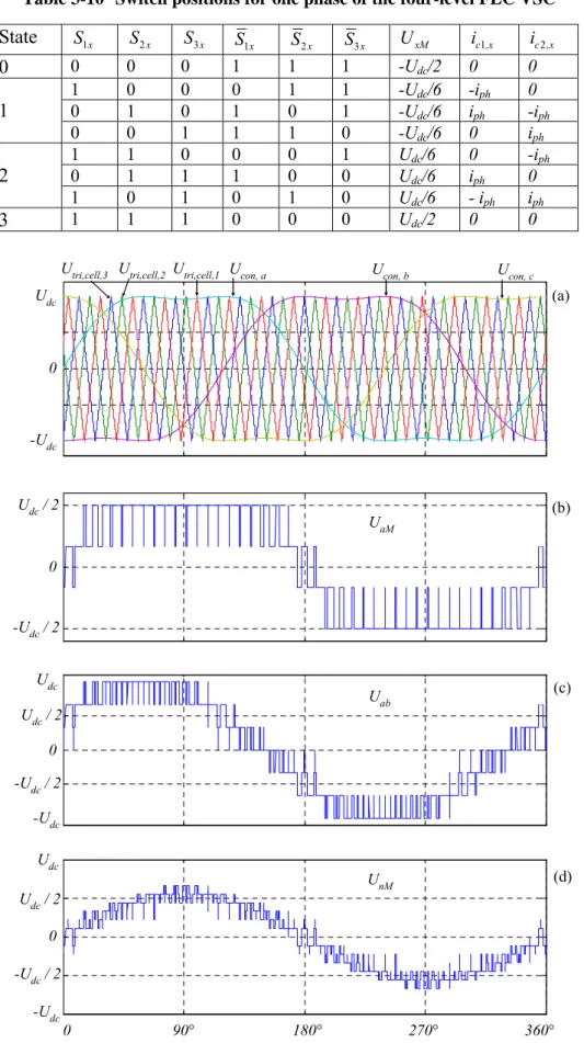
Table 3-10:Switch positions for the one phase of the four-level FLC VSC Table 3-11:Switch positions for single-phase H-bridge cell
Table 3-12:Conduction losses in the single-phase full-Bridge converter Table 3-13:Switching losses in the single-phase full-Bridge converter Table 3-14:Quantities comparison of the SC2LHB VSC
Table 3-15:Switch positions for the 5L-SC2LHB VSC
Table 3-16:The output voltage levels of the 5L-SC2LHB VSC
Table 3-17:Number of redundancies in each phase voltage level of the 7L-SC2LHB VSC Table 3-18:The output voltages and their corresponding levels of the 7L-SC2LHB VSC Table 3-19:The output voltages and their corresponding levels of the 9L-SC2LHB VSC Table 3-20:Switch positions for the 3L-H-Bridge converter
Table 3-21:Conduction losses in the 3L-H-Bridge converter Table 3-22:Switching losses in the 3L-H-Bridge converter
Table 3-23:Comparison of power component requirements for multi-level topologies Table 4-1: Fitting parameters and thermal resistances of medium voltage IGBTs/Diodes Table 4-2: Thermal resistance of the IGBT module:FZ600R65KF1
Table 4-3: Harmonic current and their phase angles in 24-pulse transformers Table 4-4: The necessary input data of the 12-pulse phase-shift transformer
Table 4-5: The secondary quantity parameters for the 24-pulse transformer with Zdy connection
Table 4-6: The designing parameters for the 24-pulse transformer with Zdy connection Table 5-1: Critical operating points for the determination of the power semiconductor current
ratings (stationary thermal design) for all considered topologies Table 5-2: Converter data (Output phase current Iph,rms,1 = 600A)
Table 5-3: Power semiconductor devices
Table 5-4: The converter specifications for medium voltage converters
Table 6-1: Power semiconductor design for Iph,rms,1 = 600A, fC = 450Hz / 1000Hz
Table 6-2: Maximum phase current and apparent converter output power for constant carrier frequency (Iph,rms,1 = 600A, ma = 1.15, cosϕ = 0.9)
Table 6-3: Maximum carrier frequency for constant apparent converter output power and constant installed switch power (Iph,rms,1 = 600A, ma = 1.15, cosϕ = 0.9)
Table 6-4: Maximum phase current and apparent converter output power for constant carrier frequency of the first carrier band and installed switch power (Iph,rms,1 = 600A, f1Cb = 450Hz / 1000Hz, ma = 1.15, cosϕ = 0.9)
Table 6-5: Converter voltage and semiconductor specifications for a constant converter power and carrier frequency (Ull,rms,1 = 4.16kV, Iph,rms,1 = 600A, SC = 4.32MVA, fC = 450Hz, Tj,max = 125°C)
Table 6-6: Carrier and harmonic carrier band frequencies, capacity of flying capacitors and installed switch power for a converter efficiency of about 99% (Ull,rms,1 = 4.16kV, Iph,rms,1 = 600A, SC = 4.32MVA)
1.
INTRODUCTION
The development of new high power semiconductors such as 3.3kV, 4.5kV, and 6.5kV Insulated Gate Bipolar Transistors (IGBTs), and 4.5kV to 5.5kV Integrated Gate Commutated Thyristors (IGCTs), and improved converter designs have led to a drastic increase of the market share of Pulse-Width-Modulated (PWM) controlled Voltage Source Converters (VSC) [21]. Despite a price reduction of Gate Turn-Off Thyristors (GTOs) by a factor of two to three over the last five years, also conventional GTO Voltage Source Converters and Current Source Converters (CSC) are increasingly replaced by PWM Voltage Source Converters with IGCTs or IGBTs in traction and industry applications [21].
Today the two-level Voltage Source Converter (2L-VSC) applying IGBTs is clearly the dominating converter topology in traction applications (low, medium, and high power propulsion) and the three-level Neutral Point Clamped Voltage Source Converter (3L-NPC VSC) is mostly applied in industrial medium voltage converters. The 2L-VSC and the 3L-NPC VSC offer technical advantages like a simple power part, a low component count, and straightforward protection and modulation schemes. On the other hand, the hard-switching transients of the power semiconductors at high commutation voltage cause high switching losses and a poor harmonic spectrum which produces additional losses in the machine. Further problems are created by over-voltages in cables and machines as well as bearing currents due to the steep-switching transients [5], [21], [121].
Multi-level converters (MLCs) have been receiving attention in the recent years and have been proposed as the best choice in a wide variety of medium voltage (MV) applications [47]. They enable a commutation at substantially reduced voltages and an improved harmonic spectrum without a series connection of devices, which is the main advantage of a multi-level structure. Other advantages of these topologies are better output voltage quality, reduced electromagnetic interference (EMI) problems, and lower overall losses in some cases. However, today they have a limited commercial impact due to their disadvantages such as high control complexity and increased power semiconductor count compared to the 2L-VSC and the 3L-NPC VSC.
There is a large variety of power semiconductors (e.g. IGBTs, GTOs, IGCTs) and converter topologies (e.g. 2L-VSC, 3L-NPC VSC, 3L-FLC VSC, 4L-FLC VSC, and SCHB VSCs). However, today there is no comparative analysis of the different converter topologies. Therefore, the objective of this thesis is a detailed comparison of state-of-the-art 2L-VSC, 3L-NPC VSC, and different multi-level VSCs (e.g. 3L-FLC VSC, 4L-FLC VSC, 5L-, 7L-, and 9L-SC2LHB VSCs) for medium voltage converters. On the basis of the application requirements, different ML converter structures are designed, simulated, and evaluated. The development of design tools based on state-of-the-art converters and semiconductors, which enable the dimensioning of power semiconductors, dc link capacitors, and transformers; are one major part of this thesis. Finally, the amount of active and passive components, the modulation, losses, and efficiency of aforementioned converters are calculated and compared.
The thesis is arranged in seven main chapters: This introduction is followed by an overview of medium voltage converter topologies, including medium voltage power semiconductors and modulations in chapter 2.
Chapter 3 presents the basic structure and function of voltage source converter topologies. Based on the requirements for MV applications, advantages and disadvantages of the topologies are discussed.
One of the main parts of this thesis is the modelling and simulation of the different multi-level converters. The dimensioning and design of power semiconductors, dc link capacitors, and isolation transformers are developed in chapter 4.
The basic converter data for a converter comparison, including the IGBTs, modulation, switching frequency, and state of the art are described in chapter 5.
The comparison of the different converter topologies is performed in chapter 6 for 3L-NPC VSC, 3L-FLC VSC, 4L-FLC VSC, and 5L-, 7L-, 9L-, and 11L-SCHB VSCs on the basis of the state-of-the-art 1.7kV, 2.5kV, 3.3kV, 4.5kV, and 6.5kV IGBTs for 2.3kV, 3.3kV, 4.16kV, and 6kV medium voltage converters. As a result, the converter losses, the semiconductor loss distribution, the converter efficiency, harmonic spectrum analysis, and the installed switch power of the different converter topologies are compared in this chapter.
2.
OVERVIEW OF MEDIUM VOLTAGE CONVERTER TOPOLOGIES
2.1.State of the Art in Medium Voltage Converters
Multi-level voltage source converters have been studied intensively for high-power applications [44], [53], [87], [88]. Standard drives for medium voltage industrial applications have become available since the mid-1980s [27], [82], [83], [129]. These converters synthesize higher output voltage levels with a better harmonic spectrum and less motor winding insulation stress. However, the reliability and efficiency of the converter are reduced due to an increasing number of devices.
“Today there is a large variety of converter topologies for Medium Voltage Drives (MVD). For low and medium power industrial applications (e.g. S = 300kVA - 30MVA) the majority of the drive manufacturers offer different topologies of Voltage Source Converters: Two-Level Voltage Source Converters (2L-VSC) (e.g. Alstom), Three-Level Neutral Point Clamped Voltage Source Converters (3L-NPC VSC) (e.g. ABB, Alstom, Siemens), Four-Level Flying Capacitor Voltage Source Converters (4L-FLC VSC) (e.g. Alstom: SYMPHONY [80]) and Series Connected H-Bridge Voltage Source Converters (SCHB VSC) (Robicon [81], [139]). One manufacturer (Allen Bradley) still offers self-commutated current source inverters (CSI). While 4.5kV, 6kV and 6.5kV IGCTs are mainly used in 3L-NPC VSCs and CSIs respectively; 2.5kV, 3.3kV, 4.5kV and 6.5kV High Voltage IGBTs (HV-IGBTs) are applied in 2L-VSCs, 3L-NPC VSCs and 4L-FLC VSCs. In contrast, 1.2kV and 1.7kV Low Voltage IGBTs (LV-IGBTs) are usually applied in SCHB VSCs [94]”.
Among the high-power multi-level converters, three topologies have been successfully implemented as standard products for medium voltage industrial drives: the Three-Level Neutral Point Clamped Voltage Source Converter (3L-NPC VSC) [82], [83], the Four-Level Flying Capacitor Voltage Source Converters (4L-FLC VSC) [80], and the Series Connected H-Bridge Voltage Source Converters (SCHB VSC) [27], [129].
In medium voltage applications, the 3L-NPC topology has been accepted by several large manufacturers. ABB is using this topology in both their ACS 1000 [83] and ACS 6000 series, in
a voltage and power range of 2.3kV-4.16kV and 315kVA-27MVA [154]. Siemens’ SIMOVERT MV [155] is also utilising this topology with output voltages from 2.3kV to 6.6kV and a power range from 660kVA to 9MVA. Not only European but also Asian vendors, such as Mitsubishi, employ the 3L-NPC converter [48].
The NPC topology uses high-voltage blocking devices with a relatively low switching frequency capability. This topology has a simple circuit but it needs a large inductive-capacitive (LC) output filter to operate standard motors.
The 4L-FLC VSC is attractive if a very high switching frequency, a low harmonic distortion, and a small output filter or a high output voltage is required [25].
The SCHB topology uses low-voltage blocking devices (e.g. 1700V IGBTs) with a high switching frequency capability. It typically consists of three to six equal H-bridge cells per phase, which results in a seven- to thirteen-level output voltage waveform. An input isolation transformer feeds each of the H-bridges via its own three-phase winding and full-bridge
diode-rectifier. To obtain a high pulse number at the primary side, secondary transformer windings in star, delta, zigzag, and combinations are used. This topology has excellent utility grid current and output voltage waveforms. However, the cost of the complex input transformer and the high number of semiconductor devices with their control equipment are its drawbacks. The disadvantages of both topologies can be limited by using a hybrid asymmetric multi-level converter which is constructed by combining the SCHB with the NPC topologies [133], [134]. This combination produces more output voltage levels with the same number of components than a symmetric multi-level converter. The first H-bridge cells of each phase in the SCHB topology are replaced by a leg of the NPC converter. Although an H-bridge cell and a leg of the NPC converter provide the same output voltage level, the hybrid asymmetric multi-level topology requires a smaller number of separate dc sources and H-bridge cells for the same output voltage levels [85], [86]. This leads to a further simplification of the feeding transformer and rectifiers [84]. This topology can be operated with a low or high switching frequency for high- or low-voltage applications. However, the need for a complex input transformer remains and its control would be complicated due to its structure, so that it is not commercially offered on the market.
Table 2-1 summarizes the available industrial medium voltage drive applications offered by drive manufactures [28]. The voltage source converter topology applying IGBTs and IGCTs are offered by the majority of manufactures. The medium voltage drives cover power ratings from 0.2MW to 40MW at the medium voltage level of 2.3kV to 13.8kV [9], [28]. These drives are used in various applications such as traction [21], electric power, and other industries [35]. The medium voltage traction converters are mostly fed by a single-phase ac line using a low-frequency transformer (e.g. 15kV 16 3 Hz or 25kV 50Hz) [21], [38], [39]. The feeding of 2 some traction converters by dc mains is also possible, but due to the large variations of the dc voltages of -30% to +40%, such applications are complicated [21].
Figure 2-1 represents the most important power converters on the market and their rated voltages and powers today [14], [28].
Table 2-1 Overview of available industrial medium voltage drives on the market [28], [75]
Manu-facturer Type Power (MVA) Voltage (kV) Topology Semiconductor Robicon Perfect Harmony 0.3-31 2.3-13.8 ML-SCHB-VSC LV IGBT
Allen
Bradley Power Flex 7000 0.15-6.7
2.3, 3.3, 4.16, 6.6 CSI IGCT Masterdrive MV 0.66-9.1 2.3, 3.3, 4.16, 6, 6.6 3L-NPC-VSC HV IGBT Siemens Masterdrive ML2 5-30 3.3 3L-NPC-VSC IGCT ACS 1000 0.3-5 2.3, 3.3, 4 3L-NPC-VSC IGCT ACS 5000 5.2-24 6, 6.6, 6.9 ML-SCHB-VSC IGCT ABB ACS 6000 3-27 3, 3.3 3L-NPC-VSC IGCT VDM 5000 1.4-7.2 2.3, 3.3, 4.2 2L-VSC IGBT VDM 6000 0.3-8 2.3, 3.3, 4.2 4L-FLC-VSC IGBT Alstom VDM 7000 7-9.5 3.3 3L-NPC-VSC GTO Dura-Bilt5 MV 0.3-2.4 4.16 3L-NPC-VSC IGBT General
Figure 2-2 illustrates two examples of medium voltage drives: Figure 2-2a shows a medium voltage drive using an IGBT-based 3L-NPC inverter (SIMOVERT [9]). The standardized output power range extends for motors from about 0.2MW up to more than 7MW [150]. Figure 2-2b shows a 4.16kV, 7.5MW SCHB inverter with five identical IGBT power cells which generate 21 levels at the line-to-line output voltage (ASI Robicon [9]).
Figure 2-1 Application ranges of commercially available power semiconductors [14], [28]
Figure 2-2 IGBT-based inverter fed medium voltage drives: (a) 3L-NPC, (b) SCHB [9], [75]
2.2.State of the Art in Medium Voltage Power Semiconductors
Recent technology advances in power electronics have been made by improvements in controllable power semiconductor devices. Figure 2-3 and Figure 2-4 summarize the most important power semiconductors on the market and their rated voltages and currents today [14], [21]. The device characteristics for medium voltage power semiconductors are shown in Table 2-2 [28].
Metal Oxide Semiconductor Field Effect Transistors (MOSFET) and IGBTs have replaced Bipolar Junction Transistors (BJT) almost completely. A remarkable development in MOSFETs took place during the last years. Nowadays MOSFETs are available up to a maximum switch power of about 100kVA [21].
Various new concepts of MOS-controlled thyristors such as the MOS-controlled thyristor (MCT) and the MOS turn-off thyristor (MTO) have been presented but they do not have any commercial applications.
Conventional GTOs are available with a maximum device voltage of 6kV in traction and industrial converters (Table 2-2) [21], [28]. The high on state current density, the high blocking voltages, and the possibilities to integrate an inverse diode are considerable advantages of these devices. However, the requiring of bulky and expensive snubber circuits [92], [93] as well as the complex gate drive are the reasons that GTOs are being replaced by IGCTs and Gifts [21], [28]. Like GTOs, IGCTs are offered only as a presspack device. The symmetrcial IGCT is offered by Mitsubishi with a maximum device voltage of 6.5kV (Table 2-2) [21], [28]. An increase of the blocking voltage of IGCTs and inverse diodes to 10kV is technically possible today [21].
Due to the thyristor latching, a GTO structure offers lower conduction losses than an IGBT of the same voltage class. To improve the switching performance of classical GTOs, gate-commutated thyristors (GCTs) with a very little turn-off delay (about 1.5µs) have been developed [90], [91]. New asymmetric GCT devices up to 10kV with peak controllable currents up to 1kA have been manufactured but only those devices with 6kV and 6kA are commercially available.
IGBTs were introduced on the market in 1988. IGBTs from 1.7kV up to 6.5kV with dc current ratings up to 3kA are commercially available today (Table 2-2) [21], [28]. They have been optimized to satisfy the specifications of the high-power motor drives for industrial and traction applications. They are mainly applied in a module package due to the complex and expensive structure of an IGBT presspack [28].
In IGBT modules, multiple IGBT chips are connected in parallel and bonded to ceramic substrates to provide isolation. Both IGCTs and IGBTs have the potential to decrease the cost of systems and to increase the number of economically valuable applications as well as the performance of high-power converters, compared to GTOs, due to a snubberless operation at higher switching frequencies (e.g. 500-1000Hz).
Figure 2-5 represents the typical converter voltage as a function of power ratings for both IGBT and IGCT applications [28], [30], [31]. It can be seen that LV-IGBT modules are commercially available with a maximum device voltage of 1700V on the entire low-voltage drive market (i.e. up to 690V). On the other hand, MV-IGBT modules enable converter designs in a voltage range from 1kV up to 7.2kV with a power range from 200kVA up to 7MVA (Figure 2-4) [28]. MV-IGBT modules have replaced GTOs in recent traction applications.
“IGBT presspacks are applied mainly in self-commutated High Voltage Direct Current (HVDC) converters (e.g. HVDC light) where a redundant converter design is a main
requirement and each converter switch position consists of a series connection of many IGBTs (e.g. n ≥ 10) [28].”
Table 2-2 Device rating and package types of typical MV power semiconductors [28]
Figure 2-3 Classification of state-of-the-art power semiconductors [21]
Power Semiconductors
Silicon Carbide Silicon
Diodes Transistors Thyristors Diodes Transistors
Schottky PIN Double (PIN) BJT MOSFET IGBT GTO IGCT GCT MCT MTO Schottky JBS PIN MOSFET
Low importance on the market today Power Semiconductors Manufacturer Voltage Ratings Current Ratings Case
MITSUBISHI 6kV 4.5kV 6000A* 1000-4000A* Presspack Presspack GTO ABB 4.5kV 6kV 600-4000A* 3000A* Presspack Presspack EUPEC 3.3kV 6kV 400-1200A 200-600A Module Module
MITSUBISHI 3.3kV 4.5kV 6kV 800-1200A 400-900A 600A Module Module Module HITACHI 3.3kV 400-1200A Module TOSHIBA 3.3kV 4.5kV 400-1200A 1200-2100A Presspack Module IGBT ABB 3.3kV 4.5kV 6kV 1200A 600-3000A 600A Module Presspack Module ABB 4.5kV 4.5kV 5.5kV 6kV 3800-4000A* 340-2200A** 280-1800A** 3000A* Presspack Presspack Presspack Presspack IGCT MITSUBISHI 4.5kV 6kV 6.5kV 4000A* 3500-6000A* 400-1500A*** Presspack Presspack Presspack *: Asymetric blocking device **: Reverse conducting device ***: Symetric blocking device
IGCTs enable converter designs in the high power range from 5MVA up to 100MVA in a voltage range of 2.3kV to 15kV. The majority of applications are industrial converters and drives as well as interties, dynamic voltage restorers, and energy storage systems [28].
Figure 2-4 Power range of commercially available power semiconductors [14], [21]
Figure 2-5 Application ranges of IGBTs and IGCTs [28], [30], [31]
3.
BASIC STRUCTURE AND FUNCTION OF MULTI-LEVEL
VOLTAGE SOURCE CONVERTER TOPOLOGIES
This chapter describes the basic structure and function of Multi-level VSC topologies. The principle of operation that includes the structure, switching states, and modulation methods are discussed for the 2L-VSC, 3L-NPC VSC, 3L-FLC VSC, 4L-FLC VSC, 9L-SC2LHB VSC, and the hybrid VSC.
3.1.Two-Level Voltage Source Converter (2L-VSC) 3.1.1.Structure of Two-Level Voltage Source Converter
The three-phase 2L-VSC consists of three legs, one for each phase, as shown in Figure 3-1. Each converter leg consists of two active switches and two freewheeling diodes in parallel with each switch. The output of each leg of the three-phase converter depends only on the dc link voltage Udc and the switch state. The output voltage is independent of the output load current since one of the two active switches or freewheeling diodes in a leg is always on at any instant. Therefore, the converter output voltage is independent of the direction of the load current.
Figure 3-1 Two-Level Voltage Source Configuration
3.1.2.Switch States and Commutations
As shown in Figure 3-1, the three-phase two-level VSC contains six unidirectional active switches having inverse diodes. Each ac terminal of the converter (a, b, or c) can be connected to the positive dc rail "+" or the negative dc rail "-". Thus, the number of different converter switch states calculates to
3
2 8
ph sw
n =N = = (3-1)
with N being the number of voltage levels in the dc link and ph being the number of phases.
S1c idc DT1a T1a T2a a DT2a DT1b T1b T2b b DT2b DT1c T1c T2c c DT2c C2 C1 Uc2 Uc1 M -+ Udc UaM n Uab Ubc iph,a
The switch positions for two possible states of each phase leg are given in Table 3-1, where 1 and 0 denote the on- and off state of the switch. Figure 3-2a depicts the eight active inverter
voltage vectors for the three-phase two-level VSC, where [0 0 1] means that S1a, S1b are
switched off and S1c is switched on.
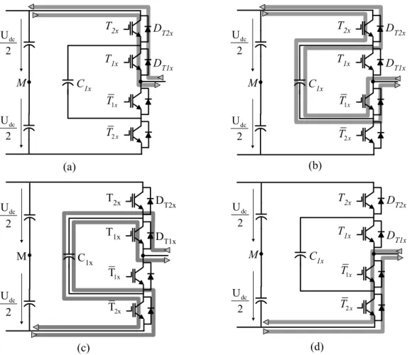
Figure 3-2 Switch states: (a) conduction paths, (b) commutations and switching losses of the 2L-VSC a b c [0 0 1] a b c [1 0 0] a b c [1 1 0] a b c [1 0 1] a b c [0 1 1] a b c [0 1 0] a b c [1 1 1] a b c [0 0 0] (a) DT1a T1a T2a a DT2a C2 C1 M -+ DT1a T1a T2a a DT2a C2 C1 M -+ 2 dc U 2 dc U 2 dc U 2 dc U (b) DT1a T1a T2a D T2a C2 C1 M -+ DT1a T1a T2a D T2a C2 C1 M -+ 2 dc U 2 dc U 2 dc U 2 dc U (c)
Table 3-1 Switch positions for each phase of the two-level VSC
The current paths for positive and negative phase currents iph are depicted in Figure 3-2b. In any switch state, one semiconductor lies within the current path. It should be noted that all
switches and diodes of the two-level VSC are stressed by Udc. Assuming a sinusoidal phase
current, the maximum switch/diode current is the maximum phase current ˆiph. These
parameters determine the rating of the main semiconductors.
Switching losses are created by the commutation processes between the different switch states. Only turn-on and turn-off losses of active switches and recovery losses of diodes are considered. Turn-on losses of diodes are usually small so that they can be neglected [1]. The distribution of the switching losses and the conduction losses are summarized in Table 3-2 and Table 3-3 respectively.
For a positive phase current iph > 0, the commutation (+ → –) is initiated by the turn-off of T1x and the current forced from T1x to DT2x(x = a, b, c). The situation is visualized in Figure 3-8c, where the current path of the switching active device is marked bold and the current path of the switching passive device is marked with a dashed line. The loss devices are encircled. In contrast, the commutation (– → +) is initiated by the turn-off of D2x and the current forced from DT2x to T1x.
For a negative phase current iph < 0, the commutation (+ → –) is initiated by the turn-off of DT1x and the current forced from DT1x to T2x. In contrast, the commutation (– → +) is initiated by the turn-off of T2x and the current forced from T2x to DT1x, as shown in Figure 3-8c.
Table 3-2 Conduction losses in the two-level VSC
Table 3-3 Switching losses in the two-level VSC
3.1.3.Sine-Triangle Modulation
The purpose of PWM three-phase converters is to shape and to control the three-phase output voltages in magnitude and frequency with an essentially constant input voltage Udc. To obtain balanced three-phase output voltages in a three-phase PWM, the same triangular voltage
State S1x S2x
Positive “+” (UxM = +Udc/2) 1 0
Negative “-” (UxM = -Udc/2) 0 1
State T1x T2x DT1x DT2x
Positive phase current “+” ×
“-” ×
Negative phase current
“+” ×
“-” ×
State T1x T2x DT1x DT2x
Positive phase current
+ ↔ − × ×
Negative phase current
![Figure 2-2 illustrates two examples of medium voltage drives: Figure 2-2a shows a medium voltage drive using an IGBT-based 3L-NPC inverter (SIMOVERT [9])](https://thumb-us.123doks.com/thumbv2/123dok_us/8692497.2351889/29.892.148.743.251.717/figure-illustrates-examples-voltage-figure-voltage-inverter-simovert.webp)