Correlation of energy disorder and open-circuit
voltage in hybrid perovskite solar cells
Yuchuan Shao, Yongbo Yuan and Jinsong Huang
*
Organometal trihalide perovskites have been demonstrated as excellent light absorbers for high-efficiency photovoltaic applications. Previous approaches to increasing the solar cell efficiency have focused on optimization of the grain morphology of perovskite thin films. Here, we show that the structural order of the electron transport layers also has a significant impact on solar cell performance. We demonstrate that the power conversion efficiency of CH3NH3PbI3planar heterojunction photovoltaic cells increases from 17.1 to 19.4% when the energy disorder in the fullerene electron transport layer is reduced by a simple solvent annealing process. The increase in efficiency is the result of the enhancement in open-circuit voltage from 1.04 to 1.13 V without sacrificing the short-circuit current and fill factor. These results shed light on the origin of open-circuit voltage in perovskite solar cells, and provide a path to further increase their efficiency.
O
rganometal trihalide perovskite materials have been attracting considerable research interests for solar cell applications1–9owing to their many intriguing optical andelectronic properties, such as very high absorption coefficient10,
high charge carrier mobility11,12, long carrier recombination
lifetime12 and unique defect physics13. Benefiting from these
excellent properties, the power conversion efficiency (PCE) of perovskite photovoltaic devices has been greatly improved from 3.8% (ref. 14) to a certified 20.1% (ref. 15) in less than five years of development. One origin of the high PCE of the perovskite solar cells is the relatively large ratio of the open-circuit voltage (VOC) to
bandgap (Eg)—approximately 0.69 (ref. 16). Compared to typical
excitonic organic solar cells with a ratio of about 0.55 VOC/Eg
(ref. 16), perovskite solar cells show a much lower photon energy loss. However, theirVOC/Egratio is still lower than the value of 0.80
for amorphous silicon and GaAs thin film solar cells16. Given that
first-order charge recombination rates in perovskite materials have been shown to be weak owing to the unusual defect physics13, there
is still considerable scope to further increase the PCE of perovskite solar cells by boostingVOC. This is even more urgent in the case
of planar heterojunction perovskite cells, which are very simple to fabricate using a low-temperature solution process, but usually have a lower maximum VOC than the ‘inverted’
mesoporous-structure devices15,17–19. In fact13, it has been demonstrated by
both simulation and experimental results that a large degree of energy disorder of the photoactive layer would cause a significant drop in the value of VOC for organic bulk heterojunction solar
cells20,21. In the past few years of perovskite device research,
most efforts have been focused on improving the crystallinity— or reducing the energy disorder—of the perovskite thin films. However, barely any attention has been paid to the organic charge transport materials, which inevitably introduce energy disorder into perovskite devices. The low carrier mobility of most organic charge transport materials, such as 2,20
,7,70
-tetrakis-(N,N di-p-methoxyphenylamine) 9,90
-spirobifluorene (spiro-OMeTAD)5,6,22,
phenyl-C61-butyric acid methyl ester (PCBM; refs 19,23,24) and poly[bis(4-phenyl)(2,4,6-trimethylphenyl)amine] (PTAA; refs 17,23), indicates they have a high degree of energy disorder. The importance of the energy level alignment of the charge
transport layers with perovskite on the VOC of perovskite solar
cells has been recognized recently, especially for large-bandgap perovskite solar cells23,25. Nevertheless, there are hardly any studies
on the influence of energy disorder in these charge transport layers on theVOCof perovskite solar cells. To maximize the opportunities
of perovskite materials for photovoltaics applications, it would be desirable to have a full understanding of the detrimental effects of energy disorder in components other than the perovskite layer, and to find strategies to mitigate the energy disorder in perovskite solar cells.
In this paper, we report the influence of energy disorder in fullerene electron transport layers on the VOC of planar
heterojunction perovskite solar cells. A simple solvent annealing method is found to mitigate the energy disorder by reducing material structural disorder, which enhances the VOC of the
CH3NH3PbI3 planar heterojunction device from 1.04 to 1.13 V
without decreasing the device short-circuit current (JSC) or fill factor
(FF). The results highlight the importance of reducing the energy disorder in the charge carrier transport layer.
Photovoltaic device structure and performance
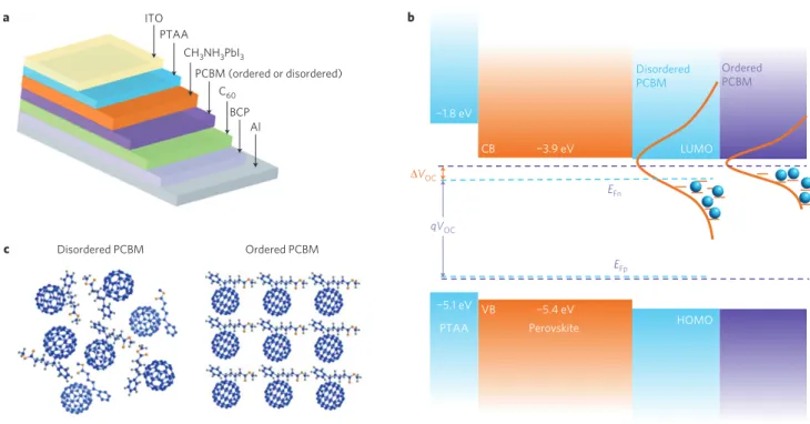
The planar heterojunction perovskite solar cells in this study were structured as ITO/PTAA/CH3NH3PbI3 (550–600 nm)/
PCBM(20 nm)/C60(20 nm)/BCP(8 nm)/Al(100 nm), as shown
in Fig. 1a, where ITO is indium tin oxide, BCP is 2,9-dimethyl-4,7-diphenyl-1,10-phenanthroline, and Al is aluminium. The MAPbI3
layers were formed by the interdiffusion of lead iodide (PbI2)
and a methyl ammonium iodide (CH3NH3I, CH3NH3 = MA)
stacking layer24, followed by a solvent annealing process10. It forms
smooth, compact perovskite films with an average grain size much larger than the thin film thickness26. Then the PCBM layer was
spun on top of the perovskite layer and thermally annealed at a temperature of 100◦
C for one hour with or without the presence of dichlorobenzene (DCB) vapour. The PCBM layer here acts not only as the electron transport layer, but also as a passivation layer to reduce the surface and grain boundary trap density of the perovskite grains18,27. The devices were then finished by thermally
evaporating C60 (20 nm), BCP (8 nm) and aluminium (100 nm)
layers in sequential order.
ITO PTAA
CH3NH3PbI3
PCBM (ordered or disordered) C60
BCP Al
Disordered PCBM Ordered PCBM
qVOC
EFn
EFp
CB
VB
Perovskite
Disordered PCBM
PTAA −5.1 eV −1.8 eV
−5.4 eV
−3.9 eV LUMO
HOMO
ΔVOC
Ordered PCBM
a b
c
Figure 1| Device structure and mechanism to enhanceVOCby reducing energy disorder.a, Device structure of the perovskite planar heterojunction solar
cells: ITO/PTAA/PCBM/C60/BCP/Al. Here ITO is indium tin oxide, PTAA is poly[bis(4-phenyl)(2,4,6-trimethylphenyl)amine], PCBM is
CH3NH3PbI3/phenyl-C61-butyric acid methyl ester, BCP is 2,9-dimethyl-4,7-diphenyl-1,10-phenanthroline and Al is aluminium.b, Schematic illustration of
how energy disorder of the PCBM layer influences the deviceVOC: a wide distributed DOS reduces the quasi-Fermi level of the photogenerated electrons
(EFn) and thus reduces the deviceVOC.EFpis the quasi-Fermi level of the photogenerated holes. Blue and purple dashed lines represent the quasi-Fermi
level of devices with disordered and ordered PCBM, respectively.c, Schematic of disordered and ordered PCBM structures formed by the solvent and thermal annealing processes.
Figure 1b illustrates the principle used to enhance theVOC of
the planar heterojunction perovskite devices by reducing the energy disorder in the electron transport layer. The electronic states of the organic PCBM thin films are subject to a large energy disorder originating from their structural and chemical disorder, such as low crystallinity and random molecular orientation, interactions with neighbouring molecules, impurities, and so on. Here we did not consider the energy disorder in the perovskite layer because, unlike the organic charge transport materials, the perovskite layer fabricated by the low-temperature solution process still has excellent crystallinity with a very low density of trap states and low energy disorder10. As a result, perovskite materials have relatively sharp
valence band (VB) and conduction band (CB) edges in the density-of-states diagram, which is consistent with the results of external quantum efficiency (EQE) measurements. TheVOCin a
photovoltaic device is determined by the quasi-Fermi level splitting of electrons and holes in the whole device under illumination, which is affected by the occupation of the available electronic states by photogenerated charge carriers, not only in the perovskite layer, but also in the charge transport layers. The band tail caused by the energy disorder of the PCBM layer that extends into the forbidden gap introduces additional electronic states. The non-equilibrium photogenerated electrons tend to relax down to these states when they travel through the PCBM layer, which results in reduced quasi-Fermi level splitting and a smallerVOC. From a carrier dynamics
point of view, the charge transit time through the PCBM layer is of the order of 100 ns, as calculated from its low mobility of 10−3cm2V−1s−1(ref. 28), which is much longer than the reported
electron relaxation time in the PCBM layer, which is of the order of
∼100 ps (ref. 29).
It is noted that the energy disorder of solid molecules depends strongly on the film preparation process as well as the intrinsic properties of the molecular structure. Therefore, our strategy is
to increase the crystallinity to mitigate the energy disorder of the PCBM layer, as illustrated in Fig. 1c, which narrows down the band tail electronic states and increases theVOCof the perovskite
solar cells. To realize this scenario, a 1,2-dichlorobenzene (DCB) vapour environment was introduced during the PCBM thermal annealing process. DCB gives very good solubility with respect to PCBM, but can barely dissolve the hybrid perovskites. The process is similar to solvent annealing in polymer bulk heterojunction solar cell fabrication30,31. Therefore, the DCB vapour treatment
can improve the crystallinity and decrease the energy disorder of the PCBM layer without damaging the perovskite layer. In this work, thermally annealed PCBM layers treated with and without DCB solvent vapour are referred to as ‘SA PCBM’ and ‘TA PCBM’, respectively.
Figure 2a shows the photocurrent curves of the optimized MAPbI3 devices with TA and SA PCBM, measured under one
simulated sun illumination. After decreasing the energy disorder of the PCBM, the device PCE increased from 17.1 to 19.4%. The increase in PCE here comes mainly from the enhancement inVOC
from 1.04 to 1.13 V, whereasJSCand FF remained∼22.6 mA cm
−2
and∼75.0%, respectively. The series resistances for devices with TA and SA PCBM are 5.15cm2and 3.80cm2, respectively, and the
shunt resistances for devices with TA and SA PCBM are 2,564cm2
and 2,380cm2, respectively. The photocurrents showed negligible
hysteresis (see Supplementary Fig. 1) as a result of the effective deactivation of surface and grain boundary charge traps by the double fullerene layers27. Figure 2b shows the EQE spectrum and
integrated JSC for the SA PCBM device. The integrated JSC of
22.3 mA cm−2is in good agreement with theJ
SCfromJ–Vscanning.
The steady-state measurements forVOC,JSC and PCE are shown
in Fig. 2c, which confirms the device performance parameters extracted from the photocurrent curves and verifies the absence of photocurrent hysteresis in our devices. The statistics of the
SA PCBM: VOC = 1.13 V PCE = 19.4%
TA PCBM:
VOC = 1.04 V
PCE = 17.1%
a
c
b
d
400 500 600 700 800
0 20 40 60 80 100
EQE (%)
Percentage (%)
Integrated
J
SC
(mA cm
−2
)
Wavelength (nm)
0 5 10 15 20 25
0.0 0.2 0.4 0.6 0.8 1.0 1.2
−25 −20 −15 −10 −5 0
Current density (mA cm
−2)
Voltage (V)
1.02 1.04 1.06 1.08 1.10 1.12 1.14 0
10 20 30 40 50
SA PCBM TA PCBM
VOC = 1.10 V VOC = 1.04 V
1.10 1.15 1.20
−23.5 −23.0 −22.5
0 50 100 150 200 250
18.5 19.0 19.5
Eff (%)
JSC
(mA cm
−2)
VOC
(V)
VOC (V) Time (s)
Figure 2| PCBM treatment-dependent device performance.a, Current density–voltage (J–V) characteristics of devices with solvent annealing (SA) and
thermal annealing (TA) PCBM layers.b, EQE and EQE-based integratedJSCof the devices with SA PCBM.c, Steady-state measurements ofVOC,JSCand
PCE for devices with SA PCBM.d, Statistics of theVOCdistribution for devices with TA PCBM (14 samples) and SA PCBM (16 samples). Blue and orange
solid lines represent the Gaussian distribution fitting for the statistics ofVOC.
VOCdistribution shown in Fig. 2d demonstrates the reliability and
repeatability of theVOCenhancement achieved by the
DCB-vapour-treatment-induced reduction of energy disorder in the PCBM layer.
Energy disorder characterization
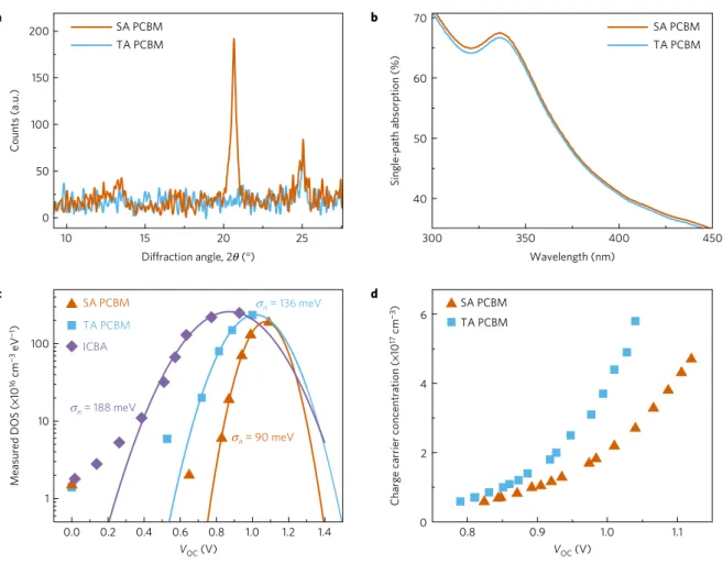
To verify that DCB vapour treatment can enhance the crystallinity of the PCBM, we performed X-ray diffraction (XRD) measurements of the spun PCBM films on glass substrates with and without DCB treatment. Figure 3a clearly shows a sharp diffraction peak at 20.5◦ appearing in the XRD spectrum of the SA PCBM thin film, whereas there is hardly any diffraction peak in the TA PCBM film, thus supporting the conclusion of enhanced crystallization in the SA PCBM (ref. 32). The absorption spectra of SA and TA PCBM were also measured. The slightly enhanced absorption also supports the better crystallinity in the ordered PCBM thin films. There is no obvious morphological difference between SA and TA PCBM on the perovskite layers, as shown in Supplementary Fig. 2.
We also directly characterized the energy disorder in the whole device by measuring the distribution of the electronic density of states (DOS) to confirm that the enhanced PCBM structure order can reduce energy disorder. The distribution of the density of states is often described by a Gaussian shape in organic semiconductors33.
gn(E−EL)=
Nn
√
2πσn exp
−(EL−E) 2
2σ2
n
(1)
whereNn is the total density per unit volume,EL is the energy
centre of the DOS, andσnis a disorder parameter that represents
the broadening of the DOS. Here we investigated the variation of the DOS distribution by extracting the chemical capacitance (Cµ) by means of impedance spectroscopy. It has been established that the chemical capacitance in this type of measurement is proportional to the DOS, asCµreflects the capability of a photovoltaic device to accept or release additional charge carriers as a result of shifts in the quasi-Fermi level34. When the quasi-Fermi level moves across
these electronic states, the release of occupied charge is recorded as a change in the chemical capacitance, thus providing a perfect tool to study the DOS distribution in the devices. The measurement details can be found in Supplementary Note 1. Fittings of the Gaussian DOS for perovskite solar cell devices with TA and SA PCBM films are shown in Fig. 3a. The experimental data were well fitted by equation (1) for all the devices measured. The disorder parameter σn decreased from 136 to 90 meV after replacing the TA PCBM with its SA counterpart. Because the perovskite layer is highly crystalline, the measured energy disorder should be dominated by the contribution from the PCBM layer, and the measured σn variation should reflect the degree of disorder in the PCBM layer resulting from the different PCBM treatments. The direct observation of reduced energy disorder in the device with SA PCBM fully supports our proposed scenario. A σn of 73 meV has been reported in pure PCBM devices according to disordered hopping transport models35. The relatively larger σ
n in our devices may originate from additional electronic interactions between PCBM and the perovskite layer, or from disorder contributions of the thermally evaporated C60 layer. We also measured the energy
b
d
0.0 0.2 0.4 0.6 0.8 1.0 1.2 1.4 1
10 100
SA PCBM
TA PCBM ICBA
0.8 0.9 1.0 1.1
0 2 4 6
300 350 400 450
40 50 60 70
Wavelength (nm)
SA PCBM TA PCBM
a
c
10 15 20 25
0 50 100 150 200
Diffraction angle, 2 (θ °) SA PCBM
TA PCBM
Counts (a.u.)
Measured DOS (
×
10
16 cm −3 eV −1)
Single-path absorption (%)
Charge carrier concentration (
×
10
17 cm −3)
VOC (V) VOC (V)
SA PCBM TA PCBM
n = 188 meV
σ
n = 136 meV
σ
n = 90 meV
σ
Figure 3| Structure and energy disorder of PCBM films under different treatments.a, XRD patterns of SA and TA PCBM thin films.b, Single-path
absorption of SA and TA PCBM thin films.c, Measured DOS of devices with SA PCBM, TA PCBM and ICBA extracted from their impedance spectra. The disorder parameterσnis obtained by fitting the DOS curves with a Gaussian distribution.d, Charge density generated in the device with SA and TA PCBM layers measured by the TPV and TPC method.
1 10 100
1 10
Light intensity (mW cm−2) a
1016 1017 1018
1 10
Charge carrier density (cm−3)
Lif
etime (
µ
s)
b
Lif
etime (
µ
s)
SA PCBM TA PCBM
SA PCBM TA PCBM
Figure 4| Dependence of charge recombination lifetime on PCBM treatment.a,b, Charge recombination lifetime in devices with SA and TA PCBM layers
measured by the TPV transient photovoltaic method as a function of bias light intensity (a) and charge carrier density (b).
(ICBA) layer, which is widely applied in organic solar cells to yield a largerVOC, because ICBA has a higher lowest unoccupied molecular
orbital (LUMO) level than that of PCBM. Replacing PCBM by ICBA indeed increased theVOCof the perovskite/fullerene hybrid
Schottky junction devices19. In those devices, the perovskite layers
were not continuous, and the direct contact of fullerenes with the hole transport layer formed a Schottky junction19. However, a
lower PCE of 12.8% andVOCof 0.97 V were obtained using ICBA
(Supplementary Fig. 3), similar to previous results (ref. 36). The unexpected results could be explained as due to the much larger energy disorder of the ICBA layer than the PCBM layers, which eventually reduces the quasi-Fermi energy of the electrons in ICBA. Another method to study the influence of energy disorder on VOC is to measure the density of photogenerated charges
0.0 0.2 0.4 0.6 0.8 1.0 1.2 −25
−20 −15 −10 −5 0
20 nm PCBM SA TA
30 nm PCBM SA TA
60 nm PCBM SA TA
Current density (mA cm
−2)
Voltage (V)
0.95 1.00 1.05 1.10 1.15 1.20
20 30 40 50 60
0.4 0.5 0.6 0.7
TA PCBM
SA PCBM
TA PCBM
VOC
(V)
Fill factor
SA PCBM
PCBM thickness (nm)
b a
Figure 5| Dependence of device performance on PCBM thickness.a, Current density–voltage (J–V) characteristics of devices with different thicknesses
(20, 30 and 60 nm) and different treatments (SA and TA) for the PCBM layer.b, Dependence of the open-circuit voltage and fill factor on the TA and SA PCBM thickness as extracted from theJ–Vcurves ina.
that is needed to produce a given quasi-Fermi level splitting. A method combining transient photovoltage spectroscopy (TPV) and transient photocurrent spectroscopy (TPC) was established to determine the generated carrier concentration before recombination20. This is also enabled by the much longer carrier
recombination lifetime demonstrated in hybrid perovskite materials than the charge extraction time out of the device26,27. Details of
the measurement techniques in the TPV and TPC methods are given in Supplementary Note 2. The results in Fig. 3d clearly show that a larger carrier concentration of carriers is needed to fill the low-energy levels in the device with TA PCBM to reach the same VOC as the device with SA PCBM, indicating the effectiveness of
our solvent annealing method for energy disorder mitigation. In addition, at the same generated charge density of 3×1017cm−3,
for instance, the devices with TA and SA PCBM haveVOCvalues
of 0.99 V and 1.07 V, respectively. This result is also consistent with our scenario that the same charge generation density (or light intensity) could generate a higherVOCin the devices with mitigated
energy disorder.
Besides the degree of energy disorder, charge carrier recombination dynamics in a solar cell can also impact the deviceVOC, because changes in the charge carrier recombination
rate would cause variations of the equilibrium charge carrier concentration, the quasi-Fermi level splitting, and thus the VOC
in the photovoltaic devices. However, in our study, the VOC
enhancement is not related to changes in the charge recombination dynamics, because no evidence of a change in the recombination lifetime was found in the TPV measurements, as shown in Fig. 4a,b. The charge recombination lifetimes for devices with SA and TA PCBM are the same under any given illumination light intensity and charge carrier density. A simulation also supports the scenario, as shown in Supplementary Note 3. Furthermore, the unchanged recombination rate reveals that the deeper electronic states induced by the energy disorder of TA PCBM do not act as recombination centres. Although the photogenerated electrons relax to the lower energy states, electrons are not trapped there which would otherwise cause reducedJSCand FF in devices with different PCBM
treatments. The ‘cooled’ electrons in the lower energy states can still efficiently transport out of PCBM layer by hopping to the cathode. Therefore, these lower energy electron states do not act as ‘traps’ and have negligible influence on the charge extraction efficiency.
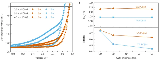
Dependence of device performance on PCBM thickness Finally, the dependence of the device performance on PCBM thickness was examined, as shown in Fig. 5a,b. The thickness of the
TA and SA PCBM layer was varied from 20 to 60 nm by tuning the concentration of the PCBM solution and the spin-coating rate. The VOCvalues of all the devices with SA PCBM are higher than those
of the devices with TA PCBM, regardless of the PCBM thickness, which demonstrates the effectiveness of the reduced energy disorder in enhancing the device VOC. As the PCBM thickness increases,
theVOC values of devices with both SA and TA PCBM remain
almost invariant, whereas the FF is reduced markedly. The different trends in the variations of VOC and FF reflect that the change
of series resistance of the electron transport layer, which was in accordance with the expectation for the PCBM thickness increase, now impact only the deviceVOC. Thus, a thin electron transport
layer is beneficial in reducing the series resistance and improving the charge extraction and device performance, which is of importance for PCBM, given its relatively low mobility.
Conclusion
We have revealed and highlighted the importance of energy disorder mitigation in electron transport layers as a means to improve the VOCin perovskite solar cells. Enhanced PCBM structural ordering
effectively reduces the energy disorder, as can be deduced from the significant decrease in the DOS and disorder parameters. A recent independent theoretical work investigating energy disorder in fullerenes has reported the same disorder parameter for ordered and disordered PCBM, and shown excellent agreement with our experimental results37. This technique presents an effective
method to increaseVOCwithout sacrificing eitherJSC or FF. Most
importantly, a new direction has been indicated towards further increasing the PCE of perovskite solar cells by the design and application of new electron transport materials with even smaller energy disorder than SA PCBM. We speculate that a reduction in the energy disorder for the hole transport layer would also have an impact on theVOCof perovskite solar cells. In addition, selecting
charge transport materials carefully and optimizing the interfaces between the perovskite layer and the charge transport layers could potentially decrease the interfacial energy disorder and obtain a larger open-circuit voltage.
Methods
Device fabrication.The hole transport layer, PTAA film was prepared by spin-coating 0.5 wt% PTAA solution at 6,000 r.p.m. The as-prepared film was then thermally annealed at 110◦
C for 10 min. The MAPbI3films were fabricated by the solvent annealing induced interdiffusion method27. The film fabrication procedures are the same as previous studies, whereas the PbI2layer on PTAA should be spin-coated from a 100◦
a 75 mg ml−1methylammonium iodide (MAI) 2-propanol precursor solution. After they were cooled down to room temperature, PCBM (dissolved into dichlorobenzene (DCB), 2 wt%) was spun on top of the formed perovskite layers. After that, for PCBM treated with solvent annealing, the devices were put on top of a hot plate and covered by a glass Petri dish. 10µl of DCB solvent was added at the edge of the Petri dish during the thermal annealing process, so that the DCB vapour could go into the Petri dish and make contact with the PCBM layer. For control devices with just thermal annealing PCBM, no DCB solvent was added during the thermal annealing process. The devices were finished by thermally evaporating C60(20 nm), BCP (8 nm) and aluminium (100 nm) in sequential order. The device working area was 8 mm2, as defined by the overlap of the ITO substrate and the Al cathode.
Device characterization.Simulated AM 1.5 G irradiation (100 mW cm−2) was produced by a Xenon-lamp-based solar simulator (Oriel 67005, 150 W Solar Simulator) for current (I)–voltage (V) measurements. The light intensity was calibrated by a silicon (Si) diode (Hamamatsu S1133) equipped with a Schott visible colour glass filter (KG5 colour filter). A Keithley 2400 Sourcemeter was used for theI–Vmeasurements. The scanning rate was 0.1 V s−1. The steady-state VOCandJSCwere measured by zero-bias current and zero-bias voltage versus time, respectively. The steady-state PCE was measured by monitoring the current with a 0.91 V bias voltage. XRD measurements were performed with a Rigaku D/Max-B X-ray diffractometer in the Bragg–Brentano parafocusing geometry, a diffracted-beam monochromator, and a conventional cobalt target X-ray tube set to 40 kV and 30 mA. The single-path absorption was measured using an Evolution 201 ultraviolet–visible spectrometer (Thermo Scientific).
Received 17 August 2015; accepted 20 October 2015; published 11 January 2016
References
1. Green, M. A., Ho-Baillie, A. & Snaith, H. J. The emergence of perovskite solar cells.Nature Photon.8, 506–514 (2014).
2. Snaith, H. J. Perovskites: The emergence of a new era for low-cost, high-efficiency solar cells.J. Phys. Chem. Lett.4, 3623–3630 (2013). 3. Dong, Q.et al.Electron–hole diffusion lengths>175µm in solution-grown
CH3NH3PbI3single crystals.Science347, 967–970 (2015).
4. Xing, G.et al.Low-temperature solution-processed wavelength-tunable perovskites for lasing.Nature Mater.13, 476–480 (2014).
5. Liu, M., Johnston, M. B. & Snaith, H. J. Efficient planar heterojunction perovskite solar cells by vapour deposition.Nature501, 395–398 (2013). 6. Lee, M. M., Teuscher, J., Miyasaka, T., Murakami, T. N. & Snaith, H. J. Efficient
hybrid solar cells based on meso-superstructured organometal halide perovskites.Science338, 643–647 (2012).
7. Abrusci, A.et al.High-performance perovskite-polymer hybrid solar cells via electronic coupling with fullerene monolayers.Nano Lett. 13, 3124–3128 (2013).
8. Stranks, S. D.et al.Electron–hole diffusion lengths exceeding 1 micrometer in an organometal trihalide perovskite absorber.Science342, 341–344 (2013). 9. Heo, J. H.et al.Efficient inorganic–organic hybrid heterojunction solar cells
containing perovskite compound and polymeric hole conductors.Nature Photon.7, 486–491 (2013).
10. Xiao, Z.et al.Solvent annealing of perovskite-induced crystal growth for photovoltaic-device efficiency enhancement.Adv. Mater.26, 6503–6509 (2014). 11. Takahashi, Y., Hasegawa, H., Takahashi, Y. & Inabe, T. Hall mobility in tin
iodide perovskite CH3NH3SnI3: Evidence for a doped semiconductor.J. Solid State Chem.205, 39–43 (2013).
12. Wehrenfennig, C., Eperon, G. E., Johnston, M. B., Snaith, H. J. & Herz, L. M. High charge carrier mobilities and lifetimes in organolead trihalide perovskites. Adv. Mater.26, 1584–1589 (2014).
13. Yin, W.-J., Shi, T. & Yan, Y. Unusual defect physics in CH3NH3PbI3perovskite solar cell absorber.Appl. Phys. Lett.104, 063903 (2014).
14. Kojima, A., Teshima, K., Shirai, Y. & Miyasaka, T. Organometal halide perovskites as visible-light sensitizers for photovoltaic cells.J. Am. Chem. Soc. 131, 6050–6051 (2009).
15. Jeon, N. J.et al.Compositional engineering of perovskite materials for high-performance solar cells.Nature517, 476–480 (2015).
16. Green, M. A., Emery, K., Hishikawa, Y., Warta, W. & Dunlop, E. D. Solar cell efficiency tables (Version 45).Prog. Photovolt. Res. Appl.23, 1–9 (2015). 17. Jeon, N. J.et al.Solvent engineering for high-performance inorganic–organic
hybrid perovskite solar cells.Nature Mater.13, 897–903 (2014).
18. Xu, J.et al.Perovskite–fullerene hybrid materials suppress hysteresis in planar diodes.Nature Commun.6, 7081 (2015).
19. Wang, Q.et al.Large fill-factor bilayer iodine perovskite solar cells fabricated by a low-temperature solution-process.Energy Environ. Sci. 7, 2359–2365 (2014).
20. Heumueller, T.et al.Disorder-induced open-circuit voltage losses in organic solar cells during photoinduced burn-in.Adv. Energy Mater.5, 1500111 (2015). 21. Blakesley, J. C. & Neher, D. Relationship between energetic disorder and
open-circuit voltage in bulk heterojunction organic solar cells.Phys. Rev. B84, 075210 (2011).
22. Liu, D. & Kelly, T. L. Perovskite solar cells with a planar heterojunction structure prepared using room-temperature solution processing techniques. Nature Photon.8, 133–138 (2014).
23. Ryu, S.et al.Voltage output of efficient perovskite solar cells with high open-circuit voltage and fill factor.Energy Environ. Sci.7, 2614–2618 (2014). 24. Xiao, Z.et al.Efficient, high yield perovskite photovoltaic devices grown by
interdiffusion of solution-processed precursor stacking layers.Energy Environ. Sci.7, 2619–2623 (2014).
25. Zhou, H.et al.Interface engineering of highly efficient perovskite solar cells. Science345, 542–546 (2014).
26. Bi, C.et al.Non-wetting surface-driven high-aspect-ratio crystalline grain growth for efficient hybrid perovskite solar cells.Nature Commun. 6, 7747 (2015).
27. Shao, Y., Xiao, Z., Bi, C., Yuan, Y. & Huang, J. Origin and elimination of photocurrent hysteresis by fullerene passivation in CH3NH3PbI3planar heterojunction solar cells.Nature Commun.5, 5784 (2014).
28. Von Hauff, E., Dyakonov, V. & Parisi, J. Study of field effect mobility in PCBM films and P3HT: PCBM blends.Sol. Energy Mater. Sol. Cells87, 149–156 (2005). 29. Xie, Y.et al.Femtosecond time-resolved fluorescence study of P3HT/PCBM
blend films.J. Phys. Chem. C114, 14590–14600 (2010).
30. Li, G.et al.‘‘Solvent annealing’’ effect in polymer solar cells based on poly (3-hexylthiophene) and methanofullerenes.Adv. Funct. Mater. 17, 1636–1644 (2007).
31. Li, G.et al.High-efficiency solution processable polymer photovoltaic cells by self-organization of polymer blends.Nature Mater.4, 864–868 (2005). 32. Mens, R.et al.Description of the nanostructured morphology of
[6, 6]-phenyl-C61-butyric acid methyl ester (PCBM) by XRD, DSC and solid-state NMR.Magn. Reson. Chem.49, 242–247 (2011).
33. Bisquert, J. Interpretation of electron diffusion coefficient in organic and inorganic semiconductors with broad distributions of states.Phys. Chem. Chem. Phys.10, 3175–3194 (2008).
34. Pomerantz, Z.et al.Capacitance, spectroelectrochemistry and conductivity of polarons and bipolarons in a polydicarbazole based conducting polymer. J. Electroanal. Chem.614, 49–60 (2008).
35. Mihailetchi, V. D.et al.Electron transport in a methanofullerene.Adv. Funct. Mater.13, 43–46 (2003).
36. Hu, M.et al.Distinct exciton dissociation behavior of organolead trihalide perovskite and excitonic semiconductors studied in the same system.Small11, 2164–2169 (2015).
37. Tummala, N. R., Zheng, Z., Aziz, S. G., Coropceanu, V. & Brédas, J.-L. Static and dynamic energetic disorders in the C60, PC61BM, C70, and PC71BM fullerenes.J. Phys. Chem. Lett.6, 3657–3662 (2015).
Acknowledgements
The authors gratefully acknowledge financial support from the National Science Foundation (DMR-1505535), the Department of Energy (DE-EE0006709) and the Office of Naval Research (N00014-15-1-2713).
Author contributions
J.H. and Y.S. conceived the idea, designed the experiments and wrote the paper. Y.Y. conducted the X-ray diffraction measurements and Y.S. carried out all other experiments. J.H. supervised the project.
Additional information
Supplementary information is availableonline. Reprints and permissions information is
available online atwww.nature.com/reprints. Correspondence and requests for materials
should be addressed to J.H.
Competing interests
The authors declare no competing financial interests.