CHARGE TRANSPORT IN ORGANIC AND ORGANOMETALLIC MOLECULES:DEVICE DESIGN,
FABRICATION, AND TESTING
Robert Charles Bruce
A dissertation submitted to the faculty at the University of North Carolina at Chapel Hill in partial fulfillment of the requirements for the degree of Doctor of Philosophy in the Department
of Chemistry.
Chapel Hill 2015
Approved by: Wei You
ii
iii
ABSTRACT
Robert Charles Bruce: Charge Transport in Organic and Organometallic Molecules: Device Design, Fabrication, and Testing
(Under the direction of Wei You)
Molecular electronics (ME) represents a frontier for electronics. Designing electronic devices at the single molecule level would lead to extremely high density devices, and the organic materials typically used in ME can bring switchable properties and enable formation of transistors at the single molecule level. While promising, potential issues arise from
incorporating these organic-based materials and their unique properties into electronic devices. Solutions exist to generate electrical devices with organic materials, but understanding the impacts of these fabrication processes is necessary for their use in practical application settings.
The focus of this work is studying unique organic and organometallic materials in molecular electronic device architectures designed toward use in practical electronic settings. Spin-active organometallic complexes – a cobalt bis(dioxylene) based valence tautomer (CoVT), and multi[(porphinato)metal] oligomer wires – are used to build molecular wires and studied in ME settings designed through self-assembly approaches. While the CoVT molecule is shown to actually lose its valence tautomerism when tethered to a surface, the porphyrin wires show metal center dependence on charge transport properties, enabling them to be used in potentially
switchable ME and spintronic devices.
iv
other electrically identical architectures. We explain the force effects from nTP to be a possible cause and use this as a case study in highlighting the impact architecture can have on monolayer properties. Despite this, porphyrin wires in nTP junctions exhibit near identical electrical
properties compared to single molecule measurements, highlighting the technique’s ability to exhibit the electrical properties of more specialized and complex molecules.
Other soft lithographic techniques were also highlighted toward designing
v
Dedicated to all the teachers that helped me grow and pushed me,
vi
ACKNOWLEDGEMENTS
First, I need to thank my advisor, Wei You. Wei, I’m so appreciative for letting me be a part of your group. You gave me every opportunity to succeed, let me learn and work on so many diverse things, and opened any door that needed it. I don’t know if I’ll ever meet a professor who cared so much about his students. Thank you so much.
I’d also like to thank my amazing sub-groupmates, Travis, Josh, Jeremy, and Elizabeth. The past five years have been an amazing experience, and I can’t imagine asking for better people to work with and learn from. I don’t think being a part of or simply watching random arguments will ever be so much fun. I’d be remiss if I left out a thanks for the rest of the You group as well, thank you for all of the research talks, BBQs, and board game nights. I’m sorry if I drove you guys nuts with XPS talks, but I hope something positive rubbed off of my nerdy obsessions.
There are so many other people that I could probably write a whole thesis-length document thanking, I hope it suffices for me to say thank you to the amazing people that have supported me over the past five years – my fellow classmates, the young adult group (and others) from UPC, choir members, and so many other people. It’s been a blessing to get to know you all and experience Chapel Hill with you; you are an inseparable part of the work in this thesis.
vii
TABLE OF CONTENTS
LIST OF FIGURES ...xiv
LIST OF TABLES ... xx
LIST OF EQUATIONS...xxi
LIST OF ABBREVIATIONS AND SYMBOLS ... xxii
CHAPTER 1: Introduction to Molecular Electronics and Spintronics ...1
1.1 Background ...1
1.2 Organic Materials for Electronic Applications ...4
1.2.1 Recent Interests in Organic Electronics ...4
1.2.2 Properties of Organics for Electronic Applications ...6
1.3 Molecular Electronics ...9
1.3.1 Synthetic Control of Molecular Electronic Properties ...9
1.3.2 Switchable Properties in Molecular Electronics ... 11
1.4 Organic Spintronics ... 12
1.4.1 Basics of Spintronics- Spin Valve ... 13
1.4.2 Basics of Organic Spintronics ... 16
1.4.3 Organic Magnetoresistance ... 16
viii
1.4.5 Interface Considerations in Organic Spintronics ... 21
1.4.6 Spintronics from Controlling Spin State in Organic-Based Molecules ... 24
1.5 Designing Devices with Organic-Based Materials ... 26
1.5.1 Techniques for Designing Molecular Electronic Devices ... 27
1.5.2 Soft Lithography and Transfer Printing in Molecular Electronics ... 29
1.6 Research Overview ... 30
1.7 References ... 32
CHAPTER 2: Adapting Spintronic Organometallic Molecules to Molecular Electronic Settings ... 38
2.1 Background ... 38
2.1.1 History of Magnetism in Metals ... 38
2.1.2 Magnetic Properties in Organic Molecules ... 43
2.2 Study of Iron Spin Crossover Films ... 45
2.2.1 Spin Crossover ... 45
2.2.2 Experimental- FeSCO Film Growth and Study ... 48
2.2.3 Results and Discussion- FeSCO ... 49
2.3 Study of Valence Tautomers Designed as Molecular Wires ... 52
2.3.1 Valence Tautomerism for Spintronic Devices ... 52
2.3.2 Experimental- CoVT Wire Growth and Study ... 57
ix
2.4 Conclusions... 70
2.5 Appendix ... 72
2.5.1 XPS Spectra for Various CoVT Wire Components ... 72
2.6 References ... 79
CHAPTER 3: Studying Phenylenedithiol Monolayers in Nanotransfer Printed Molecular Junctions ... 82
3.1 Background ... 82
3.1.1 Electrical Characterization of Molecular Junctions ... 82
3.1.2 Nanotransfer Printing ... 85
3.1.3 Alkanethiols in Nanotransfer Printed Junctions ... 86
3.1.4 Phenylenedithiol Self-Assembled Monolayers... 89
3.1.5 Overview ... 91
3.2 Experimental ... 92
3.2.1 Materials ... 92
3.2.2 Gold Substrate and Self-Assembled Monolayer Preparation ... 92
3.2.3 Nanotransfer Printing ... 93
3.2.4 Atomic Force Microscopy ... 93
3.2.5 X-Ray Photoelectron Spectroscopy ... 94
3.3 Results and Discussion ... 94
x
3.3.2 Phenylenedithiol Monolayer Characterization ... 100
3.3.3 nTP Characterization of Phenylenedithiol Monolayers ... 104
3.3.4 Influence of Device Architecture on Measured ME Properties... 109
3.4 Conclusions... 112
3.5 Appendix ... 114
3.5.1 Synthetic Procedures ... 114
3.5.2 NMR Spectra for Synthesized Compounds ... 117
3.6 References ... 121
CHAPTER 4: Studies of Multi[(Porphinato)Metal] Oligomer Wires in Molecular Electronic Devices ... 124
4.1 Background ... 124
4.1.1 Organic Heterocycles for Spintronic Effects ... 124
4.1.2 Spintronic Effects from Porphyrin Metal Centers ... 126
4.1.3 Molecular Electronic Studies of Porphyrin Wires ... 128
4.1.4 Overview ... 129
4.2 Methods ... 129
4.2.1 Materials ... 129
4.2.2 Gold Substrate and Self-Assembled Monolayer Preparation ... 130
4.2.3 Nanotransfer Printing ... 130
xi
4.2.5 Photoelectron Spectroscopy ... 131
4.2.6 Cyclic Voltammetry ... 132
4.3 Results and Discussion ... 132
4.3.1 Carbodithioate Linkers in Porphyrin Monolayers ... 132
4.3.2 Deprotection Effects on Metal Binding Groups ... 138
4.3.3 Thioacetyl Linkers in Porphyrin Monolayers ... 143
4.3.4 Picturing Porphyrin Wires on a Surface ... 145
4.3.5 Changing Porphyrin Metal Centers... 150
4.3.6 Nanotransfer Printed Porphyrin Oligomer Wire Devices ... 154
4.3.7 UPS Measurements of Porphyrin Monolayers ... 160
4.4 Conclusions... 166
4.5 Appendix ... 168
4.5.1 Synthetic Schemes ... 168
4.5.2 XPS Spectra ... 175
4.5.3 UPS Spectra ... 189
4.6 References ... 192
CHAPTER 5: Large Area Junctions from Soft Lithography for Macroscopically Accessible Molecular Electronic Devices ... 195
5.1 Background ... 195
xii
5.1.2 Overview ... 196
5.2 Methods ... 197
5.2.1 General ... 197
5.2.2 Atomic Force Microscopy ... 197
5.2.3 Kinetic Controlled Transfer Printing (KTP) ... 198
5.2.4 Electron Beam Lithography... 198
5.2.5 Oxygen Plasma Cleaning ... 199
5.2.6 Graphene Transfer and Device Fabrication ... 199
5.2.7 Raman Spectroscopy ... 200
5.2.8 PEDOT:PSS Devices ... 200
5.3 Results and Discussion ... 200
5.3.1 Nanoindentation of 200 nm nTP Features ... 200
5.3.2 Kinetic Controlled Transfer Printing ... 203
5.3.3 Graphene as a Molecular Electronic Buffer Layer ... 214
5.3.4 Evaluation of Macroscopic Fabrication Techniques ... 220
5.4 Conclusions... 224
5.5 Appendix ... 227
5.6 References ... 228
CHAPTER 6: Summary of Conclusions and Recommendations for Future Work ... 230
xiii
6.1.1 Adapting Spintronic Molecules to Molecular Electronic Settings ... 231
6.1.2 Studying Phenylenedithiol Monolayers in nTP Molecular Junctions ... 232
6.1.3 Studies of Porphyrin Oligomer Wires in Molecular Electronic Devices ... 233
6.1.4 Large Area Junctions from Soft Lithography for Macroscopic ME Junctions ... 234
6.2 Recommendations for Future Work ... 237
6.2.1 Thermally Stable Metal Binding Groups ... 237
6.2.2 Silicon Substrates for Analyzing Monolayer Properties ... 238
6.2.3 Solvent Assisted Transfer Printing ... 239
6.2.4 Metal Effects in Porphyrin Nanowires ... 242
6.3 Methods ... 244
6.3.1 Solvent Assisted Transfer Printing ... 244
xiv
LIST OF FIGURES
Figure 1.1 – Moore’s Law ...3
Figure 1.2 – Amdahl’s Law ...3
Figure 1.3 – Champion Solar Cell Efficiencies Based on Solar Cell Type...5
Figure 1.4 – Solution Processible Techniques for Large Scale OPV Production. ...6
Figure 1.5 – Examples of Post-Synthesis Switchable Properties in Organic Systems...8
Figure 1.6 – Altering Charge Transport Mechanisms in Molecular Wires ... 10
Figure 1.7 – Conductance Switching in Molecular Wires ... 11
Figure 1.8 – Spin Valve ... 13
Figure 1.9 – Organic Magnetoresistance (OMAR) in PEDOT/C60/Al devices ... 17
Figure 1.10 – Coulomb Blockade ... 18
Figure 1.11 – Organic Radicals for Spin Polarized Transport ... 20
Figure 1.12 – Engineering Spintronic Effects at Zinc Methyl Phenalenyl (ZMP) Interfaces ... 23
Figure 1.13 – Organic Magnetic Effects ... 25
Figure 1.14 – Molecular Electronic Junctions ... 27
Figure 1.15 – Molecular Electronics Devices Prepared with Buffer Layers. ... 28
Figure 2.1 – Magnetism in Manganese-Doped Carbon Nanotubes (CNTs) ... 42
Figure 2.2 – Levitating Frog in a 20 Tesla Magnet ... 43
Figure 2.3 – Possible Electron Configurations for d-shell in Fe2+ Complex... 46
Figure 2.4 – SQUID Magnetometry of Powder FeSCO ... 49
Figure 2.5 – FeSCO Color Change as a Function of Temperature ... 50
xv
Figure 2.7 – Cobalt bis(dioxylene) Molecule [CoVT] and its Valence Tautomer
Transition ... 54
Figure 2.8 – Effects on Valence Tautomerism from Different Ligands ... 56
Figure 2.9 – Attaching CoVT to a Surface ... 57
Figure 2.10 – CoVT Ligand Test on a Surface ... 59
Figure 2.11 – XPS Characterization of CoVT on a Surface... 60
Figure 2.12 – Steric Hindrance in CoVT Wires ... 63
Figure 2.13 – Polymerization of CoVT and Linker Group ... 64
Figure 2.14 – Cross Sectional AFM of CoVT Multilayers on Gold ... 66
Figure 2.15 – CoVT Monomer Wires at Variable Temperature ... 68
Figure 2.16 – CoVT Crystals on Au/SiOx Substrates ... 69
Figure 2.17 – Pyridine-dodecane-thiol Seed Monolayer XPS Spectra ... 72
Figure 2.18 – CNCoVT XPS Spectra ... 73
Figure 2.19 – CNCoVT/ bipy XPS Spectra... 74
Figure 2.20 – CNCoVT/ bipy/ CNCoVT XPS Spectra... 75
Figure 2.21 – CNCoVT/ DipyE XPS Spectra ... 76
Figure 2.22 – BrCoVT (110K) XPS Spectra ... 77
Figure 2.23 – BrCoVT (210K) XPS Spectra ... 78
Figure 3.1 – Nanotransfer Printing ... 86
Figure 3.2 – Octanethiol Self-Assembled Monolayer on Gold ... 87
Figure 3.3 – Alkanedithiol Monolayers Measured in Nanotransfer Printed Junctions ... 88
Figure 3.4 – Phenylenedithiol Calculated Rotation Energy ... 89
xvi
Figure 3.6 – qphDSH Monolayer Quality Based on TBAF Conditions ... 96
Figure 3.7 – Proposed Kinetics of ETMS Protection and Effects of Deprotectant Concentration ... 99
Figure 3.8 – XPS Spectra for Phenylenedithiol Monolayers ... 101
Figure 3.9 – Nanotransfer Printed Junctions with Phenylenedithiols ... 104
Figure 3.10 – Deprotected DS-ETMS Electrical Properties ... 105
Figure 3.11 – Phenylenedithiol nTP Characterization ... 106
Figure 3.12 – Electrical Measurements for Oligo-para-phenylenedithiol Devices... 108
Figure 3.13 – Synthetic Route for ETMS-protected Phenylenedithiols ... 114
Figure 3.14 – H-NMR for Synthesized qphD-SETMS ... 117
Figure 3.15 – 13C-NMR for Synthesized qphD-SETMS... 118
Figure 3.16 – H-NMR for Synthesized tphD-SETMS ... 119
Figure 3.17 – 13C-NMR for Synthesized tphD-SETMS ... 120
Figure 4.1 – Zinc Porphyrin Wires in STM-Break Junction ... 128
Figure 4.2 – PZn-CS2 Structure ... 132
Figure 4.3 – PZn1-CS2 Monolayers on Gold Substrates ... 135
Figure 4.4 – PZn1-CS2 Concentration Dependence ... 137
Figure 4.5 – XPS of Alkanecarbodithioate Monolayer ... 138
Figure 4.6 – XPS of Benzenecarbodithioate with ETMS Protection ... 140
Figure 4.7 – XPS of Benzenecarbodithioate Without Protection Group ... 141
Figure 4.8 – Phenylthioacetate Monolayers on Gold ... 142
Figure 4.9 – PZn-SAc Monolayers Prepared on Gold ... 144
Figure 4.10 – DFT Calculated Orientation for PZn1-CS2 ... 146
xvii
Figure 4.12 – PZn1-SAc Nanotransfer Printed Electrodes ... 150
Figure 4.13 – XPS of Metal Centers for Different PM1-SAc Species ... 151
Figure 4.14 – AFM of nTP Pads on PCu3-SAc from Different Solvents... 152
Figure 4.15 – Copper and Nickel Porphyrin Monomer Monolayers ... 153
Figure 4.16 – nTP Junction with PMn-SAc Monolayer ... 154
Figure 4.17 – Measured Electrical Devices for PZn-SAc Series ... 156
Figure 4.18 – Histograms for PM1-SAc nTP Junctions ... 157
Figure 4.19 – Length Dependent Resistance for PMn-SAc Junctions ... 158
Figure 4.20 – Cyclic Voltammetry Data for Porphyrin Wires ... 160
Figure 4.21 – UPS of Porphyrin Monomers ... 161
Figure 4.22 – Multibarrier Model for Molecules with Metal Binding Groups ... 164
Figure 4.24 – XPS- PZn1CS2- 0.1 mM, 1:4 PZn:TBAF ... 175
Figure 4.25 – XPS- PZn1CS2- 1 mM ... 176
Figure 4.26 – XPS- PZn1CS2- 10 mM ... 176
Figure 4.27 – XPS- PZn1CS2- 1:2 molecule: TBAF ... 177
Figure 4.28 – XPS- PZn1CS2- 1:4 molecule: TBAF ... 177
Figure 4.29 – XPS- PZn1CS2- 1:16 molecule: TBAF ... 178
Figure 4.30 – XPS- PZn1CS2- Excess TBAF ... 178
Figure 4.31 – XPS- C10CS2 ... 179
Figure 4.32 – XPS- PhCS2-ETMS- 1:2 molecule: TBAF ... 179
Figure 4.33 – XPS- PhCS2-ETMS- 1:8 molecule: TBAF ... 180
Figure 4.34 – XPS- PhCS2-ETMS- Excess TBAF ... 180
xviii
Figure 4.36 – XPS- PhCS2-H- With TBAF ... 181
Figure 4.37 – XPS- PhSAc- 1 mM ... 182
Figure 4.38 – XPS- PZn1-SAc ... 183
Figure 4.39 – XPS- PZn2-SAc ... 183
Figure 4.40 – XPS- PZn3-SAc ... 184
Figure 4.41 – XPS- PCu1-SAc DCM ... 184
Figure 4.42 – XPS- PCu2-SAc DCM ... 185
Figure 4.43 – XPS- PCu3-SAc DCM ... 186
Figure 4.44 – XPS- PNi1-SAc ... 187
Figure 4.45 – XPS- PNi2-SAc ... 187
Figure 4.46 – XPS- PNi3-SAc ... 188
Figure 4.47 – XPS- PFe1-SAc ... 188
Figure 4.48 – UPS of Porphyrin Monomers ... 189
Figure 4.49 – UPS- Cutoff Region ... 190
Figure 4.50 – UPS- High Kinetic Energy Region ... 191
Figure 5.1 – Nanoindentation on Different Photoresist Formulations ... 201
Figure 5.2 – Kinetic Controlled Transfer Printing (KTP) Process ... 204
Figure 5.3 – KTP Crossbars on a Au/SiOx Substrate ... 205
Figure 5.4 – KTP Device Architecture... 206
Figure 5.5 – E-beam Exposure Test on 1 μm thick PMMA ... 208
Figure 5.6 – KTP Features Imaged through PMMA ... 209
Figure 5.7 – Graphene Transfer Process ... 215
xix
Figure 5.9 – Heatless Graphene Transfer ... 217
Figure 5.10 – E-beam Patterned Graphene... 219
Figure 5.11 – Large Area Junctions Prepared with PEDOT:PSS Buffer Layer ... 221
Figure 5.12 – XPS Evidence of Heat Effects in Decanedithiol ... 222
Figure 5.13 – XPS- DDT Monolayer ... 227
Figure 5.14 – XPS- DDT after Heat Exposure ... 227
Figure 5.15 – XPS- DDT after O2 Plasma Exposure ... 227
Figure 6.1 – Solvent Assisted Transfer Printing (SATP) ... 240
Figure 6.2 – Sample SATP Transfer Substrate ... 241
xx
LIST OF TABLES
Table 2-1 – Atomic Concentrations for CoVT Monomers from Routes 1 and 2 ... 61
Table 3-1 – XPS Measured Monolayer Height for qphDSH Monolayers ... 97
Table 3-2 – Estimated Heights of Oligo-para-phenylenedithiol Monolayers by XPS... 100
Table 3-3 – XPS S 2p Fit Peak Parameters for Oligo-para-phenylenedithiol Monolayers ... 103
Table 4-1 – XPS Measured Heights for PZn1-CS2 Monolayers ... 135
Table 4-2 – XPS Measured Heights for PZn-SAc Series ... 144
Table 4-3 – S 2p Peak Ratios for Various PMn-SAc Monolayers ... 147
Table 4-4 – PCu-SAc Thicknesses on Gold From Different Solvents ... 153
Table 4-5 – Statistics Derived from UPS Spectra ... 162
xxi
LIST OF EQUATIONS
(1-1) ... 14
(1-2) ... 15
(1-3) ... 15
(2-1) ... 39
(2-2) ... 39
(2-3) ... 40
(2-4) ... 40
(2-5) ... 40
(2-6) ... 40
(2-7) ... 50
(3-1) ... 88
(3-2) ... 97
xxii
LIST OF ABBREVIATIONS AND SYMBOLS
Å angstrom
β tunneling decay parameter
Ω ohm
Δ0 field splitting
μ magnetic moment
χparaT magnetic susceptibility ɸ tunneling barrier height AFM atomic force microscopy
BIPO bis-tetramethyl-piperidyl-oxyl-butadiin bipy 1,4-bipyridine
BJ break junction
bphDSH bis-para-phenylenedithiol
BrCoVT CoVT with bromopyridine ligand
°C degrees Celsius
cAFM conductive-atomic force microscopy
CoVT cobalt valence tautomer [Co(dioxolene)2(4-X-py)2] CMR colossal magnetoresistance
CNCoVT CoVT with cyanopyridine ligand CNT carbon nanotube
xxiii
DEAP diethoxyacetophenone DFT density functional theory DipyE 1,2-di(4,pyridyl)ethylene DMSO dimethyl sulfoxide DOS density of states
DXP N,N’-bis(2,6-dimethylphenyl)-perylene-3,4,9,10-tetracarboxylic diimide
EF Fermi energy
EGaIn eutectic gallium-indium ETMS ethyltrimethylsilane
FeSCO iron spin crossover [Fe[(H2Bpz2)2bpy]]
G conductance
GMR giant magnetoresistance HMDS hexamethyldisilazane
HOMO highest occupied molecular orbital
hr hour
I current
IPA isopropanol
IR infrared
Jij exchange parameter
K degrees Kelvin
KTP kinetically-controlled transfer printing LbL layer-by-layer
xxiv
ME molecular electronics MIBK methyl isobutyl ketone mins minutes
MOF metal organic framework mphDSH mono-para-phenylenedithiol
MR magnetoresistance
N newtons
NMR nuclear magnetic resonance nCoVT CoVT with no ligand nTP nanotransfer printing OLED organic light emitting diode OMAR organic magnetoresistance OPE oligo(phenylene ethynylene) OPI oligophenyleneimine
OSV organic spin valve
pb-RAIRS p-polarized backside reflection absorption infrared spectroscopy
Pc phthalocyanine
PCBM [6,6]-phenyl C61 butyric acid methyl ester PDMS polydimethylsiloxane
PECVD plasma enhanced-chemical vapor deposition PEDOT poly(3,4-ethylenedioxythiophene)
xxv
PMMA poly(methyl methacrylate)
PR photoresist
PSS polystyrene solfonate
PV photovoltaic
PVAc poly(vinyl acetate)
QD quantum dot
qphDSH quater-para-phenylenedithiol rGO reduced graphene oxide RSF relative sensitivity factor
s second(s)
SAc thioacetate
SAM self-assembled monolayer SATP solvent-assisted transfer printing SCO spin crossover
SEM scanning electron microscope SiOx silicon oxide
SQUID semiconducting quantum interference device STM scanning tunneling microscopy
Tg glass transition temperature TBAF tetrabutylammonium fluoride TBA-PF6 tetrabutylammonium hexaphosphate TCNE tetracyanoethylene
xxvi
TEMPO [2,2,6,6-tetramethylpiperidin-1-yl]oxyl THF tetrahydrofuran
TMR tunneling magnetoresistance tphDSH ter-para-phenylenedithiol TTF tetrathifulvalene
μCP microcontact printing
UPS ultraviolet photoelectron spectscopy
UV ultraviolet
V volt
1
CHAPTER 1:
INTRODUCTION TO MOLECULAR ELECTRONICS AND ORGANIC SPINTRONICS
1.1 Background
The early 21st century has proven to be an extraordinarily exciting time for technological advances. It is easy to take for granted that the things we may be used to in our day to day lives – such as the Internet, online communication, GPS navigation – simply weren’t present as little as twenty or thirty years ago. The rate of technological advancement and innovation is so high that each new generation experiences a seemingly new world from the last, thinking that new
inventions the previous generation had to adapt to are normal, and there are no indications this trend will change anytime in the foreseeable future.
One of the most direct points of evidence for the high rate of technology increase comes in the form of the computer. Twenty or thirty years ago it would be sensible to ask if a person owned a computer; now a more sensible question is how many computers they own, or even how many they have with them at any point in time. Such a change in question comes from the
technological advancements that have come in computer technology and the scaling down of computer components to make modern phones just as powerful as desktop consoles from the late 20th century.
2
Gordon E. Moore, co-founder of Intel, and was based on an empirical observation about the decreasing size of transistors in computer chips.1 Simply put, transistors drive the processing capability of computers, and increasing the number of transistors concurrently increases the ability of the processor and the device incorporating them. Moore observed that the density of transistors that were being fabricated on an integrated circuit doubled approximately every two years and predicted that this trend would continue. 50 years later, many innovations – such as the more recent implementations of 3-dimensional transistor architecture, high-dielectric constant materials like hafnium and zirconium, and multi-core processors – have enabled this trend to extend beyond several predicted fundamental limits of silicon-based transistor technology. Transistors now are mass-produced at 22 nm sizes, with sub-10 nm transistors on the horizon.
While the size decreases and subsequent increase in computer capability are undeniable, a few undesired consequences in this silicon-based electronics regime have emerged. For
example, some properties such as clock speed and actions/clock have leveled off in recent years. The innovation of multi-core processing has increased computational capability, but as observed by computer architect Gene Amdahl is what has been referred to as Amdahl’s Law, there is a diminishing return to the benefits of multi-cores as more cores are added (Figure 1.2). Different opinions exist on the matter, but some estimations state that the cost to go beyond 16 cores – both in terms of hardware as well as software production to account for the increased processor complexity – will outweigh any commercial benefits.
The point of this discussion isn’t to imply, as has been stated multiple times along the life of Moore’s Law, that computers and transistor technology are anywhere near stagnating. History has proven that innovations continue to overcome assumed limits and roadblocks, and the
3 Figure 1.1 –Moore’s Law
Graphical representation of Moore’s Law, depicting the logarithmic growth of the number transistors in a processor over time (green squares), as well as the power (blue triangles), clock speed (purple circles) and performances per clock (perf/clock; maroon circles) of the same transistors.2
Figure 1.2 – Amdahl’s Law
4
another. The point of this discussion is also not to simply execute the common ‘here is a problem, here is a solution’ setup. The reality is that the silicon-based technologies that have been the staple of late 20th century/ early 21st century electronics have enormous amounts of talent and time invested in them to continue and push the technology forward. History has shown that if researchers and industry were to decide to stay in the same regime, no doubt at least for the foreseeable future more advances could be made.
The goal of this discussion and subsequent work in this thesis is to suggest and highlight an alternative to the present path of silicon-based technology in computer technology and the like, one that involves unique processes but is not orthogonal to present technologies, can be innovative yet inexpensive in its execution, and bears its own disadvantages and limits but can potentially overcome the pitfalls becoming present in simple scaling of silicon-based transistors.
1.2 Organic Materials for Electronic Applications
1.2.1 Recent Interests in Organic Electronics
5
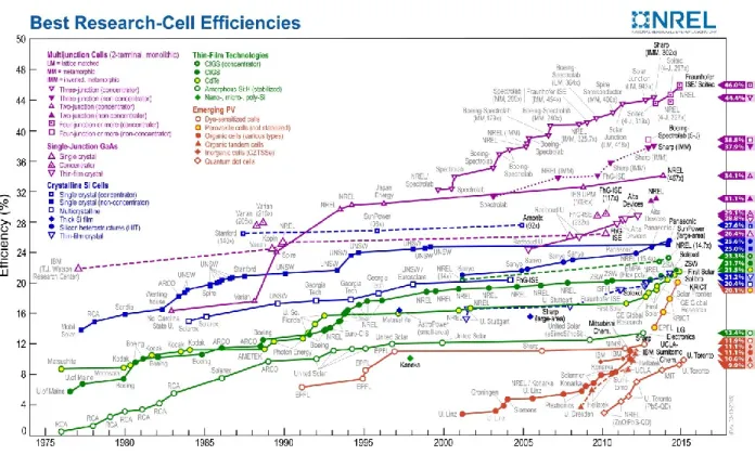
displays.6 Organic solar cells are experiencing fast paced growth with efficiencies high enough or near high enough for commercialization (Figure 1.3).7 Most relevant to the work to be presented here, organics have also become an attractive option for transistor and switch type applications relevant to computer technology.
Figure 1.3 – Champion Solar Cell Efficiencies Based on Solar Cell Type
6
1.2.2 Properties of Organics for Electronic Applications
There are strong advantages to utilizing organic materials in transistors as well as other electronic applications. Many facile processes have been developed for the deposition of organics, from the basics of spin-casting and solution soaking to more complex patterning methods. Solution processibility of many organics allows for mass-producible deposition methods such as flow-coating and ink-jet printing.8 Taking advantage of the self-assembly properties of organics can lead to easy-to-produce assemblies. For example, pentathiophene derivatives are found to assemble into micron sized conductive islands when prepared in
Langmuir-Blodgett films.9 Many of these processes can be low cost, accomplished by relatively basic equipment and requiring little more than the active material and solvent or surfactant.
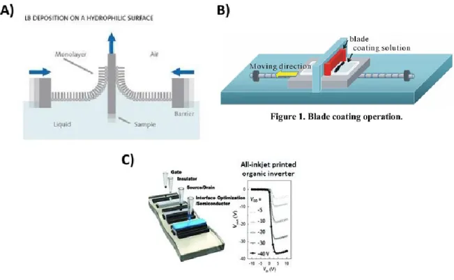
Figure 1.4 – Solution Processible Techniques for Large Scale OPV Production.
Representation of several solution processible techniques for mass production of organic photovoltaics. A)
Formation of Langmuir-Blodgett films from a solution.10B) Blade coating of organic PV (OPV) films from
solution.11 Copyright 2013, Scientific Research Publishing. C) Representation of fabrication process and output of
7
Another advantage is the functionalizability of organic materials. Sometimes simple chemical reactions and design principles can modify organic materials and dramatically change their properties. In one study, attaching a tetrathiafulvalene (TTF) moiety onto different positions along a oligo(phenylene ethynylene) (OPE) backbone significantly alters the bandgap and
conductance of molecular wires.13 Using linear or bent OPE backbones can also change the delocalization of charges along a wire.14 Controlling the rotation of phenyl rings synthetically highlights that conductance can be tuned synthetically.15 These represent just a few examples of the capability shown in organic systems.
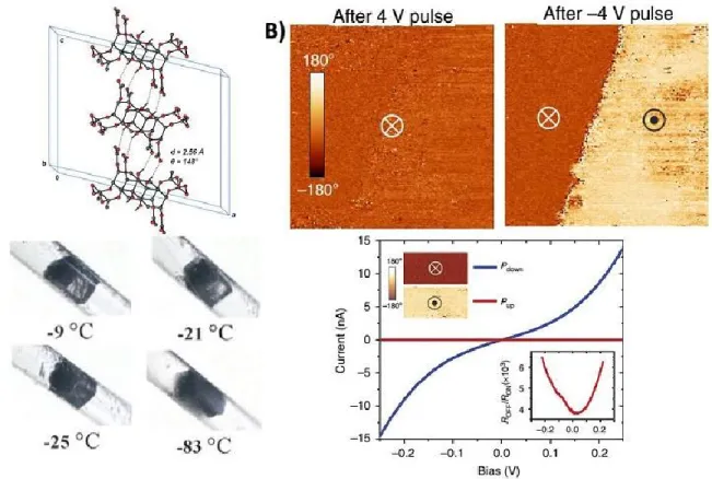
Even more impressive than these, the most dynamic organic systems contain functional groups or configurations that can be switched post-synthesis. Photochromic compounds can have conjugation established or broken, which will have large impacts on the conductivity of the molecular unit.16 Temperature can be designed to switch between polymorphic states in
tetraacetate.17 Exposure to specific chemicals (or hydrogen, in the case of pH changes) can also affect conjugation and thereby conductivity,18 and magnetic or electric fields can be used to alter spin states or electric polarizations and thereby conductivity (Figure 1.5).19 It should be stated that some silicon systems can be altered, the main way being chemical or physical doping, but in-situ alteration of their properties like those described here are rare.
8
of various appendages and organs, enabling their use in external limbs and studying diseases and events such as heart disease and strokes.22,23
Figure 1.5 – Examples of Post-Synthesis Switchable Properties in Organic Systems
Examples of post-synthesis switch properties in organic systems. A) Molecular packing in polyacene films at 18 °C, and visual representation of its polymorphism at different temperatures. Reproduced from Ref. 17 with permission
of The Royal Society of Chemistry. B) Graphene/NH3/BaTiO3/LSMO samples, measured by piezoresponse force
microscopy, showing the appearance of different electric field polarizations at different biases. The current-voltage plot underneath shows different resistances can be measured for upward (red) and downward (blue) polarizations in the sample.19 Reprinted by permission from Macmillan Publishers Ltd: Nature, Ref. 19, Copyright 2014.
9
effects are removed by studying systems in vacuum or inert environment (nitrogen, argon), but these conditions are difficult to extend to practical use. Encapsulation methods have been developed to mitigate these effects, such as depositing inorganic oxides24 or polymer layers.25 Especially with the former, care must be taken such that the encapsulating material doesn’t penetrate or otherwise impede function of the active layer.
Despite this disadvantage, constant advancements such as encapsulation continue to push organic materials to relevancy in electronics. Especially as we consider the capability to make devices on the single molecule level as will be described in the next section, a bright future is evident from applications incorporating these materials.
1.3 Molecular Electronics
Beyond bulk materials and films,a frontier of electronic devices exists at the single molecule level. Even considering the presumably soon advent of sub-10 nm transistors, molecular electronics (ME) – which is generally referred to here as utilizing organic-based molecules in single or few number of molecule junctions for electronic applications – promises a huge jump in transistor density due to devices potentially existing within a single molecule. Though more than this, molecular electronics is an exciting field because of the unique
properties that can exist in single or few number of molecule junctions. When properly executed, the synthetic control that can be had on organic molecules can be used to directly realize
dramatic property changes in molecular electronic systems.
1.3.1 Synthetic Control of Molecular Electronic Properties
10
control the charge transport through finite regimes such as tunneling and charge hopping, as seen by controlling the number of repeat units in OPE chains.26 Functional groups can also
significantly modify the charge transport properties of similar length wires. Synthetically
inserting parallel transport pathways through a molecular wire can lead to quantum interference, either constructive or destructive, with these effects sometimes being altered with different functional groups on a common backbone.27 Due to quantized energy levels present in many organics, bias dependent current effects can be realized. Negative differential resistance and other similar alterations in the current profile of molecular electronic systems can manifest as transport becomes resonant under certain biases.28 In addition, organic systems can be designed to rectify current based on the direction of injection electrons (holes). Often this control comes from asymmetric systems, created in some cases through physical separations of n-type and p-type regions,29 other times by incorporating asymmetric regions on molecular wires.30,31
Figure 1.6 – Altering Charge Transport Mechanisms in Molecular Wires
11
1.3.2 Switchable Properties in Molecular Electronics
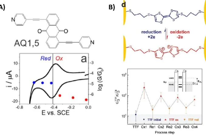
Perhaps even more powerful than the effects already described, a wide range of hysteretic and switchable properties can be realized in molecular electronic devices for potential use in single molecule transistors. These properties can start at the thin film level, such as in metal organic frameworks (MOFs) containing 7,7,8,8-tetracyanoquinodimethane (TCNQ) that can have tunable electrical properties with different TCNQ infiltration,33 and C60 films on silicon oxide substrates that have hysteretic current based on previously applied bias due to remnant charges at the C60/ silicon oxide interface.34
Figure 1.7 – Conductance Switching in Molecular Wires
A) Anthraquinone-based molecular wires in STM-BJ setup, where oxidizing/reducing the anthraquinone core
correlates with over an order magnitude change in the conductance of the wire. Reprinted with permission from Ref.
35. Copyright 2014 American Chemical Society. B) A TTF derivative in STM-BJ setup where oxidation/ reduction
of the wire changes the ratio of the conductance relative to a junction with just C8 molecules present (GTTF/GC8).
12
Because of their simplified transport pathways, molecular wires can amplify these effects from switchable events. Utilizing the oxidation/reduction of an anthraquinone core, molecular wires in a scanning tunneling microscopy (STM) setup can exhibit over an order of magnitude alteration in current.35 Redox reactions affecting TTF units in molecular wires were also shown to affect current and sheet resistance in connected networks of gold nanoparticles (Figure 1.7).36 Similar to redox switching, controlling the charges on zwitterions attached to a surface is expected to be able to modulate current.33 Organic fluorescent logic gates were designed to be able to respond to multiple stimuli– glutamate, zinc, and pH – and form molecular logic ‘AND’ gates that influence the fluorescence output based on the inputs.37 Utilizing in-situ chemical reactions via sources such as ultraviolet (UV) light to affect conjugation in molecular wires will affect coupling of molecular units and therefore the current that can pass through them.16,38 In addition, physical mechanisms can be used to control output through molecular wires.
Mechanically stretching a junction can affect conjugation and affect current through the junctions.39–41 Altogether, a host of switches manifesting from control of the properties of organic molecular wires have been realized, highlighting the power and promise of organic-based molecules in this setup.
1.4 Organic Spintronics
13 1.4.1 Basics of Spintronics- Spin Valve
Figure 1.8 – Spin Valve
Pictorial representation of a spin valve, with a tunneling spacer separating two magnetic electrodes (represented by ‘L’ and ‘R’ for ‘left’ and ‘right’). A) Electrodes with parallel magnetization, leading to matching of spin DOS in this system at Fermi level (EF) and high current through the device. B) Electrodes with anti-parallel magnetization, leading to mismatch of spin DOS in this system at EFand low current through the device.
14
are possible. If the majority spin transported through the device is also the majority DOS in the acceptor, a large number of electrons are allowed to be transported through the junction, signifying the low resistance/ high current state of the device. Mismatch of majority spin and receptor spin DOS will result in the inability of electrons to transport through the device. Electrons will be scattered at the receptor interface, and a high resistance/ low current state will ensue.
The ideas presented in this basic picture are the functioning principles behind the spin valve (Figure 1.8). The spin valve has three parts: two metals, typically from a class of metal known as a ferromagnet which, up to its Curie temperature – the temperature at which its loses its ability to sustain a remnant magnetism upon removal of the magnetic field – maintains spin DOS after it has been manipulated via magnetic field; and an insulating (non-magnetic) tunnel barrier. The two metals are influenced by a magnetic field to change their spin state, ideally having different coercive fields to manipulate their spin states independently of the other metal. As magnetic field switches the magnetizations of the electrodes, the resistance of the overall junction will change as the electrodes have parallel or anti-parallel magnetizations. Electrons tunneling through the tunnel barrier will maintain their spin state, allowing for the electrodes and their magnetic properties to be the only comparison that influences the resistance. The effect of magnetic field due to change in resistance as a function of magnetic field is represented by the magnetoresistance (MR) of the device:
𝑀𝑅 =𝑅(𝐵) − 𝑅0
𝑅0 (1-1)
15
the sign can be either due to the properties (specifically the DOS) of the metals used. While the magnetizations of the metals will always be aligned if a large enough magnetic field is applied, due to the nature of tunneling, the electrons at the Fermi level (EF) will be the highest energy electrons and have the largest probability of transporting through a tunnel junction.
Magnetization doesn’t always correspond with DOS at EF, so it is possible to have two metals that have aligned magnetic states but either aligned or mismatched DOS. Because of this, it is possible to have positive or negative TMR in a spin valve. Knowing the DOS of the metals allows us to estimate a TMR value via Julliere’s model42:
𝑇𝑀𝑅 =𝐺⊥− 𝐺∥ 𝐺∥ =
2𝑃𝐿𝑃𝑅
1 − 𝑃𝐿𝑃𝑅 (1-2)
𝑃𝐿 = 𝑛𝐿↑− 𝑛𝐿↓ 𝑛𝐿↑ + 𝑛
𝐿
↓ 𝑃𝑅 =
𝑛𝑅↑ − 𝑛 𝑅 ↓
𝑛𝑅↑ + 𝑛 𝑅
↓ (1-3)
where G, the conductance of either the parallel (∥) magnetization condition or the anti-parallel (⊥) magnetization condition can be described by the spin polarization (P) of the two metal electrodes at EF (labeled here as ‘L’ for left electrode and ‘R’ for right electrode). The spin polarization is determined via the DOS at EF is determined by the ratio of spin ‘up’ electrons (n↑) to the spin ‘down’ electrons (n↓). The designation of ‘up’ and ‘down’ is arbitrary, as we are referring simply to two angular momenta with no distinct directionality (other than the fact that they are opposite to one another). The common notation is to consider the ‘up’ electrons to be the majority carriers, and the ‘down’ electrons as minority carriers. The equations (1-2) and (1-3) above are valid regardless of these denotations.
16
known as giant magnetoresistance (GMR), which was first seen in layered stacks of chromium and iron.43 Other effects, such as colossal magnetoresistance (CMR), an even larger MR effect than GMR when perovskite cells are used as a spacer, have been seen as well.44 This highlights the fact that many possibilities that can be built off this basic spin valve picture and can lead to many unique effects.
1.4.2 Basics of Organic Spintronics
The field of organic spintronics mostly focuses on creating unique effects in spintronic devices by replacing the tunneling spacer from the spin valve with an organic layer. At its core, this modification allows for one large advantage: organics and organic-based materials typically have higher spin delocalization lengths than their inorganic counterparts. Spin-orbit coupling interactions that would lead to spin-flipping events occur more frequently with larger atomic mass, scaling by a factor of Z4. The low atomic mass from carbon instantly reduces these effects, increasing spin diffusion length from the order of 100 nm in typical metals to as high as 102 nm in organic materials.45 Spin-orbit coupling will still ultimately reduce MR effects in longer organic systems,46 but modifying the structure of device architectures, such as taking rubrene thin films and restricting them into nanowires,47 have been able to further the spin diffusion length
improvements in certain systems. This allows for injection and transport of electron spin for finite lengths through organic materials, allowing for the spacer in the spin valve picture to become an active component in the spintronic device.
1.4.3 Organic Magnetoresistance
Simply injecting and transporting spins through an active layer bears unique
17
with one another, leading to formation and spin interaction of singlet/ triplet polarons, paired polarons, bipolarons, and singlet/triplet excitons.48 Due to these effects, ultimately the observed MR effect is no longer dependent solely on the DOS of the metals. OMAR is not a fully
understood effect, possessing positive or negative signs depending on the properties and composition of the active layer as well as the conditions under which it is measured. One
particular interesting study showed that tuning the composition of a polymer-fullerene blend can alter the presence of excitons, free charge carriers, and polarons, which thereby affects the shape and sign of the OMAR effect.48 Some experiments have shown that hyperfine coupling plays a role in the effect, where films of C60 without hydrogen groups do not exhibit OMAR but [6,6]-phenyl C61 butyric acid methyl ester (PCBM) molecules with hydrogen do.49 The
aforementioned bipolaron formation in OMAR has been used to create models that, thus far, have yielded some of the best models of OMAR in the literature.50
Figure 1.9 – Organic Magnetoresistance (OMAR) in PEDOT/C60/Al devices
18 Figure 1.10 – Coulomb Blockade
As presented in this image involving quantum dots (QDs), Coulomb blockades limit the spins that can transport through a limited transport site system, as with QDs or molecular wires. The image on the left shows that when an electron is introduced into the system on site 1, if it has the same spin as site 2, the electron cannot transport due to Pauli exclusion, and it will also scatter any other spin up electrons on site 1, effectively stopping the flow of current. In this two-QD system, the reverse bias allows for some current to flow since spin up electrons are forbidden before injection, but while they cannot transport, they also are not trapped along the wire. From Science2013, 341, 257-260. Reprinted with permission from AAAS.
One element of OMAR that has been expressed and experimentally verified is the formation of spin blockades in localized regions of organic layers. Due to Pauli exclusion principle, two electrons with same spin cannot occupy the same orbital. At least a slight
inhibition on charge transport will be seen since we no longer have spin randomized currents in these spintronic scenarios, allowing for blockades to form, as well as a lower probability of spin flipping events due to the organic materials being used. In the case of systems where the charge transport is restricted to a wire, this effect can be extremely augmented since there would be no alternate pathways for current to travel, creating a (spin) Coulomb blockade that results in very large MR effects (Figure 1.10). For example, restricting charge transport along long wires of perylene-based DXP molecules in a zeolite backbone, designed such that charge transport could not tunnel between electrodes but had to undergo charge hopping between perylene units, yields MR effects up to 2000% in sub-100 nm films.52 It should be noted here that the literature
19
same principles in OMAR apply to the wire case.53 Overall, this discussion and observation of OMAR expresses that organic films can already be manipulated to yield MR effects much larger than the tunneling based MR effects typical in spin valves.
1.4.4 Magnetic Properties from Organic Molecules
Even beyond this, specialized organic molecules can possess inherent magnetic properties, allowing for injected spin to be manipulated within the ‘spacer’ of the spintronic device. Spin interactions have yielded ferromagnetic properties in specialized organic systems, such as films of bis-tetramethyl-piperidyl-oxyl-butadiin (BIPO).54 Ferromagnetic properties have also manifested in vanadium tetracyanoethylene complexes (V[TCNE]x), due to
antiferromagnetic coupling between the V2+ unpaired 3d electrons and the TCNE- unpaired π* electron, allowing a ferromagnetic system with a Curie temperature well above room
temperature.55 Interestingly, ferromagnetism has been expressed from non-magnetic Teflon substrates that have been cut or town. It is expected in these systems that dangling carbon bonds, generated by the break, interact constructively to yield the magnetic signal. Exposure to
hydrogen environments removes this magnetic signal, along with a theoretic analysis, giving further evidence to this dangling bond hypothesis.56
Taking advantage of similar magnetic properties in organics, multiple reports have suggested the capability of organic systems to manipulate spin current such that they exhibit inherent spin polarized transport. A few mechanisms exist to suggest how this can be possible. Chiral polymers represent a unique test bed as transport through these molecules results in a system similar to a magnetic coil. Magnetic coils are known from basic electricity and
20
exhibit over 80% spin polarization, detected by a variety of methods including optical analysis, cyclic voltammetry, and magnetoresistance measurements in a device, where in all cases a magnetic field is only used for spin detection.
Figure 1.11 – Organic Radicals for Spin Polarized Transport
A) Representation of TEMPO ([2,2,6,6-tetramethylpiperidin-1-yl]oxyl). B) Several radical-based molecular wires computationally showing spin-polarized transport states by Herrmann et al. Reprinted with permission from Ref. 59. Copyright 2010 American Chemical Society.
21
molecule-metal interface for switchable MR properties.60 Finished devices including this
molecule have expressed 25% MR in finished devices. Ultimately, a bonafide synthetic approach to radical insertion and utilization for spin polarized transport has not yet been developed.
It should be stated that other specialized molecular systems have been theoretically predicted to exhibit spin polarized transport. The design principles, such as coupling metal centers to conjugated sheets28 or the effect of paramagnetic metal centers to phthalocyanines and porphyrins61 provide evidence toward systems that may have strong spin interaction. The
difficulty in these systems are twofold – many of the experimentally predicted systems are difficult to be synthesized, and the spin polarized DOS predicted from many of these calculations would be difficult to realize outside of the low temperature, high magnetic field (3 Tesla and higher) conditions assumed in the calculation. The porphyrin molecules studied in this work, while slightly different from the fused porphyrin rings used in Cho et al., attempt to use this metal center- conjugated organic system approach for inherent spin transport properties.
1.4.5 Interface Considerations in Organic Spintronics
It should be noted that the MR effects in the chiral systems described above, which show high spin polarized transport through the organic molecule, ultimately yield low-MR effects (<10%) when a second electrode is attached. This highlights the fact that electrodes and interfaces can play a significant role in spin scattering effects, potentially leading to the
22
of spins through the organic is the rate limiting step in this problem, not the injection of the electrons, and since majority and minority carriers transport equally ‘slowly’, a limited number of majority and minority carriers can transport through the junction at a time. Therefore, even if a large spin polarization exists in a metal, the majority carriers do not transport quickly enough through the organic film to allow the polarization to be realized in the second electrode, and the measured spin polarization at the second electrode (as well as resulting MR effect) will be significantly lower.
One notable solution to get around the conductivity mismatch problem is to utilize a tunnel barrier for electron injection into the organic active layer. Tunneling preserves the spin of electrons, and given that it is an even higher resistance transport mechanism than transport through an organic medium (assuming the organic isn’t purely insulating), the rate limiting step for transport now becomes the tunneling barrier. While the overall resistance of the device will be raised, the spin polarization will be preserved through the organic layer, allowing for organic materials to be effectively used in spintronic settings.
23
Figure 1.12 – Engineering Spintronic Effects at Zinc Methyl Phenalenyl (ZMP) Interfaces
A) Reduction of neutral ZMP leads to an unpaired electron in the conjugated network. B) Device MR output, showing that the presence/ absence of this unpaired electron can influence a spintronic effect at the interface. Reprinted by permission from Macmillan Publishers Ltd: Nature, Ref. 60, Copyright 2013.
Several studies have demonstrated that specific interface effects can be used to effectively design organic spintronic systems with good output, even without these tunnel barriers for spin injection. So-called “spinterfaces” can be generated between organic layer and metal electrode to have realistic impacts on the output of an organic spintronic device. In the case of C60 films on iron, it was discovered that the 3d states of the iron layer
24
finished devices.66 In addition, as mentioned previously, films of ZMP can be reduced at an interface due to electron exchange with an electrode, producing an anionic radical in the ZMP molecule (Figure 1.12).60 This unpaired radical will change the magnetic properties and interactions of the molecule at the interface, and is experimentally shown to yield 25% MR in finished devices.
1.4.6 Spintronics from Controlling Spin State in Organic-Based Molecules
Much of organic spintronics focuses around the injection and extraction of electron spin in an organic layer, manipulating the spin state of current in the active layer and obtaining switchable properties from this. However, included in this topic of spintronics are systems where changing the spin state of the organic layer changes the properties of the molecule and,
potentially, the current passed through it. Electronically labile molecules with redox active metal centers are typical candidates for these effects. Specifically, d-valence metals such as cobalt, iron, manganese, rhodium, iridium, and copper have been seen in various organic-based
molecules to change spin states, a change that can also change some of the other properties of the system.67
25 Figure 1.13 – Organic Magnetic Effects
Diagrams representing the basics of spin crossover, mixed valency, and valence tautomerism. Images designed by David Schultz (NC State).
26
A more complex scenario occurs in a class of molecules known as valence tautomers (VTs). While undergoing the same low-spin to high-spin transition as SCO molecules, the transition in VTs is due to an intramolecular electron exchange between metal and ligand,
oxidizing or reducing the metal and correspondingly changing its spin state. Cobalt metal centers are strong VT candidates because of this; their neutral d7 valence shell lends itself to a high-spin configuration, whereas removing an electron from the d-shell would lend well to a low-spin configuration where all electrons could be paired.70 Such a switch would change both the magnetic properties of the VT as well as the current properties, with external switches such as light, heat, magnetic field or electrical field allowing for such a switch.
1.5 Designing Devices with Organic-Based Materials
The various examples described above show that adapting organic molecules for electronic and spintronic applications can have many advantages. The potential for switches, transistors, and molecular magnets, can all be realized through the design and implementation of organic-based molecular devices. As may also be apparent, one of the largest challenges with molecular electronics/ spintronics and the implementation of these promising effects in
27
polarization, and electronic/ spintronic coupling – have been seen or are expected to be most pronounced in monolayers, wires, or single/few number of molecule devices, where these defects, pinholes, and other fragilities will be most pronounced. Altogether, reproducing organic devices with inorganic fabrication processes is not always a perfect process. For both the efforts of scaling down device size and for seeing potentially more dramatic properties from out
systems, especially at the single molecule level, special consideration must be made in device fabrication in order to realize the effects, especially in a practical setting.
1.5.1 Techniques for Designing Molecular Electronic Devices
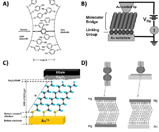
Figure 1.14 – Molecular Electronic Junctions
Several examples for forming direct contact to an organic monolayer, including A) break junctions (Reprinted with
permission from Ref. 72. Copyright 2004 American Chemical Society), B) conductive-atomic force microscopy
(cAFM) (Reprinted with permission from Ref. 73. Copyright 2011 American Chemical Society), C) gallium-indium
drop junctions (EGaIn) (Reprinted with permission from Ref. 74. Copyright 2014 American Chemical Society), D)
28
Much effort has been devoted to designing molecular junctions to realize the unique electrical and magnetic properties of organic based molecules. A host of techniques such as break junctions,72 atomic force microscopy with conductive cantilevers,73 mercury-drop electrodes, and gallium-indium drop junctions (EGaIn)74 have been used to analytically study organic systems, incorporating them into non-destructive electrical junctions and seeing the desired effects (Figure 1.14). However, these techniques are purely analytic and, at present, restricted in their possible use due to requiring either dangerous materials or highly specialized equipment for their implementation.
Figure 1.15 – Molecular Electronics Devices Prepared with Buffer Layers.
A) Devices incorporating solution processable PEDOT:PSS as a buffer layer. Reprinted by permission from
Macmillan Publishers Ltd: Nature, Ref. 75, Copyright 2006. B) Device architecture incorporating solution
processable reduced graphene oxide (rGO) for transparent electrodes.76 Copyright © 2013, Wiley-VCH Verlag
GmbH & KGaA.
29
interact metal and molecule directly at interfaces to exhibit unique effects in certain systems. For full realization of the effects organic materials can bring into the electronic/spintronic realm, the interface must be preserved and carefully tuned, and adding buffer layers only reduces the possibilities and benefits that exist from this exercise. Utilizing techniques that allow electrode deposition directly onto our systems without destroying them will offer the largest possible benefit toward dynamic single molecule systems.
1.5.2 Soft Lithography and Transfer Printing in Molecular Electronics
A recent focus for designing molecular electronic architectures with chemically bound metal contacts falls under the general title of soft lithography. The basic premise of these techniques involves some form of a transfer substrate, often times a polymer, that brings a metallic electrode into ‘soft’ contact (i.e. physical contact at ambient conditions) with an organic layer. The transfer layer may be sacrificial, as is typical in transferring plasma-enhanced
chemical vapor deposition (PECVD) grown graphene where a poly(methyl methacrylate) (PMMA) layer or other polymer layer is dissolved to expose the graphene,78 or it may be reusable in the case of a transfer process such as developed by John Rogers’ group.79 In either case, the technique usually relies on standard lithographic patterning of metal contacts on robust films and materials – polymers or silicon wafers are typical – and transferring these metals and materials using soft lithographic techniques onto the more ‘fragile’ organic monolayers and films.
30
interface and allow for strong coupling that can potentially lead to strong electron (hole) injection and effects such as the “spinterface” effects described previously. It should be noted that there is evidence of size limitations and effects of even these soft lithographic processes due to the more frail nature and other properties of certain organic systems.81 This fact will motivate studies throughout this work in analyzing the effects of different architectures and fabrication techniques on organic systems.
1.6 Research Overview
The goal of this work is to design and study unique organic-based molecules in single (or few number of) molecule device settings to study their electrical and spin transport properties, with a sub-goal of facilitating their use to practical electronic applications via facile and scalable lithographic processes. These goals necessitate two research focuses – incorporating the
molecules into settings for single molecule studies, and analyzing the architectures and processes used to incorporate these molecules into electrical devices to understand their impacts. As will be expressed, understanding the consequences of device processing and architecture is paramount if a true understanding of the organic molecules incorporated into them is to be achieved. Using the understanding of these device architectures, interesting effects in these unique molecules can be isolated and interpreted.
This work will present several sets of molecules, some basic, some with interesting transport and spin properties, toward incorporation into molecular junctions via soft lithographic techniques. Chapter 2 will show work with organometallic compounds possessing unique single molecule spin transitions – an iron spin crossover (FeSCO) compound, and a cobalt
bis(dioxylene) valence tautomer complex (CoVT. Establishing techniques to study spin
31
its spin properties. Chapter 3 will introduce a basic molecular unit – phenylenedithiols – that is used to study the impacts of a particular soft lithographic process, nanotransfer printing (nTP), on aromatic compounds. Chapter 4 will then build off the knowledge of nTP, using the technique to study molecular wires from multi[(porphinato)metal] oligomers. Special focus is given here on forming molecular wires with the complex oligomers used and, once nTP is utilized in making electrical junctions, the effects of metal center on transport properties through the wire. Chapter 5 will expand on soft lithographic techniques to attempt at forming macroscopically accessible molecular junctions for temperature dependent and spin measurements through the molecular wires as well as toward the sub-goal of practical applicability. Finally, Chapter 6 will suggest modifications based off the findings of this work toward designing more robust
32
1.7 References
(1) Schaller, R. R. IEEE Spectr. 1997, 34, 52–59.
(2) Hruska, J. Moore’s Law is dead, long live Moore's Law
http://www.extremetech.com/extreme/203490-moores-law-is-dead-long-live-moores-law. (3) Sun, X.-H.; Chen, Y. J. Parallel Distrib. Comput. 2010, 70, 183–188.
(4) Royal Swedish Academy of Sciences The Nobel Prize in Chemistry 2000 http://www.nobelprize.org/nobel_prizes/chemistry/laureates/2000/press.html. (5) Kearns, D.; Calvin, M. J. Chem. Phys. 1958, 29, 950.
(6) Barrietos, M. C. LG unveils 2015 OLED TV line-up, home appliances, and G Flex 2 http://www.gadgetsmagazine.com.ph/events/ces-2015-lg-unveils-2015-oled-tv-line-up-home-appliances-and-g-flex-2.html.
(7) National Renewable Energy Laboratory Best Research-Cell Efficiencies http://www.nrel.gov/ncpv/.
(8) Teichler, A.; Perelaer, J.; Schubert, U. S. J. Mater. Chem. C 2013, 1, 1910–1925. (9) Hendriksen, B. L. M.; Martin, F.; Qi, Y.; Mauldin, C.; Vukmirovic, N.; Ren, J.;
Wormeester, H.; Katan, A. J.; Altoe, V.; Aloni, S.; Fréchet, J. M. J.; Wang, L.-W.; Salmeron, M. Nano Lett. 2011, 11, 4107–12.
(10) Biolin Scientific Langmuir, Langmuir-Blodgett and Langmuir-Schaefer Technologies http://www.biolinscientific.com/ksvnima/technologies/?card=KT1 .
(11) Chen, K.; Yeh, H.; Chen, H.; Liu, T.; Huang, S.; Wu, P.; Tiu, C. Adv. Chem. Eng. Sci.
2013, 3, 105–111.
(12) Chung, S.; Jang, M.; Ji, S.-B.; Im, H.; Seong, N.; Ha, J.; Kwon, S.-K.; Kim, Y.-H.; Yang, H.; Hong, Y. Adv. Mater. 2013, 25, 4773–4777.
(13) Wei, Z.; Li, T.; Jennum, K.; Santella, M.; Bovet, N.; Hu, W.; Nielsen, M. B.; Bjørnholm, T.; Solomon, G. C.; Laursen, B. W.; Nørgaard, K. Langmuir 2012, 28, 4016–4023. (14) Terao, J.; Wadahama, A.; Matono, A.; Tada, T.; Watanabe, S.; Seki, S.; Fujihara, T.;
Tsuji, Y. Nat. Commun. 2013, 4, 1691.
(15) Venkataraman, L.; Klare, J. E.; Nuckolls, C.; Hybertsen, M. S.; Steigerwald, M. L. Nature
33
(16) Jia, C.; Wang, J.; Yao, C.; Cao, Y.; Zhong, Y.; Liu, Z.; Liu, Z.; Guo, X. Angew. Chem. Int. Ed. 2013, 52, 8666–8670.
(17) Mehta, G.; Sen, S. Chem. Commun. 2009, 5981–5983.
(18) Hong, J.-Y.; Chang, Y.-M.; Chuang, C.-H.; Li, K.-S.; Jhang, Y.-C.; Shiu, H.-W.; Chen, C.-H.; Chiang, W.-C.; Lin, M.-T. J. Phys. Chem. C 2012, 116, 21157–21161.
(19) Lu, H.; Lipatov, A.; Ryu, S.; Kim, D. J.; Lee, H.; Zhuravlev, M. Y.; Eom, C. B.; Tsymbal, E. Y.; Sinitskii, A.; Gruverman, A. Nat. Commun. 2014, 5, 5518.
(20) Tseung, A. C. C.; King, W. J.; Wan, B. Y. C. Med. Biol. Eng. 1971, 9, 175–184. (21) Bettinger, C. J.; Bao, Z. Polym. Int. 2010, 59, 563–567.
(22) Liao, C.; Zhang, M.; Yao, M. Y.; Huy, T.; Li, L.; Yan, F. Adv. Mater. 2014, Early View. (23) Xu, L.; Gutbrod, S. R.; Bonifas, A. P.; Su, Y.; Sulkin, M. S.; Lu, N.; Chung, H.-J.; Jang,
K.-I.; Liu, Z.; Ying, M.; Lu, C.; Webb, R. C.; Kim, J.-S.; Laughner, J. I.; Cheng, H.; Liu, Y.; Ameen, A.; Jeong, J.-W.; Kim, G.-T.; Huang, Y.; Efimov, I. R.; Rogers, J. A. Nat. Commun. 2014, 5, 3329.
(24) Sarkar, S.; Culp, J. H.; Whyland, J. T.; Garvan, M.; Misra, V. Org. Electron. 2010, 11, 1896–1900.
(25) Logothetidis, S.; Laskarakis, a.; Georgiou, D.; Amberg-Schwab, S.; Weber, U.; Noller, K.; Schmidt, M.; Küçükpinar-Niarchos, E.; Lohwasser, W. Eur. Phys. J. Appl. Phys. 2010, 51, 33203.
(26) Lu, Q.; Liu, K.; Zhang, H.; Du, Z.; Wang, X.; Wang, F. ACS Nano 2009, 3, 3861–3868. (27) Vazquez, H.; Skouta, R.; Schneebeli, S.; Kamenetska, M.; Breslow, R.; Venkataraman, L.;
Hybertsen, M. S. Nat. Nanotechnol. 2012, 7, 663–667.
(28) Chen, Y.; Hsu, S.; Kaun, C.; Lin, M. J. Phys. Chem. C 2014, 118, 21199–21203. (29) Cayre, O. J.; Chang, S. T.; Velev, O. D. J. Am. Chem. Soc. 2007, 129, 10801–10806. (30) Díez-Pérez, I.; Hihath, J.; Lee, Y.; Yu, L.; Adamska, L.; Kozhushner, M. A.; Oleynik, I.
I.; Tao, N. Nat. Chem. 2009, 1, 635–641.
(31) Ho, G.; Heath, J. R.; Kondratenko, M.; Perepichka, D. F.; Arseneault, K.; Pézolet, M.; Bryce, M. R. Chem. Eur. J. 2005, 11, 2914–2922.
34
(33) Siemeling, U.; Memczak, H.; Bruhn, C.; Vogel, F.; Träger, F.; Baio, J. E.; Weidner, T. Dalton Trans. 2012, 41, 2986–2994.
(34) Siebeneicher, P.; Kleemann, H.; Leo, K.; Lüssem, B. Appl. Phys. Lett. 2012, 100, 193301. (35) Baghernejd, M.; Zhao, X.; Ornso, K. B.; Fueg, M.; Moreno-Garcia, P.; Rudnev, A. V.;
Kaliginedi, V.; Vesztergom, S.; Huang, C.; Hong, W.; Broekmann, P.; Wandlowski, T.; Thygesen, K. S.; Bryce, M. R. J. Am. Chem. Soc. 2014, 136, 17922–17925.
(36) Liao, J.; Agustsson, J. S.; Wu, S.; Schönenberger, C.; Calame, M.; Leroux, Y.; Mayor, M.; Jeannin, O.; Ran, Y.-F.; Liu, S.-X.; Decurtins, S. Nano Lett. 2010, 10, 759–764.
(37) Hettie, K. S.; Klockow, J. L.; Glass, T. E. J. Am. Chem. Soc. 2014, 136, 4877–4880. (38) Perrin, M. L.; Frisenda, R.; Koole, M.; Seldenthuis, J. S.; Gil, J. A. C.; Valkenier, H.;
Hummelen, J. C.; Renaud, N.; Grozema, F. C.; Thijssen, J. M.; Dulić, D.; van der Zant, H. S. J. Nat. Nanotechnol. 2014, 9, 830–834.
(39) Franco, I.; Solomon, G. C.; Schatz, G. C.; Ratner, M. A. J. Am. Chem. Soc. 2011, 133, 15714–15720.
(40) Kiguchi, M.; Ohto, T.; Fujii, S.; Sugiyasu, K.; Nakajima, S.; Takeuchi, M.; Nakamura, H. J. Am. Chem. Soc. 2014, 136, 7327–7332.
(41) Su, T. A.; Widawsky, J. R.; Li, H.; Klausen, R. S.; Leighton, J. L.; Steigerwald, M. L.; Venkataraman, L.; Nuckolls, C. J. Am. Chem. Soc. 2013, 135, 18331–18334.
(42) Julliere, M. Phys. Lett. A 1975, 54, 225–226.
(43) Baibich, M. N.; Broto, J. M.; Fert, A.; Nguyen Van Dau, F.; Petroff, F. Phys. Rev. Lett.
1988, 61, 2472–2475.
(44) Ramirez, A. P. J. Phys. Condens. Matter 1997, 9, 8171–8199.
(45) Zhang, X.; Mizukami, S.; Kubota, T.; Ma, Q.; Oogane, M.; Naganuma, H.; Ando, Y.; Miyazaki, T. Nat. Commun. 2013, 4, 1392.
(46) Tran, T. L. A.; Le, T. Q.; Sanderink, J. G. M.; van der Wiel, W. G.; de Jong, M. P. Adv. Funct. Mater. 2012, 22, 1180–1189.
(47) Alam, K. M.; Bodepudi, S. C.; Starko-Bowes, R.; Pramanik, S. Appl. Phys. Lett. 2012, 101, 192403.


![Figure 2.7 – Cobalt bis(dioxylene) Molecule [CoVT] and its Valence Tautomer Transition Molecular configurations for CoVT before and after VT transition, induced by temperature and light (at low T)](https://thumb-us.123doks.com/thumbv2/123dok_us/8326215.2207810/80.918.183.735.683.899/dioxylene-molecule-tautomer-transition-molecular-configurations-transition-temperature.webp)
