IMAGING ULTRAFAST DYNAMICS IN NANOMATERIALS USING SPATIALLY-SEPARATED PUMP-PROBE MICROSCOPY
Michelle M. Gabriel
A dissertation submitted to the faculty of the University of North Carolina at Chapel Hill in partial fulfillment of the requirements for the degree of Doctor of Philosophy in the
Department of Chemistry.
Chapel Hill 2015
Approved by:
iii ABSTRACT
Michelle M. Gabriel: Imaging Ultrafast Dynamics in Nanomaterials Using Spatially-Separated Pump-Probe Microscopy
(Under the direction of John M. Papanikolas)
Understanding the fundamental physics of nanomaterials is critical for the advancement and rational design of new nanotechnologies. On the nanoscale, differences between individual structures, and even variations between different spatial locations within the same structure, can have a significant impact on the functional properties of nanomaterials and the electronic performance of nanodevices; yet much of our knowledge of nanostructure function is inferred from measurements that average over entire structures or integrate over long times. The existence of multiple conformations or structures within an ensemble, which often exhibit different dynamical behaviors, shroud the underlying dynamics, making it difficult to reach meaningful and quantitative conclusions.
iv
v
vi
AKNOWLEDGEMENTS
First of all, I would like to express my deepest gratitude to my research advisor, Dr. John Papanikolas. Joining his lab was easily one of the best decisions I’ve ever made and I will always be grateful for his guidance, patience, and wacky sense of humor (and mostly for putting up with mine). I would also like to thank Dr. Ralph House and Dr. Brian Mehl and Dr. Justin Kirschbrown for their initial development of the microscope, and for their help when I first joined the Papanikolas group. Extra thanks goes to Justin for his collaboration and support on my initial projects and surprisingly, for actually keeping me sane. I’d also like to thank all of the members of the Papanikolas group, especially Emma Cating and Dr. Erik Grumstrup for their help and advice with the spatially-separated microscopy projects. Additional recognition is required for Dr. James Cahoon for his guidance and the rest of his group for providing silicon nanowire samples and helping with COMSOL, lithography, and various other projects.
I’d also like to express my gratitude to my entire committee, especially Dr. Mark Wightman for my first summer in Chapel Hill and first impression of research at UNC and for his continued support over the years.
vii
TABLE OF CONTENTS
LIST OF TABLES ... xi
LIST OF FIGURES ... xii
LIST OF ABBREVIATIONS ... xx
LIST OF SYMBOLS ... xxii
CHAPTER 1: INTRODUCTION ... 1
1.1 Motivation ... 1
1.2 Overcoming Heterogeneity ... 2
1.2.1 Time-Resolved Spectroscopy ... 2
1.2.2 Microscopy Methods ... 3
1.2.3 Combining Temporal and Spatial Resolution ... 4
1.3 Chapter Overview ... 4
REFERENCES ... 6
CHAPTER 2: INSTRUMENTATION ... 12
2.1 Microscope Description ... 12
2.1.1 Performance Characteristics ... 15
2.1.2 Transient Absorption ... 18
2.1.3 Lock-in Detection ... 20
2.2 Spatially-Separated Alignment and Calibration... 22
2.3 Data Collection Modes ... 29
viii
2.3.2 Spatially-Separated Pump-Probe Configuration ... 31
REFERENCES ... 34
CHAPTER 3: DIFFRACTION-LIMITED TRANSIENT ABSORPTION MICROSCOPY... 35
3.1 Introduction ... 35
3.2 Variation in Dynamical Behavior across an Ensemble ... 37
3.3 Variation in Dynamics across Single Structures ... 40
3.4 Transport through Structures ... 48
REFERENCES ... 50
CHAPTER 4: DIRECT IMAGING OF FREE CARRIER AND TRAP CARRIER MOTION IN SILICON NANOWIRES BY SPATIALLY-SEPARATED PUMP-PROBE MICROSCOPY ... 54
4.1 Background ... 54
4.2 Experimental ... 55
4.3 Results and Discussion ... 56
4.4 Conclusion ... 69
4.5 Acknowledgement ... 69
REFERENCES ... 70
CHAPTER 5: IMAGING CHARGE SEPARATION AND CARRIER RECOMBINATION IN NANOWIRE P-N JUNCTIONS USING ULTRAFAST MICROSCOPY ... 73
5.1 Background ... 73
5.2 Nanowire Junctions ... 75
5.3 Spatially Resolved Population Decay of Photogenerated Carriers ... 78
ix
5.5 Computational Simulations of Charge Carrier Motion
at Low and High Injection ... 85
5.6 Simulation of SSPP Images ... 89
5.7 Conclusion ... 93
5.8 Acknowledgements ... 93
REFERENCES ... 94
CHAPTER 6: IMAGING ACOUSTIC PHONON MODES IN VANADIUM DIOXIDE ... 99
6.1 Introduction ... 99
6.1.1 Vanadium Dioxide Background ... 99
6.1.2 Advantages of Pump-probe Microscopy ... 100
6.2 Imaging VO2 Phase Transition ... 100
6.2.1 Description of Experiment ... 100
6.2.2 Description of Samples ... 101
6.2.3 Power Dependent Transients ... 102
6.2.4 Spatially-Separated Pump-Probe Imaging ... 106
6.3 Probing Coherent Acoustic Behavior in VO2 NWs ... 112
6.3.1 Polarization Dependence ... 112
6.3.2 Mechanisms of Phonon Generation ... 113
6.4 Higher Frequency Modes ... 115
6.4.1 Spatial Dependence ... 115
6.4.2 Diameter Dependence ... 119
6.5 Low Frequency Modes ... 123
x
6.5.2 Experimental Results ... 125
6.6 Propagation of Acoustic Phonon Modes ... 127
6.7 Conclusions ... 131
REFERENCES ... 132
CHAPTER 7: CONCLUSIONS ... 139
7.1 Summary ... 139
7.2 Challenges and Future Directions ... 140
xi
LIST OF TABLES
Table 4.1: Parameters used to fit kinetics derived from pump-probe microscopy to a sum of three exponentials, ΔI(t)=A1e-t/τ1 + A2e-t/τ2+ A3e-t/τ3. ... 59
xii
LIST OF FIGURES
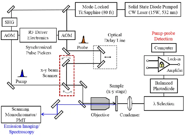
Figure 2.1: Schematic diagram of the pump−probe microscope. The pump and probe pulses are obtained from the output of a Ti:Sapphire laser operating at 80 MHz. The beam is split into the two pump and probe pulses. The pump portion is frequency doubled by SHG in a BBO crystal. Both beams are directed through synchronized AOMs to reduce the repetition rate of the pulses. The probe is sent through a mechanical delay stage (optical delay line) to vary its arrival time at the sample with respect to that of the pump. The probe beam is also directed passed a set of two scanning mirrors which vary the angle at which it enters the back aperture of the objective enabling its focal position to be adjusted laterally with respect to that of the pump. The pump and probe beams are recombined using a beam splitter and focused to diffraction-limited spots at the sample. Spatially-overlapped imaging is achieved by raster scanning the sample stage across the objective focal point while spatially-separated imaging is achieved by raster scanning the position of the probe with respect to the pump while holding the delay stage fixed. The change in transmitted probe signal is monitored with a balanced photodetector and lock-in amplifier. ... 13
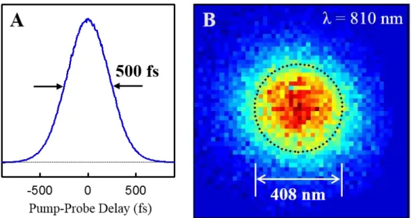
Figure 2.2: Microscope resolution. (A) Cross-correlation of the pump and probe pulses in the microscope obtained by monitoring the sum-frequency signal generated by a ZnO crystal. (B) Two-photon emission image of a 100 nm nanoparticle with 810 nm excitation. The size of the emission feature suggests that the lateral resolution is approximately 410 nm. ... 17
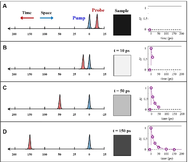
Figure 2.3: Diagram of transient absorption. (A) The transient absorption experiment in comprised of two pulses, a pump (blue) a probe (red) which is scanned in time relative to the pump pulse. In this diagram, time progresses to the left (red arrow) and the spatial coordinate is to the right (blue arrow) such that in the top configuration the probe pulse hits the sample before the pump pulse. In this configuration, the sample exhibits no pump-induced change in optical properties and the measured change in probe transmission is zero (plot on far right). (B) After the pump pulse excites the sample, a change in transmission properties of the probe occurs. In this case the sample transmits more probe light after excitation and a maximum in signal is seen just after the pump pulse arrives at the sample. (C) As the probe pulse is delayed further in time, the sample begins to relax back to it equilibrium position and a decrease in pump-induced transmission is observed. (D) After the sample has had sufficient time to completely relaxed, the observed signal response is back at baseline. ... 19
xiii
decrease, or absorption, of signal is detected (blue). If more probe light reaches the detector when the pump is ‘on’, a bleach in signal is observed. ... 21
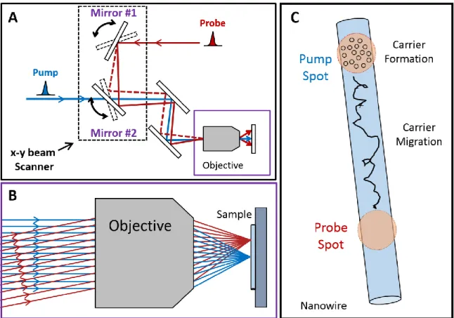
Figure 2.5: Schematic of spatially-separated pump-probe imaging. (A) The x-y beam scanner is a set of two computer-controlled mirrors with motorized actuators on both the horizontal and vertical axes. In both dimensions, Mirror #1 initially adjusts the angle of the probe beam while Mirror #2 compensates to redirect the probe beam back onto the back aperture of the objective. (B) Larger illustration of the pump and probe pulses entering the objective at different angles and focusing onto the sample at different positions. (C) Basic concept of SSPP method. A nanostructure is photoexcited in one location and probed in another location. In this illustration, electrons are excited by the pump pulse and their migration along the axis of the wire is measured via the probe pulse. ... 23
Figure 2.6: Mirror calibration. A typical calibration plot for the horizontal mirror axes. On the x axis, the horizontal position of Mirror #1 is scanned from -0.5 mm to 0.5 mm. At each position, the horizontal position of Mirror #2 is scanned. The magnitude of the signal at each (x,y) position is represented on the color scale shown to the right. The maximum value at each x position is used for a linear fit where the slope represents how far Mirror #2 must travel to compensate for motion of Mirror #1. ... 25
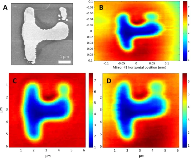
Figure 2.7: Image calibration. (A) SEM image. (B) Raw data mirror scanning image.
(C) x-y sample stage image. (D) Calibrated scanning mirror image. ... 26
Figure 2.8: Microscope spatial Imaging extent. (A) Initial image of an approximately 18 μm X 16 μm area.The circular image is a result of the beam being scanned across the last 1” mirror before the beam splitter where the pump and probe beams are recombined. This limited the spatial imaging extent to a circular area with a diameter of about 16 μm. (B) Spatial extent of the pump-probe microscope after doubling the size of the last mirror. Here the rectangular beam splitter is the limiting optic, allowing for approximately 20 μm X 20 μm uniform imaging capability. ... 28
Figure 2.9: SOPP imaging of silicon nanowire grating wires (A) Spatially-overlapped transient decay curves for points along a silicon nanowire grown according to the doping diagram on the right. The colored circles indicate where each transient trace was collected. The black curve was collected in an intrinsic region, the red curve was collected in an n-type region, and the blue curve was collected in the (ininin) grating region. This is supported by SOPP images of the same silicon nanowire in (B). The images were collected at pump-probe delays of 0 ps, 6.7 ps, 45 ps, 110 ps, and 180 ps. Each pump-probe image is depicted using a normalized color scale with the relative amplitudes indicated by the scaling factors in the bottom right corner of each frame. ... 30
xiv
experimental data. (B) SSPP images collected at the delay times denoted in the upper left of each image. The scale bar is 1 μm. Dashed black lines are guides indicating the location of the NW. Each image is depicted using a normalized color scale with the normalization factor denoted in the lower right corner. Adapted from reference 3. ... 32
Figure 3.1: Electron-hole recombination in a collection of Si NWs. (A) Pump-probe delay scans from the NW sample with 50 nm average diameter. Green traces were obtained randomly selected individual points using pump-probe microscopy. Orange curve shows decay kinetics using conventional TA spectroscopy with a broad-band continuum probe. (B) Illustration of the NW film and SEM images of the center and edge of the slide. Microscopy sampled the edges of the film while ensemble experiments sampled the more dense central regions of the slide. (C) Lifetime distributions obtained from microscopy (green) and transient absorption spectroscopy (orange) for four samples with different average diameters. (Refs. 9-11) ... 39
Figure 3.2: Transient absorption microscopy of tapered ZnO nanorods. (A) Decay scans obtained with spatially-overlapped pump and probe beams at the tip (blue) and interior points (red and green). (B) SEM images of the two structures with the locations of the delay scan marked by circles with the corresponding colors. (C) Transient absorption images showing the spatial decay of the photoinduced signal. Rapid decay is observed at the tip of the rod, while slower decay is observed in the interior sections. The spatial structure in the images is the result of the optical resonator modes supported in the cross section of the rod. (D) Optical fields associated with the resonator modes as calculated by FDFD simulations. In the larger cross-section (top) the field is distributed around the periphery of the structure, while in the smaller cross-section (bottom) the field is localized in the core. (Adapted with permission from Refs. 11,12 and 13. Copyright 2011 and 2013, American Chemical Society) ... 42
Figure 3.3: Effect of lattice strain on electron-hole recombination dynamics in Si nanowires. Pump-probe decays at different points along a NW. Location of measurements are indicated by corresponding colored circles in the SEM image (inset). At the right is a series of transient absorption images with spatially overlapped pump and probe beams that show rapid loss of the carrier population in the bent region. (Adapted with permission from Reference11,17. Copyright 2014, American Chemical Society) ... 44
Figure 3.4: Reversibility of the strain-dependent carrier recombination rate. (A)
Pump-probe images at Δt = 0 for a SiNW deposited on a flexible PDMS substrate in initial stretched (1), relaxed (2), and re-stretched (3) configurations. Scale bars are 5 μm. (B) Transient kinetic traces collected from the same position (indicated by circles in panel A) along the length of NW3 in its initial straight (1), bent (2), and straightened (3) configurations. Adapted from reference 17. ... 47
xv
a scanning mirror assembly. (B) Schematic illustration of spatially separated scanning.
(C) SEM image of the UNC logo defined in Au by electron-beam lithography; scale bar, 2 μm. (D) Left, optical transmission images obtained with the pump (I) and probe (II) beams scanned over a lower-center portion of the Au structure, as denoted by the inset box in panel C, that contains an ∼400 nm gap; scale bars, 1 μm. Red indicates maximum transmission and blue minimum transmission. Right, comparison of transmission images acquired by raster-scanning the probe beam over the entire Au structure shown in panel C using either the x-y stage (III) or the mirror assembly (IV); scale bars, 4 μm. ... 58
Figure 4.2: Normalized pump-probe microscopy decay kinetics following photoexcitation of a localized region in three different Si nanowires; NW1 (red) and NW2 (green) are intrinsic, NW3 (blue) is n-type. All three were fit to a triexponential decay (solid lines, see Table 4.1 for fitting parameters). Inset: SEM images of the three wires showing the location of pump excitation as a red circle; scale bars, 2 μm. ... 59
Figure 4.3: Time-resolved SSPP microscopy images. (A) NW1, (B) NW2, and (C) NW3. Left, SEM images of 5 μm sections of each wire centered around the pump laser excitation spot; (image sizes, 2 μm x 5 μm; scale bars, 1 μm). The location of the excitation spot is depicted by the red circle. For each sample, the tip of the wire lies beyond the top of the image. Right, series of SSPP images acquired at the pump-probe delay times denoted above each image. Location of the nanowire is depicted by the faint lines. Each image is 2 μm x 5 μm and is depicted using a normalized color scale with the relative amplitudes indicated by the scaling factors in the bottom right corner of each image. ... 63
Figure 4.4: Spatially separated pump-probe (SSPP) transient signals. (A) SSPP image obtained at t = 0 overlaid with the spatial locations, a-e, of the displaced probe beam, which correspond to separations of Δpp = 0, 1.02, 1.45, 1.83, and 2.32 μm, respectively; scale bar, 1 µm. (B) Transient signals obtained from NW2 by fixing the spatial separation, Δpp, between the pump and probe spots and scanning the pump-probe delay. The curves labeled a-e correspond to the positions indicated in panel A. Also shown is the transient signal, labeled Σ, obtained by summation of the individual SSPP signals. Individual data points are denoted by open yellow circles and the solid line is a fit to ΔI(t) = A1e-t/τ1 + A2e-t/τ2 with τ1 = 380 ps (A1 = 3.21) and τ2 = 900 ps (A2 = -1.02). ... 65
Figure 4.5: Experimental and simulated transient signals (A) Normalized SSPP transient signals obtained from NW2. The curves labeled a-f correspond to separations Δpp = 0, 1.02, 1.45, 1.83, 2.32 and 2.76 μm, respectively. (B) Analogous set of SSPP curves predicted by Eq. 4.1 using D = 18 cm2/s and τ = 380 ps. The pump and probe laser profiles have FWHM values of 350 nm and 700 nm, respectively, and are included in the simulation curves. ... 68
xvi
denoted J1, J2, and J3. Horizontal dashed lines represent junction positions estimated from growth parameters. (B) Illustration of charges present within the junction. Mobile holes (circled positive charges) in the p-type region (pink) diffuse into the intrinsic segment leaving behind fixed negatively charged acceptors. On the other side, mobile electrons (circled negative charges) in the n-type region (blue) diffuse into the intrinsic segment leaving behind fixed positively charged donors. Incomplete recombination in the intrinsic segment leads to residual free carriers at the interfaces.
(C) Finite element solutions for charge density, ρ, and electric field, E, along the axis of a p-i-n junction. The model consists a 100 nm cylindrical wire with a 2 µm p-type region, a 2 µm intrinsic region, and a 2 µm n-type region. To simulate the characteristics of the p-i-n junction, the built-in potential is calculated and applied across contacts placed at either end of the wire. Note the break in the x-axis such that only ~150 nm around each interface is displayed. ... 77
Figure 5.2: Time-resolved measurements with spatially-overlapped pump-probe microscopy. (A) Normalized decay kinetics in a p-i-n NW (J1) following localized photoexcitation within the n-type region (blue curve), the intrinsic region (green curve), and the p-type region (red). The exact locations of photoexcitation are indicated with colored circles on the SEM image in panel c. All three decays were fit (solid traces) to a sum of two exponentials with a negative offset, ΔI(t)=A1e-t/τ1+A2e-t/τ2-y0, in which the average lifetime was determined by (1/τ) Avg = [(A1/τ1)+(A2/τ2)]/(A1+A2). (B) and (C), Spatially-resolved transient absorption images collected at various pump-probe delays for p-i-n silicon NW junctions, J2 and J1, respectively. Doping profile schematics and corresponding SEM images are shown to the left of the pump-probe images. The same scale is used for SEM and pump-probe images, and scale bars are 1 µm. Dotted lines represent the approximate locations of the junction interfaces, and outlines from the SEM images are superimposed on each pump-probe image to represent approximate location of the wire. Each pump-probe image is depicted using a normalized color scale with the relative amplitudes indicated by the scaling factors at the bottom right of each image. ... 80
Figure 5.3: Time-resolved measurements with spatially-separated pump-probe microscopy. (A) and (B) Evolution of photoexcited charge carrier cloud after excitation in the center of the intrinsic region of SiNW p-i-n junctions J1 (panel A) and J3 (panel B). Top, SEM images of each wire with 1 μm scale bars. The location of the excitation spot is depicted by the red circle. Bottom, series of SSPP images acquired at the pump-probe delay times denoted in lower left of each image. Location of the NW is depicted by black outlines. Each image is displayed using a normalized color scale with the relative amplitudes indicated by the scaling factors at the lower right of each image. Vertical dashed lines mark the positions of dopant transitions in each NW. Animations of the SSPP images for each of the junctions (SAnimation-J1.gif and SAnimation-J3.gif) are provided as online supplementary information. ... 84
xvii
applied across the wire to induce an electric field with a magnitude of 106 V/m. A Gaussian distribution of carriers is generated at the center of the NW (corresponding to an axial position of 0 µm). (B-D) Charge carrier evolution along the wire axis under
(B) low injection (~1015 cm-3 electrons and holes), (C) intermediate injection (~ 1016 cm-3) and (D) high injection (~ 1017 cm-3). Hole distributions are shaded in red and electron distributions in blue with shading getting lighter at longer times. Areas where the distributions overlap appear purple. ... 87
Figure 5.5. Finite element simulation of the spatially-separated pump-probe images. (A) Illustration of the finite element simulation model, which consists of a cylindrical intrinsic NW. Metal contacts with applied bias provide the internal electric field. The surface recombination velocity (S) varies along the length of the NW to mimic the spatial variation in the recombination time and enhanced recombination in the p-type region. A Gaussian distribution of carriers (3x1019 cm-3) is generated at the center of the NW at an axial position of 0 µm. (B) Charge carrier evolution along the wire axis. Hole distributions are shaded in red and electron distributions in blue with lighter shading at longer times. Areas where the distributions overlap appear purple. Inset shows the 200 ps time slice with an expanded vertical scale to show the charge separation that occurs in the wings of the distribution. Lower panel shows time slice at 800 ps. (C) Construction of simulated image. Upper image depicts the bleach contribution arising from the free carrier (electron and hole) population. Middle image depicts the absorptive contribution (negative signal). Lower image is the simulated SSPP image which is obtained by summing the bleach and absorptive contributions.
(D) Simulated SSPP images at a series of pump-probe delays. ... 88
Figure 5.6: Mechanism for charge separation in a p-i-n NW junction under high photogenerated carrier densities.i. Carriers are generated at the center of the intrinsic region by an ultrafast laser pulse focused to a diffraction-limited spot. Photoexcited carriers are depicted as solid circles (blue for electrons and light orange for holes). Due to the high photoexcited charge carrier density, carrier-carrier interactions dominate, screening the influence of the electric field that results from the presence of fixed negative charges in the p-type region (pink) and fixed positive charges in the n-type region (blue), as well as mobile carriers that accumulate near the boundaries. ii. Carrier density is reduced by electron-hole recombination as the photogenerated carrier cloud spreads across the intrinsic region. iii. Further reduction in the photogenerated carrier density occurs as the photogenerated holes reach the n-type boundary and recombine with free electrons (open blue circles). On the opposite side, photogenerated electrons recombine with free holes (open light pink circles) from the p-type region. iv. Rapid surface recombination in p-type, with slower recombination in n-type regions. v. The reduced carrier density and large field at the boundary leads to the formation of a long-lived charge-separated state. ... 92
pump-xviii
probe image is depicted using a normalized color scale with red representing positive-going signal. The same spatial scale is used for both images with a scale bar of 2 µm. NW1 is approximately 230 nm in diameter. (B) Power-dependent transient kinetics on a single position of NW1 following localized photoexcitation (λ = 420 nm) at the point indicated by the blue circle on the zero ps delay pump-probe image. Seven transient scans are shown for pump fluences of 14 pJ/pulse, 24 pJ/pulse, 28 pJ/pulse, 33 pJ/ pulse, 38 pJ/pulse, 43 pJ/pulse and 48 pJ/pulse, with light colored traces corresponding to the lowest fluences and increasing in color saturation with increasing fluence. ... 104
Figure 6.2: Spatially-separated imaging. Spatially-separated transient absorption images collected at various pump-probe delays (0 ps, 25 ns, 50 ns, 75 ns, 100 ns, and 112.5 ns) for VO2 NW2 with the corresponding SEM image shown to the left of the pump-probe images. The red circle indicates the stationary position of the pump pulse. Scale bars are 1 µm. NW2 is approximately 330 nm in diameter. Dotted lines on the pump-probe image represent the approximate location of the NW. Each pump-probe image is depicted using a normalized color scale with the relative amplitudes indicated by the scaling factors at the bottom right of each image. ... 107
Figure 6.3: Spatial evolution of VO2 transient signal.(A) Normalized diffusion profiles for VO2 NW (NW2) following localized photoexcitation at the point indicated in Figure 6.1D. Diffusion profiles were obtained by integrating SSPP images collected at pump-probe delays of 0 ns, 12.5 ns, 25 ns, 37.5 ns, 50 ns, 62.5 ns, 75, ns, 87.5 ns, 100 ns, and 112.5 ns. (B) A plot pump-probe delay (Δt) vs β(Δt)2/(16*ln2). The diffusion constant is estimated using the slope of the weighted instrumental linear fit (solid blue line). The fit yields a slope of 1.75 X 10⁻³ µm2/ns. (C) Normalized diffusion profiles of signal for VO2 NW1 following localized photoexcitation at an individual point (not shown). Diffusion profiles were obtained by integrating SSPP images collected at pump-probe delays of 0 ns, 25 ns, 50 ns, 100 ns, 150 ns, 200 ns, 250 ns, 300 ns, 350 ns, and 400 ns. (D) A plot pump-probe delay (Δt) vs β(Δt)2/(16*ln2). The diffusion constant is estimated using the slope of the weighted instrumental linear fit (solid blue line). The fit yields a slope of 2.18 X 10⁻³ µm2/ns. ... 109
Figure 6.4: Polarization Dependence. Normalized transient absorption traces for a single point on VO2 NW1 collected with pump and probe pulses parallel to the NW axis (black trace) and with pump and probe pulses perpendicular to the NW axis (blue). ... 111
xix
Figure 6.6: (A) Offset normalized transient signals for three VO2 wires, NW4 (d = 220 nm), NW5 (d = 230 nm), and NW6 (d = 340 nm). Data for NW6 was collected at a single localized point whereas data for NW4 and NW6 represent an average of several homogeneous points along the interior of each wire. (B) Residuals for transients in 6.4A after multi-exponential decay fit for each wire. (C) Fourier transform spectra of corresponding residuals. ... 118
Figure 6.7: Diameter dependence. Fundamental (blue) and overtone (purple) mode period as a function of nanowire diameter for 5 NWs. NW1 (d = 230 nm) is represented by squares. NW3 (d = 260 nm) is represented by diamonds. NW4 (d = 220 nm) is represented by triangles. NW5 (d = 230 nm) is represented by stars and NW6 (d = 340 nm) is represented by circles. Solid spheres represent the predicted fundamental breathing mode (blue) and overtone (purple) using expressions from reference 57. ... 121
Figure 6.8: Power dependence (A) Transient decay traces at various pump fluences below the phase transition at a spatially-localized point on VO2 NW7 (B) Fourier transform spectra for the residuals (inset) of multi-exponential fits of the transients in 6.7A (C)
SEM and corresponding zero ps pump-probe delay image for NW where the red circle indicates the position where data was collected. Scale bar is 2 µm. (D) Background Subtracted transient data from Figure 6.8A where pump pulse energy is plotted as a function of pump-probe delay and the corresponding transient response is displayed on a color scale from 0 to 2.5. ... 126
Figure 6.9: Spatially-separated pump-probe images of propagating shear modes. SEM image of a region of VO2 NW6. SSPP images were collected with the pump held fixed on the position indicated by the red circle on the SEM image. The probe beam was scanned across the wire at pump-probe decays indicated above each frame. The dotted lines on each SSPP image illustrate the approximate position of the nanowire. Each image is normalized such that maximum positive-going signal corresponds to a value of 1. All images are represented on the same spatial scale. The scale bar on the SEM image is 2 μm. ... 128
xx
LIST OF ABBREVIATIONS
AFM atomic force microscopy
AOM acousto-optic modulator
BBO beta barium borate
CVD chemical vapor deposition
CW continuous wave
EHP electron-hole plasma
FET field effect transistor
FT Fourier transform
FWHM full-width-at-half-maximum
IMT insulator-to-metal transition LBO lithium triborate
MNW micro/nanowire
NA numerical aperture
NW nanowire
PMT photomultiplier tube PSD phase sensitive detection
RF radio frequency
SEM scanning electron microscopy SHG second harmonic generation SOPP spatially-overlapped pump-probe SSPP spatially-separated pump-probe
xxi
TCSPC time-correlated single photon counting TR-PES time-resolved photo-electron spectroscopy
xxii
LIST OF SYMBOLS
𝑎 radius
Aref, amplitude of the reference frequency for lock-in detection
Asig, amplitude of the signal in lock-in detection β full-width at half-maximum of diffusion profiles cL longitudinal speed of sound in a material
γpu spatial full-width at half-maximums of the pump pulse γpr spatial full-width at half-maximums of the probe pulse
d diameter
D diffusion constant
Δpp spatial separation of the pump and probe beams
Δt pump-probe delay time
E electric field
E Young’s modulus
I intensity
Jo Bessel function
L length of nanowire
λ wavelength
ν Poisson’s ratio
ξn eigenvalue for the breathing mode
ρ charge density (Chapter 5)
xxiii
σ error
recombination lifetime
τbr period of breathing mode
w weight for instrumental weighted linear fit
ϕref phase component of the lock-in reference frequency
ϕsig phase component of the signal frequency in lock-in detection
ψref waveform for the reference frequency for a lock-in detector
ψsig waveform of the chopped pump pulse train in lock-in detection
ωbr angular frequency of breathing mode
ωext angular frequency of an extensional mode
ωref angular frequency of the lock-in reference frequency
1
CHAPTER 1: INTRODUCTION 1.1 Motivation
Recent advances in technology and the associated demand for smaller and more efficient electronic, and optoelectronic devices have driven considerable research efforts focused on the optical properties of nanomaterials. As the size scale of materials becomes smaller and smaller, their properties begin to differ from those of the bulk offering a platform for the development of novel nanoscale devices. Understanding the fundamental physics of nanoscale materials is central to the developmental progress of emerging technologies.
2
rational design of new nanoscale devices. The ability to correlate function with underlying structure requires research methodologies with combined temporal and spatial resolution. The following section provides a brief overview of the evolution of spatiotemporal imaging.
1.2 Overcoming Heterogeneity
1.2.1 Time-Resolved Spectroscopy
When the focus of spectroscopic research shifted from isolated molecules in the gas phase to solvated reactions, the introduction of environmental heterogeneity within samples became a major obstacle for the reliable quantitative analysis these more complex systems. Frequency domain spectroscopy, the primary experimental technique for isolated molecules, was of limited use for the study of solvated systems. To overcome this issue, the development of new experimental techniques became vital. The ultrafast spectroscopies that emerged to meet this need enabled the observation of both solute and solvent processes on timescales as small as tens of femtoseconds. The ability to directly follow chemical dynamics in time dramatically improved the understanding of a variety of condensed phase phenomena, including energy and electron transfer processes, excited state relaxation, and solvation dynamics.
3
multidimensional coherent spectroscopies that were originally developed to address this issue enabled the assignment of spectroscopic and dynamical contributions from different sub-ensembles, these techniques are still incapable of directly correlating specific dynamical phenomena with structural or conformational variations across the ensemble without additional experimental studies or complicated theoretical calculations.
1.2.2 Microscopy Methods
With increased spatial resolution, microscopy methods bypass the heterogeneous aspects of ensemble averaging by probing materials on a structure-to-structure basis, and enabling the direct observation of the physical properties of individual particles. Over the past several decades a variety of microscopy approaches (e.g. electron, scanning probe, optical) have been implemented to reveal broad distributions in the optical, electrical, and mechanical properties in an assortment of complex systems.
4
the ensemble, uncovering phenomena such as “blinking” in molecules, proteins, and nanoparticles.19-22 While early single molecule work has had an incredible impact on our knowledge of the dynamics of sub-ensembles within complex systems, the “time-averaged” nature of detection has limited these methods to the investigation of relatively slow or steady-state processes.
1.2.3 Combining Temporal and Spatial Resolution
Advances in experimental methods with combined spatial and temporal resolution have prompted a shift from the time-averaged properties to the direct observation of the unfolding of the dynamical phenomena from which macroscopic functionality emerges. Over the past decade, transient absorption pump-probe techniques have been used in combination with optical microscopy methods to study charge carrier (electron and hole) dynamics with diffraction-limited spatial resolution in individual nanostructures4,23-39 and two-dimensional materials and structures,40-46 as well as acoustic modes and plasmonic propagation in metal nanoparticles.47-50 While access to the highest spatial resolution can be achieved through implementation of subdiffraction-limited methods based on the coupling of ultrafast laser sources with scanning probe microscopies51-60 and electron microscopies61-67, the focus of this work is on the development and application of a diffraction-limited pump-probe microscopy technique capable of measuring time-resolved dynamics including transport phenomena along individual locations within a single nanostructure. Therefore, the following chapters will be devoted to diffraction-limited pump-probe microscopy.
1.3 Chapter Overview
5
diffraction-limited pump-probe microscopy with specific emphasis on transient absorption microscopy.
Chapter 2 is devoted to the details of a new spatially-separated pump-probe microscopy technique and the microscope itself, since its development and application comprises a major component of this dissertation work.
Chapter 3 summarizes the groundwork resulting from initial efforts in the development and application of the pump-probe microscope to encompass the spatially-separated capabilities for the experiments described herein.
Chapter 4 details the initial results of the spatially-separated pump-probe microscopy technique and its application to the study of charge carrier diffusion in intrinsic silicon nanowires and doped silicon nanowires.
In Chapter 5, the microscope is used to study a more complex silicon nanowire sample fabricated with a p-type/intrinsic/n-type junction encoded along each individual nanowire. In these experiments, carrier diffusion and drift in the presence of the built-in electric field of the junction are investigated in a high carrier injection regime.
Chapter 6 demonstrates the versatility of the spatially-separated pump-probe microscope by detailing its application to the study of the insulator-to-metal transition and propagation of coherent acoustic phonon modes in vanadium dioxide nanowires.
6
REFERENCES
1 Kar, A., Upadhya, P. C., Dayeh, S. A., Picraux, S. T., Taylor, A. J. & Prasankumar, R. P. Probing Ultrafast Carrier Dynamics in Silicon Nanowires. Ieee Journal of Selected Topics in Quantum Electronics 17, 889-895, (2011).
2 Prasankumar, R. P., Upadhya, P. C. & Taylor, A. J. Ultrafast carrier dynamics in semiconductor nanowires. physica status solidi (b) 246, 1973-1995, (2009).
3 Styers-Barnett, D. J., Ellison, S. P., Mehl, B. P., Westlake, B. C., House, R. L., Park, C., Wise, K. E. & Papanikolas, J. M. Exciton Dynamics and Biexciton Formation in Single-Walled Carbon Nanotubes Studied with Femtosecond Transient Absorption Spectroscopy. The Journal of Physical Chemistry C 112, 4507-4516, (2008).
4 Song, J. K., Willer, U., Szarko, J. M., Leone, S. R., Li, S. & Zhao, Y. Ultrafast upconversion probing of lasing dynamics in single ZnO nanowire lasers. Journal of Physical Chemistry C 112, 1679-1684, (2008).
5 Grumstrup, E. M., Cating, E. M., Gabriel, M. M., Pinion, C. W., Christesen, J. D., Kirschbrown, J. R., Vallorz, E. L., Cahoon, J. F. & Papanikolas, J. M. Ultrafast Carrier Dynamics of Silicon Nanowire Ensembles: The Impact of Geometrical Heterogeneity on Charge Carrier Lifetime. The Journal of Physical Chemistry C 118, 8626-8633, (2014).
6 Ahn, Y., Dunning, J. & Park, J. Scanning Photocurrent Imaging and Electronic Band Studies in Silicon Nanowire Field Effect Transistors. Nano Letters 5, 1367-1370, (2005).
7 Howell, S. L., Padalkar, S., Yoon, K., Li, Q., Koleske, D. D., Wierer, J. J., Wang, G. T. & Lauhon, L. J. Spatial Mapping of Efficiency of GaN/InGaN Nanowire Array Solar Cells Using Scanning Photocurrent Microscopy. Nano Letters 13, 5123-5128, (2013). 8 Gu, Y., Romankiewicz, J. P., David, J. K., Lensch, J. L., Lauhon, L. J., Kwak, E. S. &
Odom, T. W. Local Photocurrent Mapping as a Probe of Contact Effects and Charge Carrier Transport in Semiconductor Nanowire Devices. Journal of Vacuum Science & Technology B: Microelectronics and Nanometer Structures 24, 2172, (2006).
9 Allen, J. E., Hemesath, E. R. & Lauhon, L. J. Scanning Photocurrent Microscopy Analysis of Si Nanowire Field-Effect Transistors Fabricated by Surface Etching of the Channel. Nano Letters 9, 1903-1908, (2009).
10 Gutsche, C., Niepelt, R., Gnauck, M., Lysov, A., Prost, W., Ronning, C. & Tegude, F. J. Direct Determination of Minority Carrier Diffusion Lengths at Axial GaAs Nanowire p-n Junctions. Nano Letters 12, 1453-1458, (2012).
7
12 Lu, H. P., Xun, L. & Xie, X. S. Single-Molecule Enzymatic Dynamics. Science 282, 1877-1882, (1998).
13 Joo, C., Balci, H., Ishitsuka, Y., Buranachai, C. & Ha, T. Advances in single-molecule fluorescence methods for molecular biology. Annual Review of Biochemistry 77, 51-76, (2008).
14 Peterman, E. J., Sosa, H. & Moerner, W. E. Single-molecule fluorescence spectroscopy and microscopy of biomolecular motors. Annual Review of Physical Chemistry 55, 79-96, (2004).
15 Nirmal, M., Dabbousi, B. O., Bawendi, M. G., Macklin, J. J., Trautman, J. K., Harris, T. D. & Brus, L. E. Fluorescence intermittency in single caadmium selenide nanocrystal. Nature 383, 802-804, (1996).
16 Le Ru, E. C. & Etchegoin, P. G. Single-molecule surface-enhanced Raman spectroscopy. Annual Review of Physical Chemistry 63, 65-87, (2012).
17 Nie, S. & Emory, S. R. Probing Single Molecules and Single Nanoparticles by Surface-Enhanced Raman Scattering. Science 275, 1102-1106, (1997).
18 Michaels, A. M., Jiang & Brus, L. Ag Nanocrystal Junctions as the Site for Surface-Enhanced Raman Scattering of Single Rhodamine 6G Molecules. The Journal of Physical Chemistry B 104, 11965-11971, (2000).
19 Basché, T., Kummer, S. & Bräuchle, C. Direct spectroscopic observation of quantum jumps of a single molecule. Nature 373, 132-134, (1995).
20 Dickson, R. M., Cubitt, A. B., Tsien, R. Y. & Moerner, W. E. On/off blinking and switching behaviour of single molecules of green fluorescent protein. Nature 388, 355-358, (1997).
21 Neuhauser, R. G., Shimizu, K. T., Woo, W. K., Empedocles, S. A. & Bawendi, M. G. Correlation between Fluorescence Intermittency and Spectral Diffusion in Single Semiconductor Quantum Dots. Physical Review Letters 85, 3301-3304, (2000). 22 Kuno, M., Fromm, D. P., Hamann, H. F., Gallagher, A. & Nesbitt, D. J. Nonexponential
“blinking” kinetics of single CdSe quantum dots: A universal power law behavior. The Journal of Chemical Physics 112, 3117, (2000).
23 Graham, M. W., Shi, S. F., Wang, Z. H., Ralph, D. C., Park, J. & McEuen, P. L. Transient Absorption and Photocurrent Microscopy Show That Hot Electron Supercollisions Describe the Rate-Limiting Relaxation Step in Graphene. Nano Letters
13, 5497-5502, (2013).
8
25 Gabriel, M. M., Kirschbrown, J. R., Christesen, J. D., Pinion, C. W., Zigler, D. F., Grumstrup, E. M., Mehl, B. P., Cating, E. E. M., Cahoon, J. F. & Papanikolas, J. M. Direct Imaging of Free Carrier and Trap Carrier Motion in Silicon Nanowires by Spatially-Separated Femtosecond Pump-Probe Microscopy. Nano Letters 13, 1336-1340, (2013).
26 Gao, B., Hartland, G. V. & Huang, L. B. Transient Absorption Spectroscopy of Excitons in an Individual Suspended Metallic Carbon Nanotube. Journal of Physical Chemistry Letters 4, 3050-3055, (2013).
27 Grumstrup, E. M., Gabriel, M. M., Cating, E. M., Pinion, C. W., Christesen, J. D., Kirschbrown, J. R., Vallorz, E. L., Cahoon, J. F. & Papanikolas, J. M. Ultrafast Carrier Dynamics in Individual Silicon Nanowires: Characterization of Diameter-Dependent Carrier Lifetime and Surface Recombination with Pump-Probe Microscopy. Journal of Physical Chemistry C 118, 8634-8640, (2014).
28 Mehl, B. P., Kirschbrown, J. R., Gabriel, M. M., House, R. L. & Papanikolas, J. M. Pump-Probe Microscopy: Spatially Resolved Carrier Dynamics in ZnO Rods and the Influence of Optical Cavity Resonator Modes. Journal of Physical Chemistry B 117, 4390-4398, (2013).
29 Mehl, B. P., Kirschbrown, J. R., House, R. L. & Papanikolas, J. M. The End Is Different than The Middle: Spatially Dependent Dynamics in ZnO Rods Observed by Femtosecond Pump–Probe Microscopy. The Journal of Physical Chemistry Letters 2, 1777-1781, (2011).
30 Schumacher, T., Giessen, H. & Lippitz, M. Ultrafast Spectroscopy of Quantum Confined States in a Single CdSe Nanowire. Nano Letters 13, 1706-1710, (2013). 31 Seo, M. A., Dayeh, S. A., Upadhya, P. C., Martinez, J. A., Swartzentruber, B. S.,
Picraux, S. T., Taylor, A. J. & Prasankumar, R. P. Understanding ultrafast carrier dynamics in single quasi-one-dimensional Si nanowires. Applied Physics Letters 100, 071104, (2012).
32 Seo, M. A., Yoo, J., Dayeh, S. A., Picraux, S. T., Taylor, A. J. & Prasankumar, R. P. Mapping carrier diffusion in single silicon core-shell nanowires with ultrafast optical microscopy. Nano Letters 12, 6334-6338, (2012).
33 Szarko, J. M., Song, J. K., Blackledge, C. W., Swart, I., Leone, S. R., Li, S. & Zhao, Y. Optical injection probing of single ZnO tetrapod lasers. Chemical Physics Letters
404, 171-176, (2005).
9
35 Grumstrup, E. M., Gabriel, M. M., Pinion, C. W., Parker, J. K., Cahoon, J. F. & Papanikolas, J. M. Reversible strain-induced electron-hole recombination in silicon nanowires observed with femtosecond pump-probe microscopy. Nano Letters 14, 6287-6292, (2014).
36 Son, B. H., Park, J. K., Hong, J. T., Park, J. Y., Lee, S. & Ahn, Y. H. Imaging ultrafast carrier transport in nanoscale field-effect transistors. ACS Nano 8, 11361-11368, (2014).
37 Blake, J. C., Eldridge, P. S. & Gundlach, L. Spatial variation in carrier dynamics along a single CdSSe nanowire. Chemical Physics 442, 128-131, (2014).
38 Gundlach, L. & Piotrowiak, P. Ultrafast Spatially Resolved Carrier Dynamics in Single CdSSe Nanobelts. Journal of Physical Chemistry C 113, 12162-12166, (2009).
39 Gundlach, L. & Piotrowiak, P. Femtosecond Kerr-gated wide-field fluorescence microscopy. Optics Letters 33, 992-994, (2008).
40 Gao, B., Hartland, G., Fang, T., Kelly, M., Jena, D., Xing, H. L. & Huang, L. B. Studies of Intrinsic Hot Phonon Dynamics in Suspended Graphene by Transient Absorption Microscopy. Nano Letters 11, 3184-3189, (2011).
41 Ruzicka, B. A., Wang, S., Liu, J., Loh, K.-P., Wu, J. Z. & Zhao, H. Spatially resolved pump-probe study of single-layer graphene produced by chemical vapor deposition [Invited]. Optical Materials Express 2, 708-716, (2012).
42 Ruzicka, B. A., Wang, S., Werake, L. K., Weintrub, B., Loh, K. P. & Zhao, H. Hot carrier diffusion in graphene. Physical Review B 82, 195414, (2010).
43 Shi, H., Yan, R., Bertolazzi, S., Brivio, J., Gao, B., Kis, A., Jena, D., Xing, H. G. & Huang, L. Exciton dynamics in suspended monolayer and few-layer MoS(2) 2D crystals. ACS Nano 7, 1072-1080, (2013).
44 Wang, R., Ruzicka, B. A., Kumar, N., Bellus, M. Z., Chiu, H.-Y. & Zhao, H. Ultrafast and spatially resolved studies of charge carriers in atomically thin molybdenum disulfide. Physical Review B 86, 045406, (2012).
45 Zhao, H., Mower, M. & Vignale, G. Ambipolar spin diffusion and D'yakonov-Perel' spin relaxation in GaAs quantum wells. Physical Review B 79, 115321, (2009).
46 Yu, G., Liu, X., Xing, G., Chen, S., Ng, C. F., Wu, X., Yeow, E. K. L., Lew, W. S. & Sum, T. C. Spatially-Resolved Ultrafast Optical Spectroscopy of Polymer-Grafted Residues on CVD Graphene. The Journal of Physical Chemistry C 118, 708-713, (2014).
10
48 Staleva, H. & Hartland, G. V. Transient absorption studies of single silver nanocubes. Journal of Physical Chemistry C 112, 7535-7539, (2008).
49 Staleva, H. & Hartland, G. V. Vibrational Dynamics of Silver Nanocubes and Nanowires Studied by Single-Particle Transient Absorption Spectroscopy. Advanced Functional Materials 18, 3809-3817, (2008).
50 Staleva, H., Skrabalak, S. E., Carey, C. R., Kosel, T., Xia, Y. N. & Hartland, G. V. Coupling to light, and transport and dissipation of energy in silver nanowires. Physical Chemistry Chemical Physics 11, 5889-5896, (2009).
51 Terada, Y., Yoshida, S., Takeuchi, O. & Shigekawa, H. Real-space imaging of transient carrier dynamics by nanoscale pump-probe microscopy. Nat Photon 4, 869-874, (2010).
52 Karki, K., Namboodiri, M., Zeb Khan, T. & Materny, A. Pump-probe scanning near field optical microscopy: Sub-wavelength resolution chemical imaging and ultrafast local dynamics. Applied Physics Letters 100, 153103, (2012).
53 Berweger, S., Atkin, J. M., Xu, X. G., Olmon, R. L. & Raschke, M. B. Femtosecond Nanofocusing with Full Optical Waveform Control. Nano Letters 11, 4309-4313, (2011).
54 Berweger, S., Atkin, J. M., Olmon, R. L. & Raschke, M. B. Light on the Tip of a Needle: Plasmonic Nanofocusing for Spectroscopy on the Nanoscale. The Journal of Physical Chemistry Letters 3, 945-952, (2012).
55 Atkin, J. M. & Raschke, M. B. Techniques: Optical spectroscopy goes intramolecular. Nature 498, 44-45, (2013).
56 Atkin, J. M., Berweger, S., Jones, A. C. & Raschke, M. B. Nano-optical imaging and spectroscopy of order, phases, and domains in complex solids. Advances in Physics 61, 745-842, (2012).
57 Smith, S., Holme, N. C. R., Orr, B., Kopelman, R. & Norris, T. Ultrafast measurement in GaAs thin films using NSOM. Ultramicroscopy 71, 213-223, (1998).
58 Nechay, B. A., Siegner, U., Achermann, M., Bielefeldt, H. & Keller, U. Femtosecond pump-probe near-field optical microscopy. Review of Scientific Instruments 70, 2758-2764, (1999).
59 Nechay, B. A., Siegner, U., Morier-Genoud, F., Schertel, A. & Keller, U. Femtosecond near-field optical spectroscopy of implantation patterned semiconductors. Applied Physics Letters 74, 61-63, (1999).
11
61 Gong, Y., Joly, A. G., Hu, D., El-Khoury, P. Z. & Hess, W. P. Ultrafast Imaging of Surface Plasmons Propagating on a Gold Surface. Nano Letters 15, 3472-3478, (2015). 62 Baum, P., Yang, D.-S. & Zewail, A. H. 4D Visualization of Transitional Structures in
Phase Transformations by Electron Diffraction. Science 318, 788-792, (2007).
63 Lobastov, V. A., Weissenrieder, J., Tang, J. & Zewail, A. H. Ultrafast Electron Microscopy (UEM): Four-Dimensional Imaging and Diffraction of Nanostructures during Phase Transitions. Nano Letters 7, 2552-2558, (2007).
64 Fukumoto, K., Yamada, Y., Onda, K. & Koshihara, S.-y. Direct imaging of electron recombination and transport on a semiconductor surface by femtosecond time-resolved photoemission electron microscopy. Applied Physics Letters 104, 053117, (2014). 65 Fukumoto, K., Onda, K., Yamada, Y., Matsuki, T., Mukuta, T., Tanaka, S.-i. &
Koshihara, S.-y. Femtosecond time-resolved photoemission electron microscopy for spatiotemporal imaging of photogenerated carrier dynamics in semiconductors. Review of Scientific Instruments 85, 083705, (2014).
66 Ortalan, V. & Zewail, A. H. 4D Scanning Transmission Ultrafast Electron Microscopy: Single-Particle Imaging and Spectroscopy. Journal of the American Chemical Society
133, 10732-10735, (2011).
12
CHAPTER 2: INSTRUMENTATION
2.1 Microscope Description
A major emphasis of the work described in this dissertation is the development and implementation of a spatiotemporal instrument incorporating a scanning mechanism whereby the position of the probe can be independently positioned relative to the pump. The introduction of this spatially-separated configuration increases the versatility of the microscope in that it can be operated in a spatially-overlapped pump-probe (SOPP) mode and a spatially-separated pump-probe (SSPP) mode. In the new SSPP mode, samples can be excited in one location and probed in another, enabling the visualization of transport properties in nanomaterials.
Figure 2.1 shows a schematic of our instrument.1-6 The primary source of radiation
begins with a solid state diode-pumped continuous wave (CW) laser (Spectra Physics: Millennia Pro-15sJ). The Millennia uses the output from a diode laser to pump a neodymium yttrium vanadate crystalline matrix (Nd:YVO4). The resulting near-infrared emission with a
wavelength of λ = 1064 is frequency doubled by second-harmonic generation in a lithium triborate (LBO; LiB3O5) crystal, which can output up to 15 W of CW radiation at a wavelength
13
14
The 532 nm CW output of the Millennia is used to pump a Ti:Sapphire laser (Spectra Physics: Tsunami). The gain medium of the laser is a sapphire crystalline matrix (Ti:Al2O3) where titanium ions (Ti3+) are substituted for a small percentage of the Al3+ ions. Absorption in the gain medium occurs over a broad range of wavelengths from 400 – 600 nm. The resulting stimulated emission generates a laser output tunable over 700 – 1000 nm. The mode-locked pulses are <100 fs in with a repetition rate of 80 MHz.
For the majority of the experiments discussed in this work, the output of the Ti:Sapphire laser is tuned to 850 nm. A portion of the 850 nm beam is split off to serve as the probe and the remainder is frequency doubled using second harmonic generation (SHG) in a beta barium borate (BBO) crystal to produce the 425 nm pump beam. Both pump and probe beams are passed through two dedicated acousto-optic modulators (AOMs), one for each beam, to reduce the repetition rate of the laser to 1-4 MHz. This step ensures that the sample returns to its equilibrium state before the next pump-probe pulse pair arrives. The AOMs (Gooch & Housego: 17389.93-FOA), are controlled using two RF drivers (Gooch & Housego: 64381.9-SYN-9.5-1 for the probe AOM and Gooch & Housego: R31389.5-5AS for the pump AOM). The drivers are synchronized using the sync output of the electronics module from the Ti:Sapphire laser (Spectra-Physics: 3995) and a delay generator (SRS-645DG).
15
aperture of a 100X microscope objective with a numerical aperture (NA) of 0.8. Focusing is achieved by adjusting the height of the objective using a nanopiezo-actuated stage, enabling remote controlled focusing of the two laser pulses to diffraction-limited spot sizes. In the case of a 425 nm pump pulse and an 850 nm probe pulse, additional steps are taken to ensure that both colors reach a focal point in the same plane. This is achieved by slightly decollimating the pump light before the objective.
After passing through the sample, light is collected using a condenser lens with a higher numerical aperture than the objective. Pump light is removed by spectral filters and the intensity of the probe beam (I) is measured using a balanced photodetector. Pump-induced changes in the probe beam (I) are extracted through the use of a lock-in detector (SRS: SR830) where the pump AOM is inhibited at a 50% duty cycle to modulate the pump beam at 10-20 kHz. This frequency also serves as the reference for the lock-in detector which will be discussed in more detail below. This transient absorption microscopy technique is remarkably sensitive, capable of detecting I/I 5x10⁻⁵.
2.1.1 Performance Characteristics
The microscope is also capable of emission detection in a forward-scatter mode, where detection comes after the sample (not shown in Figure 2.1) or in a backward-scatter mode where fluorescence emanating from emissive samples is recollected by the microscope objective, focused on the slit of a monochromator, and detected by a photomultiplier tube (PMT). Emission detection is used to measure additional performance characteristics of the microscope such as temporal resolution and spatial resolution.
16
within a zinc oxide (ZnO) crystal. Sum frequency generation is an instantaneous nonlinear process that occurs only when the pump and probe beams are focused and overlapped spatially and temporally within a nonlinear crystal. The monochromator is set to only pass the sum frequency of the pump and probe pulses which is detected using the PMT while the delay stage is scanned. A Gaussian peak in signal is observed as the two pulses cross temporally. The time resolution is taken as full-width-at-half-maximum (FWHM) the Gaussian.
17
Figure 2.2: Microscope resolution. (A) Cross-correlation of the pump and probe pulses in the microscope obtained by monitoring the sum-frequency signal generated by a ZnO crystal.
18 2.1.2 Transient Absorption
19
Figure 2.3: Diagram of transient absorption. (A) The transient absorption experiment in comprised of two pulses, a pump (blue) a probe (red) which is scanned in time relative to the pump pulse. In this diagram, time progresses to the left (red arrow) and the spatial coordinate is to the right (blue arrow) such that in the top configuration the probe pulse hits the sample before the pump pulse. In this configuration, the sample exhibits no pump-induced change in optical properties and the measured change in probe transmission is zero (plot on far right).
20 2.1.3 Lock-in Detection
Small pump-induced changes in probe transmission are monitored using lock-in detection. The lock-in amplifier is capable of extracting a small signal in an extremely noisy environment using a technique known as phase sensitive detection (PSD), which selects a single component of the signal at a specific reference frequency and phase and rejects noise signals at all other frequencies. In order to do this, the lock-in requires a reference signal, ψref, which is generally a square wave output from a function generator that the lock-in converts to a sine wave with the waveform:
𝜓𝑟𝑒𝑓 = 𝐴𝑟𝑒𝑓cos(𝜔𝑟𝑒𝑓𝑡 + 𝜙𝑟𝑒𝑓) Eq. 2.1 where Aref, ωref, and ϕref are the amplitude, frequency and phase components of the reference signal. The pump pulse train is also chopped at the same frequency and phase as the lock-in reference using a delay generator with the waveform:
𝜓𝑠𝑖𝑔 = 𝐴𝑠𝑖𝑔cos(𝜔𝑠𝑖𝑔𝑡 + 𝜙𝑠𝑖𝑔) Eq. 2.2
where Asig, ωsig, and ϕsig are the amplitude, frequency and phase components signal. Since the lock-in amplifier multiplies the reference frequency by the signal, consider the multiplication of ψref and ψsig, taking into account the product to sum identity:
𝜓𝑟𝑒𝑓𝜓𝑠𝑖𝑔 =
𝐴𝑟𝑒𝑓𝐴𝑠𝑖𝑔
2 cos[(𝜔𝑟𝑒𝑓 + 𝜔𝑠𝑖𝑔)𝑡 + (𝜙𝑟𝑒𝑓+ 𝜙𝑠𝑖𝑔)]
+𝐴𝑟𝑒𝑓𝐴𝑠𝑖𝑔
21
22
Figure 2.4 provides an illustration of how this works in our experiment. The pump (black) and probe (purple) pulses are split from the output of the Ti:Sapphire laser operating at 80 MHz and reduced to a repetition rate of 2 MHz by a pair of synchronized AOMs. Only the pump AOM is modulated at a 50 % duty cycle to a modulation frequency of 20 KHz which serves as the reference for the AOM.The probe is left unmodulated. While the balance detector measures the intensity of the entire pulse train (I), the lock-in only outputs signal that is modulated at 20 KHz and therefore only outputs ΔI. If less probe light reaches the detector when the pump pulses are ‘on’, a decrease, or absorption, of signal is detected (blue). If more probe light reaches the detector when the pump is ‘on’, a bleach in signal is observed.
In order to investigate dynamical phenomena occurring at spatially distinct locations from the initial excitation position, we have developed a pump-probe microscopy technique that uses this detections scheme while pumping a nanostructure in one position and probing it in another. The following section describes the logistics of the spatially-separated pump-probe
configuration.
2.2 Spatially-Separated Alignment and Calibration
23
24
The vertical and horizontal axes of both scanning mirrors are controlled using two motion controllers (Newport: ESP 301). With the pump and probe beams aligned through the objective at angle of 0°and focused at the same position on the sample, the position of each of the 4 mirror axes can be set to 0 on the motion controllers. The horizontal and vertical axes are then independently calibrated under the assumption that motion along one axis does not significantly alter the beam path along the other axis. This assumption is sufficiently validated by the use of gimbal-like mirror mounts that place the center of rotation at the front surface of the optic so rotational adjustments do not cause any beam translation.
25
Figure 2.6: Mirror calibration. A typical calibration plot for the horizontal mirror axes. On
26
Figure 2.7: Image calibration. (A) SEM image. (B) Raw data mirror scanning image.
27
The gear ratio’s obtained from horizontal and vertical linear fits are used as input parameters for another MATLAB script that links Mirror #1 and Mirror #2 and sets the gear ratio such that Mirror #2 automatically moves with adjustments to Mirror #1. Other input parameters tell the mirrors how fast to scan and set the scan area in units of mm of Mirror #1 actuator travel. Figure 2.7A shows an SEM image of a feature patterned on a quartz substrate. Figure 2.7B shows the raw data image of the same feature the using the scanning mirror technique. In this image, the x and y axes are plotted in terms of mm of Mirror #1 actuator movement for the horizontal and vertical actuators respectively. In order to correlate mm of actuator movement with microns of movement on the sample, we simply compare the scanning mirror image to an image collected by scanning the Queensgate x-y sample stage with the probe beam held fixed at the zero position (Figure 2.7C). Using another MATLAB script, we can convert mm of actuator movement to microns of spatial movement across the sample (Figure 2.7D) such that both images are displayed in units of microns. Figure 2.7 demonstrates distortion free imaging of the feature using both imaging techniques.
28
29
2.3 Data Collection Modes
2.3.1 Spatially-Overlapped Pump-Probe Configuration
Four modes of measurement are possible in this instrument that provide complementary information on the spatial and temporal excited state phenomena in nanomaterials. In the first, the pump and probe beams are spatially overlapped on a specific position on the sample and the pump-probe delay time is scanned using the optical delay stage. The resulting data are similar to the scan illustrated in Figure 2.3. Another example of this operational mode is shown in Figure 2.9A where SOPP transients are collected at three different points along the axis of a silicon nanowire (SiNW) grown with different doping regions as illustrated on the wire diagram on the right. Points of collection are illustrated in the diagram with color-coded circles. Here, the black trace corresponds to data collected in an intrinsic region, while the red trace was collected in the n-type region and the blue in the (ininin) grating region. The spatial resolution of the microscope enables comparison of dynamics at different regions along a single nanowire. For example, signal in the intrinsic region is much longer lived than the n-type or grating regions. This conclusion is further supported by the images in Figure 2.9B.
30
31 2.3.2 Spatially-Separated Pump-Probe Configuration
In the third mode the pump and probe beams are separated at a fixed distance (Δpp) and the delay stage is scanned analogous to the SOPP configuration (Figure 2.9A). For pump-probe experiments, it is important to note that although the probe scanning mechanism alters the path of the probe beam, the geometry is such that the excess path length introduced by the tilt of the first mirror is almost completely compensated with the tilt second mirror. As a result there is little (<0.5 ps) variation in the pump-probe delay as the probe beam is moved. Similarly, experiments using propagating surface plasmon polaritons have shown that this is also not an issue for galvo-scanner methods over length scales of several microns.7
32
33
34
REFERENCES
1 Gabriel, M. M., Grumstrup, E. M., Kirschbrown, J. R., Pinion, C. W., Christesen, J. D., Zigler, D. F., Cating, E. E., Cahoon, J. F. & Papanikolas, J. M. Imaging Charge Separation and Carrier Recombination in Nanowire p-i-n Junctions Using Ultrafast Microscopy. Nano Letters 14, 3079-3087, (2014).
2 Gabriel, M. M., Kirschbrown, J. R., Christesen, J. D., Pinion, C. W., Zigler, D. F., Grumstrup, E. M., Mehl, B. P., Cating, E. E. M., Cahoon, J. F. & Papanikolas, J. M. Direct Imaging of Free Carrier and Trap Carrier Motion in Silicon Nanowires by Spatially-Separated Femtosecond Pump-Probe Microscopy. Nano Letters 13, 1336-1340, (2013).
3 Grumstrup, E. M., Gabriel, M. M., Cating, E. M., Pinion, C. W., Christesen, J. D., Kirschbrown, J. R., Vallorz, E. L., Cahoon, J. F. & Papanikolas, J. M. Ultrafast Carrier Dynamics in Individual Silicon Nanowires: Characterization of Diameter-Dependent Carrier Lifetime and Surface Recombination with Pump-Probe Microscopy. Journal of Physical Chemistry C 118, 8634-8640, (2014).
4 Grumstrup, E. M., Gabriel, M. M., Pinion, C. W., Parker, J. K., Cahoon, J. F. & Papanikolas, J. M. Reversible strain-induced electron-hole recombination in silicon nanowires observed with femtosecond pump-probe microscopy. Nano Letters 14, 6287-6292, (2014).
5 Mehl, B. P., Kirschbrown, J. R., Gabriel, M. M., House, R. L. & Papanikolas, J. M. Pump-Probe Microscopy: Spatially Resolved Carrier Dynamics in ZnO Rods and the Influence of Optical Cavity Resonator Modes. Journal of Physical Chemistry B 117, 4390-4398, (2013).
6 Mehl, B. P., Kirschbrown, J. R., House, R. L. & Papanikolas, J. M. The End Is Different than The Middle: Spatially Dependent Dynamics in ZnO Rods Observed by Femtosecond Pump–Probe Microscopy. The Journal of Physical Chemistry Letters 2, 1777-1781, (2011).
35
CHAPTER 3: DIFFRACTION-LIMITED TRANSIENT ABSORPTION MICROSCOPY
3.1 Introduction
Disentangling signals from inhomogeneous nanomaterial samples presents a major obstacle for the rational design of new nanoscale devices. The ability to correlate function with underlying structure requires research techniques with combined temporal and spatial resolution. To this end, diffraction-limited pump-probe microscopy has been applied to studies on a particle-to-particle basis to provide insight into the distribution of phenomena emanating from each member of an ensemble. Ultrafast microscopy provides an exclusive view of the structure-function relationship, particularly in systems with variable compositions (e.g. heterojunctions and heterostructures), as well as systems with intricate shapes (e.g. ribbons or tetrapods). Many new modern nanotechnologies are even engaged to exploit secondary structure through mechanical deformation (e.g. bending or stretching) or application of electric and magnetic fields (e.g. piezoelectric) to manipulate properties of the material. The high spatial resolution of pump-probe microscopy enables characterization of the spatial variation in dynamical processes across these complicated structures. For example, the behavior at the end of a nanowire can be compared that of its interior sections. Similarly, pump-probe microscopy is advantageous for characterizing different chemical domains in heterostructures, phase-separated materials, and interfaces, which are often used to separate charges or support energy flow in photovoltaic or similar applications.