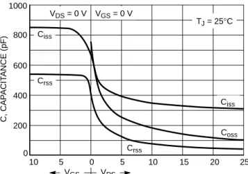
NTD3055L104. Power MOSFET 12 Amps, 60 Volts, Logic Level N Channel DPAK
Full text
Figure


Related documents
ON Semiconductor makes no warranty, representation or guarantee regarding the suitability of its products for any particular purpose, nor does ON Semiconductor assume any
It results that the arithmetic mean of the matrices could result in a poor subspace estimate despite the fact that, individually, the subspaces spanned by each matrix might
Although it can be seen that averages per sub- ject approximate to the values of the IAPS (except for set1, whose valence is greater and the arousal is lower),
In order to determine the total number of biofilm cells per unit area of the annular reactor, the number of EUB338 mix target cells per unit of the reactor’s surface area and
-channel length / effective channel length -parasitic S/D resistance / gate resistance -MOSFET scaling. Vt considerations / channel profile
Should Buyer purchase or use SCILLC products for any such unintended or unauthorized application, Buyer shall indemnify and hold SCILLC and its officers, employees,
This technology enable the power MOSFET to have better characteristics, including fast switching time, low on resistance, low gate charge and especially excellent avalanche
It has been found that a ferrite bead combined with a resistor on each MOSFET gate eliminates parasitic oscillation while minimizing switching losses.. In fact, adding a