Load-Line Regulation With Estimated Load-Current
Feedforward: Application to Microprocessor
Voltage Regulators
Angel V. Peterchev
, Member, IEEE
, and Seth R. Sanders
, Member, IEEE
Abstract—A consistent framework for load-line regulation de-sign is presented, applicable to microprocessor voltage regulators (VRs) using either electrolytic or ceramic output capacitors. With conventional feedback control, the loop bandwidth is limited by stability constraints linked to the switching frequency. The output capacitor has to be chosen sufficiently large to meet the stability re-quirement. Load-current feedforward can extend the useful band-width beyond that imposed by feedback stability constraints. With load-current feedforward, the size of the output capacitor can be reduced, since it is determined solely by large-signal and switching-ripple considerations which are shown to be less constraining than the feedback stability requirement. This work points to the feasi-bility of microprocessor VR implementations using only a small number of ceramic output capacitors, while running at sub-mega-hertz switching frequencies.
Index Terms—DC–DC power conversion, estimation, feedfor-ward systems, impedance control, load-line, microprocessors, pulsewidth modulated (PWM) power converters, regulators, tran-sient response, voltage control, voltage regulator (VR), voltage regulator module (VRM).
I. INTRODUCTION
V
OLTAGE regulators (VRs)1convert 12-V bus voltage tothe microprocessor supply rail of about 1.2 V. They have to be able to handle load transients in the range of 100 A, with rise and fall times on the order of tens of nanoseconds. At the same time the output has to be regulated tightly to a load-line with an impedance close to 1 m [2], [3].
The low conversion ratio in VRs presents a challenge since the duty ratio may saturate during large unloading transients, thus slowing down the response. Decreasing the inductor value increases the speed of response, however, this also increases the inductor current ripple and the resulting power loss. On the other hand, if a large inductor is used, the output capacitor has to be
Manuscript received January 4, 2005; revised September 8, 2005. This work was presented in part at the Power Electronics Specialists Conference (PESC), Aachen, Germany, June 20–25, 2004. This work was supported by the National Science Foundation under Grant ECS-0323615 and by the University of Cali-fornia Micro Program. Recommended by Associate Editor P. Mattavelli.
A. V. Peterchev is with the Department of Psychiatry, Columbia University, New York, NY 10032 USA (e-mail: ap2394@columbia.edu).
S. R. Sanders is with the Department of Electrical Engineering and Com-puter Science, University of California, Berkeley, CA 94720 USA (e-mail: sanders@eecs.berkeley.edu).
Digital Object Identifier 10.1109/TPEL.2006.882932
1By convention, if the VR is embedded on the computer motherboard, it is referred to as a voltage regulator-down (VRD), while if it is mounted on a sep-arate plug-in card, it is called a voltage regulator module (VRM).
made large, to sustain the load during transients. Increasing the output capacitor count drives up the VR cost and footprint. The limiting (critical) values of the power-train output capacitance and the power-train inductance, which permit tight load-line regulation, have been derived in [4]–[8], respectively. A number of topological modifications to the basic interleaved buck con-verter have been proposed to improve the transient response, while retaining high efficiency [9]–[19].
Besides these efficiency and transient considerations, the tight load-line regulation requirements present a challenge to the controller design as well. Conventional load-line regula-tion (a.k.a. adaptive voltage posiregula-tioning) sets the closed-loop output impedance equal to the output capacitor effective series resistance (ESR) [4], [5]. This method allows for the output ca-pacitance to be halved for a given transient regulation window, compared to stiff output regulation. Load-line regulation im-plementations based on feedback current-mode control [4], [5], [8] and feedback voltage-mode control with load current injection [6], [15], have been presented, using power trains with electrolytic output capacitors. Variations of these linear control approaches are commonly adopted by industry, typically using fixed-frequency pulsewidth modulated (PWM) modulation [11]. With these techniques, the nominal system closed-loop bandwidth is tightly related to the output capacitor ESR time constant [8], [16]. With typical electrolytic capacitors having such a time constant on the order of 3–10 s, it is straightfor-ward for this approach to work with conventional switching frequencies in the range of 200–500 kHz. For modern VR ap-plications, ceramic capacitors present an attractive alternative to electrolytics due to their low ESR and low effective series inductance (ESL), small footprint, and low profile. However, ceramic capacitors have ESR time constants between 20 and 200 ns, yielding the conventional load-line design framework unsuitable, since it would require a switching frequency on the order of 10 MHz [8]. Further, if ceramic capacitors with ESR matching the desired output impedance are used, their capacitance will be too low to provide adequate ripple filtering and load transient support.
The bandwidth of converters with linear feedback control is limited by stability constraints linked to the switching fre-quency [8], [16]. Extending the bandwidth can result in cost and board area savings, since it can reduce the required number of capacitors [17]. However, increasing the switching frequency to effect bandwidth extension results in additional switching losses. Nonlinear duty-ratio control techniques have been pro-posed to extend the effective bandwidth and improve transient
performance [18]–[21]. However, these approaches tend to have closed-loop performance which is difficult to predict and is sen-sitive to noise. Hysteretic control could offer fast response as well, however it is difficult to generalize to multi-phase con-verters due to ripple-cancellation effects and the lack of an in-ternal time reference for the phase shifting. Proposed multi-phase hysteretic architectures [22], [23] appear to have high sensitivity to noise, as well, due to the small amplitude of the ripple signals. Finally, load-current feedforward has been used to speed up the transient response in current-mode converters with stiff voltage regulation [5], [24]. However, in [5] it is sug-gested that fast feedback compensation can match the perfor-mance of load-current feedforward. This may be true for partic-ular converter designs but is not the case in general, as will be argued in this paper.
In this work, we extend the load-line regulation framework to encompass capacitor technologies with a wide range of time constants, including electrolytic and ceramic capacitors. In this context we identify the bandwidth limitations of feedback approaches. In particular, the required loop bandwidth is in-versely proportional to the output capacitor size. We propose and demonstrate the use of linear load-current feedforward to extend the useful control bandwidth beyond the limits imposed by feedback stability constraints. We derive the feedforward control laws for both voltage-mode and current-mode load-line control. The load-current feedforward is used to handle the bulk of the regulation action, while the feedback is used only to compensate for imperfections of the feedforward and to ensure tight dc regulation. In this case, the size of the output capacitor is determined by large-signal transient and switching-ripple considerations, and not by the feedback stability constraint. We extend previous large-signal transient analyses to derive a critical capacitance value which accounts for the capacitor time constant, controller delay, load current slew rate, and allowable load-line overshoot. It is demonstrated that for representative ceramic-capacitor VR architectures, the large-signal and ripple constraints on the output capacitor are less restrictive than the feedback stability requirement. Therefore, eliminating the feedback stability constraint by applying load feedforward can reduce the required number of output capacitors. In par-ticular, the electrolytic bulk capacitors in a VR design can be eliminated, and the voltage regulation can be fully supported by the ceramic high-frequency-decoupling capacitors in and around the microprocessor socket cavity, at sub-megahertz switching frequencies. The load-current estimate used in both the feedback and feedforward control laws is obtained via lossless inductor and capacitor current sensing.
In Section II, we generalize the load-line impedance to a dy-namic quantity which is consistent for capacitor technologies with both large (electrolytic) and small (ceramic) ESR time con-stants. Section III reviews feedback load-line control methods, extends them to a generalized load-line impedance, and identi-fies their bandwidth limitations. Section IV introduces load-cur-rent feedforward as a means of circumventing the bandwidth limitation of pure feedback control, and derives feedforward control laws for both voltage-mode and current-mode control. Section V discusses large-signal constraints on the converter load-transient performance, and identifies a minimum (critical)
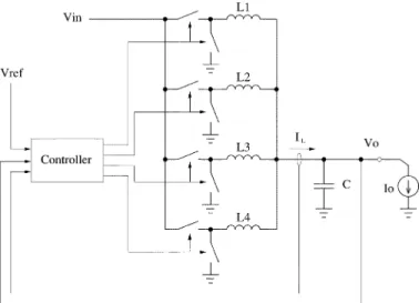
Fig. 1. Four-phase buck converter. The four phases are interleaved at 90 with respect to each other, in order to reduce the output voltage ripple and input cur-rent ripple.
capacitance value which can support the load transient. Sec-tion VI identifies requirements on the output capacitor size due to the switching ripple. Section VII compares the various con-straints on the output capacitor size, in the context of micropro-cessor VRs, and discusses load-current estimation and PWM modulator choice. Finally, Section VIII presents simulated and experimental results on feedback and feedforward control of a four-phase buck converter with ceramic output capacitors.
II. LOAD-LINEIMPEDANCEREGULATION
Fig. 1 shows the simplified structure of a representative four-phase buck converter, commonly used in microprocessor VRs [25]. In the analysis in this paper, the multiphase converter is modelled as a single-phase converter for simplicity, unless stated otherwise. Conventional load-line control, as used in microprocessor VR applications, sets the desired closed-loop impedance equal to the output capacitor ESR [4], [5]. While this approach works well with capacitor technologies with large ESR time constants , such as electrolytic capacitors, it is not applicable to small ESR time constant technologies, such as ceramic capacitors, due to their small capacitance per unit ESR [8], [16]. With ceramic capacitors, the capacitor size has to be chosen large enough so that it provides adequate ripple filtering and load transient support. Due to the small ESR time constant, this results in the ESR being much less than the desired load-line impedance . Under these circumstances, it is natural to specify the load-line impedance dynamically, so that in the low-frequency limit the output impedance is equal to , and in the high-frequency limit it converges to the capacitor ESR value . To achieve this, the load-line impedance can be set to
(1) This is a generalization of the resistive output impedance in con-ventional load-line control, where . This approach
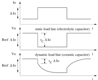
Fig. 2. Typical output voltage transient response with load-line regulation, as-suming no duty-ratio saturation occurs. Illustrated are static and dynamic load-lines, which are appropriate for electrolytic and ceramic output capacitors, re-spectively.
reconciles the use of output capacitors with ESR lower than the specified load-line impedance. The load-line is now given by
(2) In Fig. 2, the output voltage step response with a dynamic load-line (e.g., with a ceramic capacitor) is compared to that with a conventional static load-line (e.g., with an electrolytic capac-itor). Note that this load-line impedance paradigm would be consistent with an ideal capacitor with zero ESR, where 0.
It should be noted that the controller for a ceramic-capacitor power train has to be designed so that the output impedance is regulated to , and not to , since the latter approach will result in undesirable load-line overshoot. Consider, for example, the loading step in Fig. 2. Initially the output voltage will drop by due to the capacitor ESR. If the reg-ulator implements a static load-line with impedance , the controller will try to force the output voltage to drop by , instead. The controller will initially decrease the duty-ratio command, instead of appropriately increasing it to handle to loading transient. Consequently, the inductor current will initially decrease, instead of increasing, eventually making the output voltage overshoot beyond the desired load-line.
III. FEEDBACK CONTROL APPROACHES ANDTHEIRLIMITATIONS
Traditionally, feedback control approaches have been used to implement load-line regulation. Here we review these methods, extend them to the generalized impedance regulation described in Section II, and identify their bandwidth limitations.
A. Switching Stability Constraint
In fixed-frequency switching converters with feedback con-trol there is a fundamental limit on the loop-gain bandwidth
which results in stable closed-loop operation. In particular, feed-back bandwidth which approaches or exceeds the switching fre-quency may result in nonlinear behaviors such as period-dou-bling or chaos [26]. This stability constraint can be expressed as
(3) where is the feedback unity-gain frequency, and is a con-stant. According to Deslaurierset al.[27] the fundamental upper limit for naturally-sampled, triangle carrier PWM is 1/3. For practical designs 1/6 is recommended in [8]. In an in-terleaved -phase buck converter the stable bandwidth can po-tentially be extended by times, due to the reduced modulation delay [28]. However, in the presence of parameter mismatches among the phase legs, aliasing effects at the switching frequency may reduce the usable bandwidth [28]. Thus, (3) with 1/6 stands as a practical stability guideline, with the understanding that for multi-phase designs it may be on the conservative side.
B. Load-Line Feedback
This approach is based on the principle that if an error signal formed by subtracting the desired load-line trajectory from the output voltage, is fed to a high gain feedback controller, the output voltage will track the load-line. This method was discussed in [6], and replicated in [15]. It can be used with both voltage-mode and current-mode control. Similar approaches have been used in a number of commercial integrated circuits (ICs). Some commercial ICs use the inductor current, instead of the load current, to form the load-line reference signal [11]. This results is additional derivative gain of the feedback con-troller which tends to improve transient performance, provided the closed-loop system is stable. In this work, we use the load current in the definition of the load-line, and relegate the control dynamics to the feedback and feedforward control laws, which provides for a clean and flexible design framework.
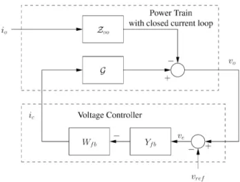
A small-signal block diagram of the load-line feedback scheme with a voltage-mode controller is shown in Fig. 3. Here (4) is the transfer function between the controller command and the output voltage, is the total power train inductance for an -phase converter, and is the series combination of the total inductor resistance and the average switch and input source resistance. The controller command incorporates the PWM modulator voltage gain, , where is the duty ratio command and is the input voltage. The open-loop output impedance is
(5) The feedback controller uses a standard PID control law, with an extra high-frequency pole 1 which ideally cancels the capacitor ESR zero
Fig. 3. Load-line feedback block diagram with voltage-mode control.
The derivative term zero and the 1 pole provide a 20 dB/dec rolloff above the cutoff frequency, to en-sure a good phase margin. Conventional design procedures can be used to choose the PID parameters to yield good phase and gain margins [29, Ch.9]. The high-frequency dynamics of the feedback loop are modelled by
(7) where lumps the effective delay of the modulator, the gate drivers, and the power switches.
From Fig. 3, the converter closed-loop output impedance is calculated to be
(8) In Appendix A, it is shown that for with load-line feedback control, the loop unity gain bandwidth has to be
(9) This observation is confirmed by the simulation results in [15]. However, as discussed in Section III, to avoid closed-loop in-stabilities, the loop bandwidth should be below the switching frequency. Combining (3) and (9) results in a trade-off rela-tion between the number of output capacitors required and the switching frequency used
(10) Thus, for a given switching frequency, the output capacitor should be selected sufficiently large to meet the stability con-straint.
C. Voltage Feedback With Finite dc Gain
This approach uses the fact that a power converter with fi-nite, nonzero dc feedback gain has a fifi-nite, nonzero closed-loop output impedance. Thus, by appropriate selection of the feed-back control law, the converter closed-loop output impedance
Fig. 4. Model of current modulator with current (inner) loop closed.
Fig. 5. Block diagram of current-mode load-line control with finite dc gain compensatorY .
can be set to a particular value. This approach is readily imple-mentable with current-mode control, while its use with voltage-mode control is not practical [8]. This method, developed for the special case of the output impedance equal to the output capac-itor ESR, was introduced in [4] and [5]. In the discussion below it is extended to the control of a general output impedance , as defined in (1).
Fig. 4 gives the model of a buck converter with a current-mode controller. Parameter is the current command provided by the voltage (outer) control loop, and is the effective cur-rent-loop gain. The curcur-rent-loop gain is modelled as
(11) where is the compensation ramp slope, and
is the switching period [29, Ch.12], [30]. Without a compensa-tion ramp 0 , the effective current-loop gain is infinite , reflecting the sliding-mode nature of the current loop.
Fig. 5 shows a control block diagram of the complete con-troller. The transfer function between the current command and the output voltage, with the current-loop closed, is
where is the number of phases. The corresponding open-voltage-loop output impedance is
(13) Note that for high current-loop gain , both (12) and (13) become independent of the inductor value , since the cur-rent loop provides for this desensitivity [29, Ch.12]. Finally, the closed-loop output impedance of the converter is
(14) where parameter models the loop delay, analogously to (7), and is the feedback control law.
Assuming a high value of the current-loop gain , ignoring the high-frequency dynamics 1 , and re-quiring , we obtain the feedback control law
(15) which is consistent with the derivation for the case of
[4], [5]. Under this control law, the voltage-loop unity gain bandwidth is
(16) Indeed, for the case has been previously identi-fied as a critical bandwidth which constrains the switching fre-quency choice [8], [16]. Analogously to Section III-B, we can combine (16) with the bandwidth stability constraint (3) to link the required output capacitance to the switching frequency
(17) Clearly, the voltage-loop bandwidth requirement (16) and the associated output capacitor constraint (17) are more relaxed compared to those for load-line feedback control given in (9) and (10), respectively. However, here we have assumed infi-nite current-loop gain. In practice, a compensation ramp may have to be introduced in the current-mode PWM modulator for stability and noise-immunity purposes, which reduces the effective current-loop gain [29, Ch.12]. If a compensation ramp is introduced, the voltage-loop control law (15) has to be modified to reflect the finite current-loop gain.
Finally, it should be pointed out that when used with peak or valley current control schemes, this method incurs a dc output voltage offset. Since the feedback loop controls the peak or valley inductor current rather than the average current in each phase, the output voltage is shifted from the reference load-line by 2, where is the peak-to-peak phase current ripple. This problem can be remedied by ap-propriately adding a slow integrator to force the average phase inductor current to equal the current command .
IV. LOAD-CURRENTFEEDFORWARDCONTROL
The load-line regulation approaches discussed in the previous sections are based on feedback, and it was shown that their
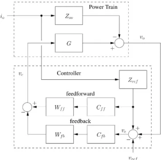
Fig. 6. Voltage-mode load-line control block diagram with load-current feedforward.
bandwidth is fundamentally limited by stability constraints. Feedforward is a control paradigm which can complement feedback by providing a fast response to load-current transients. Generally, feedforward is used to cancel the effects of known disturbances, and provide anticipative action in tracking tasks [31, Ch.3], [32, Ch.7]. For example, assume that the converter load is a current source with variable current. If we can measure or estimate the variations of the load current, we can compute the appropriate control actions that would result in the desired output load-line, without invoking feedback. In this case, the load current is an exogenous variable rather than a state variable of the converter, since the load is an independent current source. Thus, the gain and bandwidth of the feedforward are not limited by stability considerations [32, Ch.7], and therefore the feedforward can provide very fast response to load changes. The major limitation of feedforward is that to calculate the feedforward control law, a model of the power train is required [31, Ch.II.3]. Since it is virtually impossible to have an exact model of the converter, feedforward cannot provide tight regulation by itself. Therefore, to effect fast and precise regulation, a combination of feedforward and feedback should be deployed: The feedforward rapidly computes the bulk of the regulation action, while the feedback damps resonances, and compensates for imperfections of the feedforward. Load-current feedforward can be used with both voltage-mode and current-mode control, and the feedforward control laws for both cases are derived below.
A. Voltage-Mode Control
Fig. 6 shows a block diagram of the buck converter with voltage-mode line control from Fig. 3 with an added load-current feedforward path. Here, is the feedforward control law, and
models the delay of the feedforward path. The closed loop output impedance is
(19) The feedforward control law can be derived by setting the closed-loop output impedance (19) equal to the desired value
, yielding
(20) Note that if the ideal feedforward law (20) could be imple-mented, the output impedance would have the desired value and no feedback is necessary. In reality, this is impos-sible due to parameter uncertainties and the fact that con-tains delay, thus would be anticausal. A practical implemen-tation can approximate with an error
(21) Then the output impedance (19) becomes
(22) Thus, the feedforward carries out the bulk of the regulation action, and the feedback acts only to decrease the feedforward nonideality. In particular, at low frequencies the uncertainty term in (22) approaches zero due to the high feedback gain, while at very high frequencies it is attenuated by
approaching unity.
Expanding (20) yields the exact expression for the feedfor-ward law
(23) Noting that typically and , and further ignoring the delay term and the dc term, since dc regulation is handled by the integral feedback, the feedforward law can be approximated as
(24) Thus, the design of the feedforward law with voltage-mode con-trol requires knowledge of the power train inductance and output capacitance.
B. Current-Mode Control
The same load-current feedforward control approach can be used with current-mode control. The block diagram of the system, with the current (inner) loop closed, has the same structure as that in Fig. 6, except now the voltage-loop con-troller generates a current command which is fed to the current controller. The transfer function between the current command and the output voltage, with the current-loop closed, is given by (12). The open-loop output impedance is given by (13). The
feedforward control law is derived analogously to that in the voltage-mode case
(25) Assuming high current-loop gain and ignoring the delay term , the feedforward law can be approximated by
(26) The feedback control can use a PI law
(27) since current-mode control provides a 20 dB/dec rolloff up to the current-loop bandwidth, and hence no derivative term is nec-essary. The integral term may be necessary to provide infinite dc loop gain in the cases when the load has finite impedance or a compensation ramp is used, limiting the voltage loop dc gain. One major advantage of current-mode control is that, unlike the voltage-mode case, no precise knowledge of is needed for the design of and , thus allowing for more robust controller designs.
C. Stability With Finite-Impedance Load
The derivations above assume that the load is a variable cur-rent source with infinite impedance. However, if the load has finite impedance, the load current is a function of the output voltage,
(28) This corresponds to adding a gain block between the output voltage and the input current in the system block dia-gram in Fig. 6. This additional feedback loop has gain
(29) For microprocessor designs, and
1 V 100 A 10 m . Therefore, the loop gain magnitude in (29) is less than one. Further, and have stable dynamics. Thus, by the small gain theorem [32, Ch.5], the closed-loop system loaded with a finite impedance is stable.
V. LARGE-SIGNALCONSIDERATIONS: CRITICALCAPACITANCE
During large load current transients the inductor current slew rate is limited by the supply rails. The maximum voltage which can be imposed across the inductor is
for loading step
for unloading step (30) Here, we are ignoring the inductor and switch resistances, which will decrease for the loading step, and increase it for the
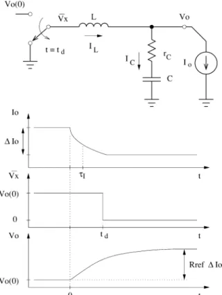
Fig. 7. Buck converter transient response model for a large unloading current step.
unloading step, by a small amount. If tight regulation is re-quired, the output voltage should not overshoot from the speci-fied load-line during large load transients. This requirement con-strains the power filter components. In particular, for a given total (all phase inductors in parallel) inductance value, there is a minimum output capacitance value (critical capacitance) for which this requirement can be met.
The original derivation of the critical capacitance [4], [5] as-sumes that the load-line impedance is equal to the output capac-itor ESR . As discussed in Section II, this design choice is typical for converters using electrolytic output capaci-tors, however, it is not practical with ceramic output capacitors. Here we derive the critical capacitance for a more general output impedance as defined in (1) of Section II. Further, the results presented here incorporate the controller delay and the load cur-rent slew rate, which have not been previously accounted for.
Fig. 7 shows a model of the buck converter response for a large unloading transient. The unloading current step can be modelled by a magnitude and a time constant which characterizes the rise/fall time (or slew rate). The controller is assumed to have a response delay , after which it applies maximum control effort by saturating the duty ratio to zero. Linear-system time constants associated with the controller re-sponse can be incorporated in . Further, the switching node
voltage is modelled as an average value over one switching pe-riod , since the delay effects of the switching action can also be lumped in . Finally, current microprocessor VR specifi-cations allow the output voltage to overshoot by some amount above the defined load-line during unloading transients (see Table I), to reduce the output capacitor requirement [3]. The loading transient can be analyzed analogously. For this model, the critical capacitance required for tight transient load-line support is derived in Appendix B, yielding (31), shown at the bottom of the page, where and
. The above expression yields two values for the crit-ical capacitance—one for the loading, and one for the unloading transient—which typically have different , as shown in (30). The larger value of the two should be used in design. The quan-tity has been identified as a critical inductance value below which the output voltage transient is independent of the induc-tance value [6]–[8]. In [6]–[8], it is suggested that the converter total inductance should be designed to match this critical induc-tance value. This is readily implementable in designs using elec-trolytic capacitors, which have a large ESR time constant. How-ever, it is clear that for capacitor technologies with a small ESR time constant, such as ceramic capacitors, this design choice im-plies impractically small inductance values. The result in (31) presents a consistent framework for transient design with in-ductances above the critical value. They indicate that for de-signs with a small capacitor ESR time constant, where typically , reducing the inductance value is beneficial, from a transient performance perspective, since this decreases the re-quired output capacitance via parameter . These results also show how the converter delay and the load current slew rate af-fect the capacitance choice: larger controller delay and load slew rate require larger output capacitance to handle the transient.
VI. SWITCHING-RIPPLECONSIDERATIONS
The switching-ripple constrains the power train design with regard to both regulation performance and efficiency. The in-ductor current ripple of a single phase has a peak-to-peak am-plitude of
(32) and a frequency of [29, Ch.2]. The inductor current ripple incurs conductive and core losses which may aggravate the con-version efficiency, and limit high-frequency performance [29, Ch.13]. The total inductor current (sum of all inductor currents) ripple of an -phase interleaved buck converter can be shown to be
(33)
for
where 1/N . The total inductor current ripple frequency is . In buck converters with a coupled inductor, the total inductor current ripple is also given by (33), however the phase current ripple is smaller than that in conventional un-coupled implementations [9], [10]. In particular, the phase cur-rent ripple is equal to the total-inductor curcur-rent ripple (33) di-vided by the number of phases
(34) which is always smaller than (32) for a given set of power-train parameters.
The total inductor current ripple (33) results in voltage ripple across the output capacitor and its ESR. The output voltage ripple can be accurately approximated by combining the mag-nitudes of the capacitor and ESR ripples, yielding
(35) Note that expression (35) does not include the ripple contri-bution due to the output capacitor effective series inductance (ESL). The ESL depends strongly on the capacitor packaging and circuit layout [33], [34]. Since the output voltage ripple af-fects the regulation performance, it can be yet another factor constraining the choice of output capacitor. Finally, note that while the interleaved multiphase operation reduces the output voltage ripple (35), it does not affect the inductor current ripple in the individual phases (32), in a conventional, uncoupled in-ductor design.
VII. APPLICATION TOMICROPROCESSORVRS
Load-line regulation is adopted as a standard control method in microprocessor VRs [3]. Hence, the discussion above can be applied directly to the design of VRs.
A. Output Capacitor Size
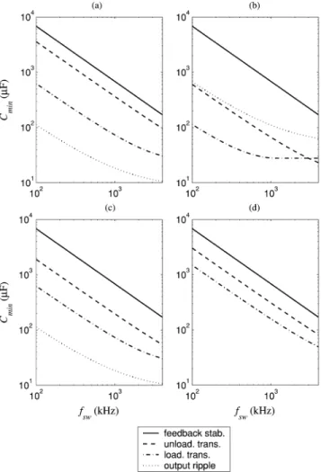
Three important design considerations that impose a lower limit on the VR’s output capacitance were discussed in the pre-vious sections: First, the capacitor size is constrained by feed-back stability requirements as given by (10) and (17). Second, the critical capacitance requirement (31) has to be met for both the loading and unloading transients. Third, the output voltage ripple (35) limits the capacitor choice as well. In Fig. 8, these constraints are plotted versus switching frequency for a number of VR architectures, assuming VR parameters from Table I, and 4 24 ns, 8 A, 16 mV, 100 ns, and 1/6. For these specifications, the phase inductance is calculated from (32) for the VR examples with un-coupled inductors, and from (34) for the un-coupled-inductor design. Fig. 8(a) characterizes a conventional 12 V-input VR topology. Fig. 8(b) presents a coupled-inductor implementation [9], [10] which meets the specified phase current ripple requirement with much smaller total inductance (see Section VI). As a result of the lower total inductance, the loading and unloading transient con-straints on the output capacitance are relaxed, compared to the uncoupled case. However, the lower inductance also yields higher total inductor current ripple, requiring larger capacitance to
main-Fig. 8. Minimum output capacitance constraints versus switching frequency, associated with unloading and loading transient response, feedback stability, and output ripple. (a)V =12 V. (b) Coupled inductors. (c) Synchronous rectifier turned off during unloading. (d)V =5 V. Note: In (d), the output ripple constraint yieldsC <10F which is below the range of the plot.
TABLE I
SAMPLEMICROPROCESSORVR SPECIFICATIONS
tain the specified output voltage ripple. Fig. 8(c) depicts a con-verter with “body braking” which turns off the synchronous recti-fier when the duty-ratio command saturates to zero, forcing
con-duction through the body diode, and thus increasing the voltage across the inductor by a diode drop [11]. In this calculation, it is assumed that 1 V. Fig. 8(d) characterizes the second stage in a two-stage VR topology, powered from an intermediate 5-V bus [12]. Note that in all cases the feedback stability require-ment dominates the other constraints. This is especially true for architectures that are specifically tailored for efficient low-con-version-ratio operation [Fig. 8(b)–(d)]. Importantly, if load-cur-rent feedforward is used, as discussed in Section IV, the feedback stability constraint is removed since ideally there are no stability limitations of the feedforward control path. In such a case, Fig. 8 suggests that the size of the output capacitor can be reduced by factors of at least 2 to 8, depending on the architecture used. Thus, the regulation specification can be met with a small number of multilayer ceramic capacitors (MLCCs) in the range of hundreds of F at sub-MHz switching frequencies.
B. Load-Current Estimation
The load feedforward control strategy discussed in Section IV assumes that the load current is measured. Sensing the load current directly is not practical since it will require inserting a sense resistor in the load current path, thus increasing the output impedance and power loss, or using an expensive Hall-ef-fect current sensor. Alternatively, the load current can be recon-structed from estimates of the inductor and capacitor currents since [1], [6], [15]
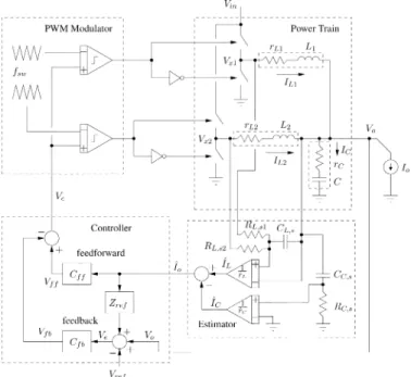
(36) The inductor current can be estimated with an filter con-nected in parallel with the inductor, and having time constant equal to this of the inductor. This “lossless inductor sensing” ap-proach has been used successfully in commercial products [11]. The capacitor current can be estimated in the same way. A VR implementation diagram, using this load current estimation ap-proach and passively summing the inductor current estimates of the different phases [1], [15] is shown in Fig. 9.
In the case of perfect matching of the estimator and power train parameters, the injection of the load current estimate in the controller does not affect the closed-loop poles and zeros of the system. This is due to the fact that and contain the same state information, when the load is a current source, and this state information is subtracted out when the two are combined in (36) yielding the exogenous variable . In practice, there typically is some mismatch between the estimator and power train parameters, resulting in the load current estimate becoming a function of the converter state variables and hence altering the system pole and zero locations. For small mismatches this effect is small, and can be tolerated in a properly designed controller. Finally, other load current estimation approaches can be de-ployed as well. For example, methods involving adaptive param-eter estimation may provide a more accurate and robust load-current estimate.
C. PWM Modulator
A switch modulation scheme having a very low latency is es-sential for achieving a fast controller response with load-current feedforward. Good candidates include unlatched level-sensitive PWM (with some hysteresis for noise immunity), leading-edge
Fig. 9. Implementation diagram of a two-phase buck converter with load-line regulation and estimated load-current feedforward.
latched PWM, two-sided latched PWM [35], and valley cur-rent-mode control [36]. All of these have turn-off latency equal to or less than the steady-state on-pulse-width, which is about a tenth of the switching period in 12 V-input VRs.
D. Dynamic Reference Voltage
In this discussion we have assumed that is constant. In modern microprocessor systems can be adjusted during operation. However, this happens at slow rates compared to changes in the load current (e.g., reference voltage slew rate of 2.2 mV s, [3]), and hence tracking it does not present a substantial challenge. In fact, a simple and effective reference voltage feedforward, providing good tracking up to the cutoff frequency, can be accomplished by directly adding to the input of the PWM modulator.
VIII. SIMULATIONS ANDEXPERIMENTALRESULTS
A. Converter Implementation
To demonstrate the use of load-current feedforward to improve load-line regulation performance, a four-phase ver-sion of the controller structure in Fig. 9 was implemented. A synchronous buck converter board (International Recti-fier IRDCiP2002-C) was modified to incorporate estimated load-current feedforward. The on-board PWM modulator (Intersil ISL6558) uses voltage-mode, latched trailing-edge modulation with phase-current balancing. The converter pa-rameters are summarized in Table II. The feedforward law (24) from Section IV-A was used.
B. Simulations
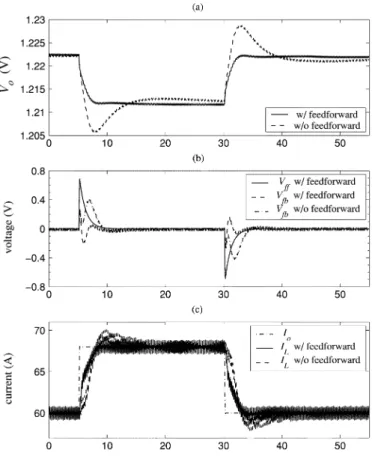
The system was simulated in PSIM (Powersim Inc.). Figs. 10 and 11 show the converter transient response to load steps of dif-ferent magnitude, with and without load-current feedforward. In Fig. 10, a small 8-A load step is depicted. With load-current
TABLE II
EXPERIMENTALCONVERTERPARAMETERS
feedforward the output voltage adheres tightly to the prescribed load-line [Fig. 10(a)]. In Fig. 10(b), it can be seen that the feed-forward path contributes the bulk of the duty-ratio command signal, while the feedback signal has a small magnitude. In con-trast, without load-current feedforward, the control effort is de-termined solely by the feedback path, and the output voltage deviates substantially from the desired load-line. The feedback unity-gain bandwidth is limited to 200 kHz, which is one-fifth of the switching frequency, for the stability reasons discussed in Section III-B. However, according to (9), for the load-line feed-back approach to work successfully, the bandwidth has to be substantially larger than 1/2 153 kHz, which could not be achieved here due to the stability constraint. Clearly, the load-current feedforward circumvents this limitation by pro-ducing a large, fast, exogenous control signal.
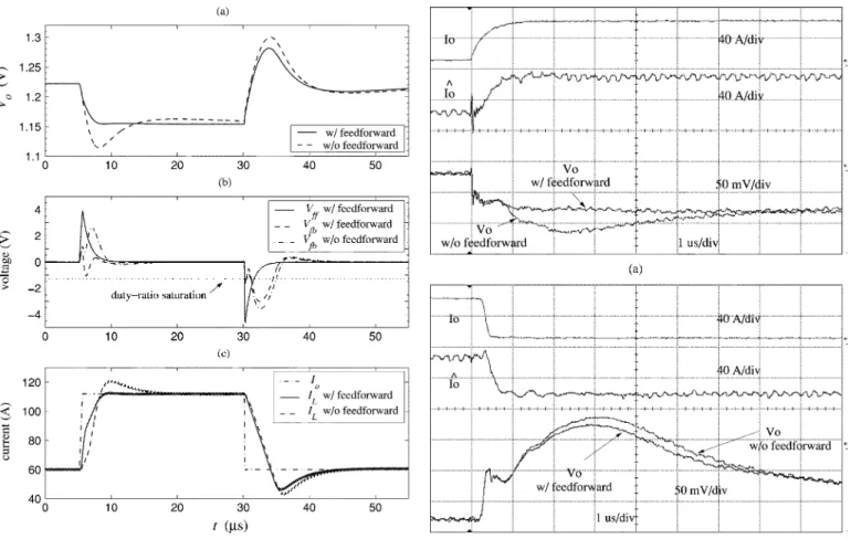
Fig. 11 depicts the converter response to a large 52-A load current transient. The loading transient is a scaled version of the 8-A loading response, since the system has linear average behavior. The unloading step, however, results in duty-ratio sat-uration at zero, due to the low output voltage. The converter be-havior under duty-ratio saturation is consistent with the discus-sion in Section V. Indeed, solving (31) for the unloading voltage overshoot yields 67 mV which matches the simulation. Notice that, compared to pure feedback control, the load-cur-rent feedforward decreases the output voltage overshoot, since it drives the duty ratio to saturation faster.
Fig. 10. Simulated 8-A load transient, from 60 A to 68 A to 60 A, with and without load-current feedforward. (a) Output voltage. (b) Duty ration command (ac component). (c) Load and total inductor current.
C. Hardware Measurements
Fig. 12 shows the experimental prototype transient response, with and without estimated load-current feedforward, for 52-A loading and unloading transients, analogously to Fig. 11. Due to hardware constraints of the pulsed load circuit, the loading rent step has a time constant of about 250 ns. The unloading cur-rent step is much faster, completing the step in less than 200 ns. From the figures it can be seen that the estimated load current follows very well the measured current with a delay of about 100 ns. The 4-MHz switching noise present in the load-current estimate results from parasitic coupling to the sense wires which were soldered on top of the converter board. The switching noise does not affect the dc regulation precision because it is attenu-ated by the PID controller. Further, in a dedicattenu-ated implemen-tation, the sensing can be done through buried, shielded PCB traces, thus reducing both electrostatic and magnetic pickup.
The loading transient in Fig. 12(a) resembles closely the simulation in Fig. 11. With pure feedback control the output voltage sags by 35 mV below the load-line, corresponding to overshoot of more than 50%. On the other hand, load-current feedforward effects tight load-line regulation. The unloading transient in Fig. 12(b) is similar to the one in Fig. 11 as well. The combined feedback and feedforward control produces a slightly better voltage response than the feedback alone, implying a faster transition to duty-ratio saturation. The improvement with feedforward control is not as substantial as that for the loading transient, since the duty-ratio saturation fundamentally limits the performance. An overshoot of about 85 mV is observed,
Fig. 11. Simulated 52-A load transient, from 60 A to 112 A to 60 A, with and without load-current feedforward. (a) Output voltage. (b) Duty ration command (ac component). (c) Load and total inductor current.
which is expected since the duty ratio saturates to zero about 300 ns after the beginning of the step, and (31) predicts over-shoot of 80 mV for these conditions. The transient regulation here can be enhanced if the synchronous rectifier is turned off (body braking), or if a smaller total inductance is used (e.g., with coupled-inductors), as discussed in Section VII-A. Finally, Fig. 13 shows a smaller, 8-A experimental unloading transient which parallels the simulation in Fig. 10 with some additional sensing and measurement noise associated with the prototype. Again, it is clear that the combination of feedback and feedforward provides tighter output impedance regulation than feedback alone.
IX. CONCLUSION
This paper presented a consistent framework for load-line regulation of the buck converter using output capacitors with an arbitrary ESR time constant, encompassing electrolytic and ceramic technologies. In both current-mode and voltage-mode control, load-current feedforward can extend the useful band-width beyond that achievable with pure feedback, since feed-forward is not limited by stability constraints. The load-current feedforward is used to handle the bulk of the regulation action by providing a fast duty-ratio control signal. The feedback is used to compensate for imperfections of the feedforward and to ensure tight dc regulation. With load-current feedforward, the output capacitor size is limited only by large-signal transient and
Fig. 12. Experimental 52-A load transient, with corresponding estimated load current, with and without load-current feedforward. (a) Loading step from 60 to 112 A. (b) Unloading step from 112 to 60 A.
Fig. 13. Experimental 8-A unloading transient, from 68 A to 60 A, with corre-sponding estimated load current, with and without load-current feedforward.
switching-ripple considerations. In particular, for representative ceramic-capacitor VR architectures, the large-signal and ripple constraints are shown to be less restrictive than the stability re-quirement, indicating that the use of load-current feedforward is advantageous in this application. The load current can be esti-mated from the inductor and capacitor voltages with simple networks, or with another lossless sensing method. Different types of PWM modulators can be used as long as they have low latency. The ability of estimated load-current feedforward
to provide tighter load-line regulation than pure feedback con-trol was demonstrated with an experimental 12-to-1.3 V, all-ce-ramic capacitor, multi-phase buck converter. These results point to the feasibility of microprocessor VR implementations using only a small number of ceramic output capacitors.
APPENDIX
A. Bandwidth Requirement for Load-Line Feedback Control
Load-line feedback control was discussed in Section III-B. Here, we derive a feedback-loop bandwidth requirement which guarantees the desired output-impedance regulation with this type of control. Assume a perfectly designed PID controller which provides a 20 dB/dec rolloff of the loop gain
with a unity gain bandwidth of 2
(37) The closed-loop output impedance (8) then becomes
(38) At low frequencies, 0 and , as desired. At high frequencies, the open-loop impedance is dominated by the output capacitor
(39) where is the capacitor ESR time constant. Substituting (39) in (38), expanding to its definition in (1), and rearranging terms, we obtain
(40) Clearly, if , then it must be true that , or, equivalently, .
B. Critical Capacitance Calculation
Fig. 7 shows a model of the VR response for a large unloading transient. The unloading current step can be modeled by a mag-nitude and a time constant which characterizes the slew rate
(41) for 0.
Following the load step at 0, the controller reacts after some delay inherent in a physical implementation (Fig. 7). Before the controller has reacted, for 0 , the inductor current remains approximately at its initial value , since the output voltage practically stays constant. Then, the capacitor current is
(42)
and the capacitor voltage is
(43) where
(44) The output voltage is then
(45) for 0 .
After the delay, the maximum control effort the controller can exert is to saturate the duty ratio to zero. Thus, for , the inductor voltage is
(46) ignoring the load current time constant 0 . These approx-imations are reasonable, since under duty ratio saturation is dominated be the constant . The inductor current is then
(47) Thus, the output voltage is
(48) for , where .
We require that the output voltage does not exceed the load-line specification
(49) Since the maximum voltage value is reached at time , the critical capacitance can be derived from (48), by setting
(50) The time when the maximum voltage value is reached, can be obtained by setting the first derivative of (48) to zero, and solving for
The above equation is transcendental, and thus an analytical so-lution for cannot be derived in general. However, for the case of high slew rate load steps (small ), which are most chal-lenging in practice, the exponential term in (51) has negligible contribution to the solution , and can therefore be ignored. Further, the maximum voltage cannot physically occur before time , thus
for
for (52) where . In the general case, can be obtained by solving (51) numerically.
Combining (48) and (51) to eliminate the exponential term, and substituting for , we obtain an expression for . Inserting the result in (50) and solving for we obtain
(53) Substituting the approximate value of from (52) in the above expression yields
for for
(54) This derivation assumes that the inductor current ripple is small compared to the full load step. A discussion of the effect of large inductor current ripple on transient performance can be found in [37].
Finally, if the output voltage is allowed to overshoot above the defined load-line during large transients, this overshoot can be added on the right-hand side in (49) and (50). This re-sults in a modified critical capacitance value (31) which is less stringent than (54) for 0.
ACKNOWLEDGMENT
The authors wish to thank J. Zhang for laying out the con-troller PCB.
REFERENCES
[1] A. V. Peterchev and S. R. Sanders, “Design of ceramic-capacitor VRM’s with estimated load current feedforward,” in Proc. IEEE Power Electron. Spec. Conf., 2004, pp. 4325–4332.
[2] A. V. Peterchev, “Digital Pulse-Width Modulation Control in Power Electronic Circuits: Theory and Applications,” Ph.D. dissertation, Univ. California, Berkeley, 2005 [Online]. Available: http://www. eecs.berkeley.edu/Pubs/TechRpts/2006/EECS-2006-22.html [3] Voltage Regulator—Down, (VRD) 10.1, Intel Corp., Jul. 2004
[Online]. Available: http://developer.intel.com/design/Pentium4/doc-umentation.htm
[4] R. Redl, B. P. Erisman, and Z. Zansky, “Optimizing the load transient response of the buck converter,” inProc. IEEE Appl. Power Electron. Conf., 1998, vol. 1, pp. 170–176.
[5] R. Redl, “DC/DC converters for microprocessor core power supplies,” inLecture Notes Power Manag., Dec. 1999, [CD ROM].
[6] A. V. Peterchev, J. Xiao, and S. R. Sanders, “Architecture and IC imple-mentation of a digital VRM controller,”IEEE Trans. Power Electron., vol. 18, no. 1-II, pp. 356–364, Jan. 2003.
[7] P.-L. Wong, F. C. Lee, P. Xu, and K. Yao, “Critical inductance in voltage regulator modules,”IEEE Trans. Power Electron., vol. 17, no. 4, pp. 485–492, Jul. 2002.
[8] K. Yao, M. Xu, Y. Meng, and F. C. Lee, “Design considerations for VRM transient response based on the output impedance,”
IEEE Trans. Power Electron., vol. 18, no. 6, pp. 1270–1277, Nov. 2003.
[9] J. Li, C. R. Sullivan, and A. Schultz, “Coupled-inductor design opti-mization for fast-response low-voltage DC—DC converters,” inProc. IEEE Appl. Power Electron. Conf., 2002, vol. 2, pp. 817–823. [10] J. Li, A. Stratakos, A. Schultz, and C. R. Sullivan, “Using coupled
inductors to enhance transient performance of multi-phase buck con-verters,” inProc. IEEE Appl. Power Electron. Conf., 2004, vol. 2, pp. 1289–1293.
[11] XPHASE™ VR 10.0 Control IC, std. IR3081a, International Rectifier Corp., Nov. 2004 [Online]. Available: http://www.irf.com/product-info/datasheets/data/ir3081a.pdf
[12] Y. Ren, M. Xu, K. Yao, Y. Meng, and F. C. Lee, “Two-stage approach for 12-V VR,” IEEE Trans. Power Electron., vol. 19, no. 6, pp. 1498–1506, Nov. 2004.
[13] K. Yao, Y. Meng, and F. C. Lee, “A novel winding coupled buck con-verter for high step-down DC/DC conversion,” inProc. IEEE Power Electron. Spec. Conf., 2002, pp. 651–656.
[14] A. V. Peterchev and S. R. Sanders, “Low conversion ratio VRM de-sign,” inProc. IEEE Power Electron. Spec. Conf., 2002, vol. 4, pp. 1571–1575.
[15] X. Zhang, G. Yao, and A. Q. Huang, “A novel VRM control with direct load current feedback,” inProc. IEEE Appl. Power Electron. Conf., 2004, vol. 1, pp. 267–271.
[16] K. Yao, Y. Ren, and F. C. Lee, “Critical bandwidth for the load transient response of voltage regulator modules,”IEEE Trans. Power Electron., vol. 19, no. 6, pp. 1454–1461, Nov. 2004.
[17] Y. Ren, K. Yao, M. Xu, and F. C. Lee, “Analysis of the power delivery path from the 12-v VR to the microprocessor,”IEEE Trans. Power Electron., vol. 19, no. 6, pp. 1507–1514, Nov. 2004.
[18] Y. Panov and M. Jovanovic´, “Design considerations for 12-V/1.5-V, 50-A voltage regulation modules,”IEEE Trans. Power Electron., vol. 16, no. 6, pp. 776–783, Nov. 2001.
[19] Z. Moussaoui, “Digital vs. analog power control for microprocessor core regulation,” inProc. Darnell Dig. Power Forum, Sep. 2004, [CD ROM].
[20] B. Carroll, “Cost-effective digital control for core power,” inProc. Dar-nell Dig. Power Forum, Sep. 2004, [CD ROM].
[21] H. Deng, A. Q. Huang, and Y. Ma, “Design of a monolithic high fre-quency fast transient buck for portable application,” inProc. IEEE Power Electron. Spec. Conf., 2004, pp. 4448–4452.
[22] J. Abu-Qahouq, H. Mao, and I. Batarseh, “Multiphase voltage-mode hysteretic controlled DC–DC converter with novel current sharing,”
IEEE Trans. Power Electron., vol. 19, no. 6, pp. 1397–1407, Nov. 2004.
[23] C. Varga, “Novel controller for next generation portable CPU power,” inProc. Intel Tech. Symp., Sep. 2004, [CD ROM].
[24] R. Redl and N. O. Sokal, “Near-optimum dynamic regulation of DC-DC converters using feed-forward of output current and input voltage with current-mode control,”IEEE Trans. Power Electron., vol. PE-1, no. 3, pp. 181–192, Jul. 1986.
[25] X. Zhou, P.-L. Wong, P. Xu, F. C. Lee, and A. Q. Huang, “Investigation of candidate VRM topologies for future microprocessors,” IEEE Trans. Power Electron., vol. 15, no. 6, pp. 1172–1182, Nov. 2000.
[26] S. Banerjee and G. C. Verghese, Eds., Nonlinear Phenomena in Power Electronics: Attractors, Bifurcations, Chaos, and Nonlinear Control. New York: IEEE Press, 2001.
[27] I. Deslauriers, N. Avdiu, and B. T. Ooi, “Naturally sampled triangle car-rier PWM bandwidth limit and output spectrum,”IEEE Trans. Power Electron., vol. 20, no. 1, pp. 100–106, Jan. 2005.
[28] Y. Qiu, M. Xu, K. Yao, J. Sun, and F. C. Lee, “The multi-fre-quency small-signal model for buck and multiphase interleaving buck converters,” inProc. IEEE Appl. Power Electron. Conf., 2005, pp. 392–398.
[29] R. W. Erickson and D. Maksimovic´, Fundamentals of Power Elec-tronics, 2nd ed. Norwell, MA: Kluwer, 2001.
[30] G. C. Verghese, C. A. Bruzos, and K. N. Mahabir, “Averaged and sam-pled-data models for current mode control: A reexamination,” inProc. IEEE Power Electron. Spec. Conf., 1989, pp. 484–491.
[31] J.-J. E. Slotine and W. Li, Applied Nonlinear Control. Englewood Cliffs, NJ: Prentice-Hall, 1991.
[32] K. J. Åström and T. Hägglund, PID Controllers: Theory, Design, and Tuning, 2nd ed. Research Triangle Park, NC: Instrum. Soc. Amer., 1995.
[33] C. R. Sullivan and A. M. Kern, “Capacitors with fast current switching require distributed models,” inProc. IEEE Power Electron. Spec. Conf., 2001, vol. 3, pp. 1497–1503.
[34] C. R. Sullivan, Y. Sun, and A. M. Kern, “Improved distributed model for capacitors in high-performance packages,” inProc. IEEE Appl. Power Electron. Conf., 2002, vol. 2, pp. 969–976.
[35] P. Midya and K. Haddad, “Two sided latched pulse width modula-tion control,” inProc. IEEE Power Electron. Spec. Conf., 2000, pp. 628–633.
[36] N. Rossetti and S. R. Sanders, “Valley design techniques outperform peak current mode approach for CPU supplies,” inProc. PCIM Power Electron. Syst., Jul. 2001, [CD ROM].
[37] G. J. Mehas, K. D. Coonley, and C. R. Sullivan, “Converter and inductor design for fast-response microprocessor power delivery,” in
Proc. IEEE Power Electron. Spec. Conf., 2000, vol. 3, pp. 1621–1626. Angel V. Peterchev(S’96–M’05) received the A.B. degree in physics and engineering sciences from Har-vard University, Cambridge, MA, in 1999, and the M.S. and Ph.D. degrees in electrical engineering from the University of California, Berkeley, in 2002 and 2005, respectively.
He is presently a Postdoctoral Research Scientist with the Department of Psychiatry, Columbia Uni-versity, New York, where he works on transcranial magnetic brain stimulation. In the Summer of 2003, he was a Co-op at the Portable Power Systems Group, National Semiconductor Corporation, Santa Clara, CA. From 1997 to 1999, he was a Member of the Rowland Institute at Harvard, where he developed
sci-entific instrumentation. From 1996 to 1998, he was a Student Researcher with the Harvard-Smithsonian Center for Astrophysics. His research interests are in mechanisms, technology, and application paradigms of electromagnetic brain stimulation, pulsed power circuits, and analog and digital control of power con-verters.
Dr. Peterchev received the 1999 Tau Beta Pi Prize from Harvard University and a 2001 Outstanding Student Designer Award from Analog Devices, Inc.
Seth R. Sanders(M’88) received the S.B. degrees in electrical engineering and physics and the S.M. and Ph.D. degrees in electrical engineering from the Massachusetts Institute of Technology, Cambridge, in 1981, 1985, and 1989, respectively.
He was a Design Engineer with Honeywell Test Instruments Division, Denver, CO. Since 1989, he has been on the faculty of the Department of Electrical Engineering and Computer Sciences, Uni-versity of California, Berkeley, where he is presently a Professor. During the 1992–1993 academic year, he was on industrial leave with National Semiconductor, Santa Clara, CA. His research interests are in high frequency power conversion circuits and components, in design and control of electric machine systems, and in non-linear circuit and system theory as related to the power electronics field. He is presently actively supervising research projects in the areas of renewable energy, novel electric machine design, and digital pulse-width modulation strategies and associated IC designs for power conversion applications.
Dr. Sanders received the NSF Young Investigator Award in 1993 and multiple Best Paper Awards from the IEEE Power Electronics and IEEE Industry Appli-cations Societies. He has served as Chair of the IEEE Technical Committee on Computers in Power Electronics, and as a Member-At-Large of the IEEE PELS Adcom.