Please cite this article as: R. Niaraki, M. Nobakht, A Sub-threshold 9T Static Random-access Memory Cell with High Write and Read ability with Bit Interleaving Capability, International Journal of Engineering (IJE), TRANSACTIONS B: Applications Vol. 29, No. 5, (May 2016) 630-636
International Journal of Engineering
J o u r n a l H o m e p a g e : w w w . i j e . i rA Sub-threshold 9T Static Random-access Memory Cell with High Write and Read
Ability with Bit Interleaving Capability
R. Niaraki, M. Nobakht*
Department of Electrical Engineering, University of Guilan, Rasht, Iran
P A P E R I N F O
Paper history:
Received 07 December 2015
Received in revised form 15 February 2016 Accepted 04 March 2016
Keywords: Bit Interleaving Virtual Ground Sub Threshold
Static Random-access Memory Soft Error
A B S T R A C T
This paper proposes a new sub-threshold low power 9T static random-access memory (SRAM) cell compatible with bit interleaving structure in which the effective sizing adjustment of access transistors in write mode is provided by isolating writing and reading paths. In the proposed cell, we consider a weak inverter to make better write mode operation. Moreover applying boosted word line feature decreases write mode failure. An access buffer seperates storage node from read access transistor to improve cell stability and prevent data-related leakage in read operation. Applying virtual ground also reduces the leakage. Furthermore, we design the cell control unit. The simulation results at VDD=0.5V exhibit the effectiveness of our proposed cell compared with other counterparts which are suitable for bit interleaving structure. Comparison results on the proposed cell and 6T cell show our cell improved 70% in write power consumption and 90.45% in read power consumption.
doi: 10.5829/idosi.ije.2016.29.05b.06
1. INTRODUCTION1
In advanced electronic systems and portable devices, memory is one of the most important components. Between all different types of memories, the static random-access memory (SRAM) is high speed and commonly used in electronics equipments. Figure 1 (a) shows the standard 6T SRAM cell. These elements consume too much power and since the market for portable electronic devices is developing extensively, the designers are interested in making memories which consume less power [1]. One of the influential factors in decreasing the power consumption is reducing the cell's
power supply voltage because circuit power
consumption is directly related to power supply voltage used in the cells. The more power supply voltage decreases, the less will be the power consumption.
However as mentioned in the literature [2], along with reduction in power supply voltage, the standard 6T SRAM cell sensitivity increases and correct read operation, correct write operation and the cell stability
1*
Corresponding Author Email: [email protected] (M. Nobakht)
will be endangered. Figure 1 (a), (b), (c) and (d) show different SRAM cells, including standard 6T SRAM, the proposed 7T cell [3], the proposed 12T cell [4] and the proposed 10T cell [5], respectively.
(a) (b)
(c) (d)
New researches lead to design less power consumption SRAM cells for portable low power devices. In the previous researches, different SRAM cells have been proposed to work in low power supply voltage. Different SRAM cells shown in Figure 1 (b-d) have been proposed to work in low power supply voltage with read and write correctly in high stability. The 7T SRAM uses different paths to read and write. Thus the access transistor sizing is not a challenge and read and write operations are done correctly. On the other hand, in the write mode, one of the inverters has been made weaker so that the write operation can be done more strongly. However, this cell experiences data-related leakage in the read path which results in more leakage power consumption. In order to prevent such data leakage and more read stability, various cells have been proposed [4, 5], (Figure 1(c - d)) in which a buffer separates the storage node from the read path. This technique solves data-related leakage problem and on the other hand, causes read stability equal to hold stability.
This paper proposes a new 9T cell, which can work in the sub-threshold region, and has high write ability and good read mode. The proposed cell writes correctly in low supply voltage and is faster compared to other cells comatible with bit interleaving architecture. The proposed cell also is applied to bit interleaving architecture in order to overcome the soft error.
The rest of this paper is organized as follows. Section 2 describes some challenges of standard 6T SRAM cell in sub-threshold region. Then since our proposed 9T SRAM cell is somewhat similar to 7T SRAM cell proposed elsewhere [3], we introduce this cell and explain its different modes. Section 3 analyses the proposed 9T SRAM cell in read mode, write mode and bit interleaving structure. Furthermore, this section provides the circuits to control the proposed cell. The simulation results of the proposed cell and its comparision with other similar cell is presented in section 4. In this section, the data analysis confirms the superiority of the proposed 9T cell. The paper is concluded in section 5.
2. A BRIEF REVIEW ON 6T AND 7T SRAM CELLs
2. 1. 6T SRAM Cell The standard 6T SRAM cell uses two inverters and two NMOS transistors to store the data and access the storage nodes, respectively. Figure 1(a) shows the 6T SRAM cell architecture, including the transistors M1 and M2 as driver transistors, M3 and M4 as load transistors, and M5 and M6 as access transistors. When the VDD decreases, the power consumption fails down and the percentage of incorrect read and write operations increase [3]. In this situation, the 6T stability specially in read mode and cell resistance reduce against soft error [3-5]. Moreover,
read delay and write delay increase. On the other hand, the wrong sizing of 6T SRAM cell cause incorrect read and write operations. In order to have successful reading, access transistor should be small and for successful writing, it must be large. This issue, makes more difficult cell design in sub-threshold region [3, 6].
2. 2. 7T SRAM Cell Sub threshold 7T SRAM cell proposed in the literature [3] is shown in Figure 1 (b). This cell has better performance in sub threshold region compared with 6T SRAM cell. In this cell, read and write operations is improved by separating reading and writing paths and one of the inverters has been weakened. In this cell, transistors M5 and M6 are write and read access transistors, respectively.
2. 2. 1. Reading Operation in 7T Cell In this mode, BLT is precharged to VDD. Then, reading operation will be started through setting RWL to "1". If we assume that Q is equal to "0", by turning on the transistor M6, BLT node capacitor will be decharged through transistors M2 and M6 and the "0" logic will be transmitted to the output. Note that, since reading and writing access transistors are separated, setting the dimensions of accsee transistors can be carried out simply. In this mode, the size of reading access transistor, (M6), can be chosen as small as possible rather than the driver transistor, (M2), in order to have a more successful reading operation.
2. 2. 2. Writing Operation in 7T Cell In writing mode, new data is placed on port BLC. Then, writing operation will be started through setting WL to "1". The writing operation is conducted simply through turning on the writing access transistor, (M5), and turning off the transistor M7 by WL. Assume that node QB has logic value "1", after turning off transistor M7, transistor M3 is degraded and the maintenance capability of the cell will be decreased. Under this condition, the existing data at BLC port will be simply transmitted to the QB node by writing access transistor M5. If node QB is in "0" logic value, transistor M1 must be weakened. This task is done by virtual ground. Indeed, the virtual ground is floated in the writing mode, resulting in degradation of transistor M1 and it takes the "0" logic value in both holding and writing modes in order to maintain the saved data in the cell. In this mode, due to the separation of writing path from the reading one, decision on dimensions of writing access transistor is carried out easily. Indeed, this transistor can be designed as large as possible to have a better writing performance.
increase in power consumption of the cell (at times in which this path is not utilized). However the stability of 7T cell is better than 6T because of the separated reading and writing paths, this cell still suffers from low stability conditions in reading mode. Whereas in a good SRAM design the same reading and holding mode stability is a target.
3. THE PROPOSED 9T SRAM CELL
The proposed 9T SRAM cell is presented in Figure 2. This cell uses two different paths to read and write operations. To have correct read and write operations, boosted word line feature (VDD + 0.1V) is applied. Read part shown in right hand side dashed line is responsible for read operation. In this mode, the transistor M7 separates the storage node from the transistor M8. Using this technique, the static noise margin of read mode is equal to the static noise margin of hold mode. On the other hand, the cell gets free of the data-related leakage. Write part on the left hand side of the cell operates as write mode. The central part of the cell contains the holding core.
3. 1. Read Operation In Figure 2, suppose that node QB has a logic "0" value. In the read mode, RBL is pre-charged to VDD value. The read word line (RWL) receives VDD + 0.1V value and virtual ground (VG) is connected to GND. After M8 is turned on, the read operation happens and Q is moved to RBL. Now suppose that the logic "1" is stored in node QB. In this case, M7 turns on and RBL capacitor is discharged by M7 and M8, which moves "0" to RBL.
3. 2.Write Operation Suppose we want to write "0" in the proposed 9T SRAM cell in Q node. To do so, the "0" placed on WBL and the write word line (WWL) receives the value (VDD + 0.1V) and WWLB receives "0". In these conditions, M5 and M6 are turned off and the internal feedback of inverter becomes weaker. Also, M9 is turned on and "0" is transferred successfully by transistor M9 to be stored in node Q. The write operation of "1" is similar to "0". To write data VG is connect to VDD in order to reduce the cell leakage and lower the power consumption. Table 1 shows different node values of 9T SRAM cell in different modes. In reading and writing modes, we have utilized "VDD+0.1V", thus reading and writing delay would be decreased and read and write operations are carried out in more speed. Thus, in boosted word line, write failure is decreased and write margin is increased.
3. 3. Proposed 9T Cell in Bit Interleaving Structur There are two sensitive nodes to store data in the SRAM cell, called Q and QB.
Figure 2. Proposed 9T SRAM cell
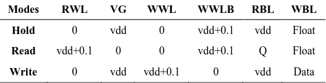
TABLE 1. The values of nodes for the proposed cell in
different modes (V)
Modes RWL VG WWL WWLB RBL WBL
Hold 0 vdd 0 vdd+0.1 vdd Float
Read vdd+0.1 0 0 vdd+0.1 Q Float
Write 0 vdd vdd+0.1 0 vdd Data
In a good design, the electrical charge of node capacitors have to be more than the critical charge. The critical charge is the minimum charge needed for changing the capacitor status [6-9], from its correct value. Some particles including the low-energy neutrons [10, 11], high-energy neutrons and the alpha particles [10, 12] are able to create unwanted flips from "1" to "0" or "0" to "1" and cause soft error in SRAM cells. Complex error-correcting techniques in memories can increase reliability in this situations.
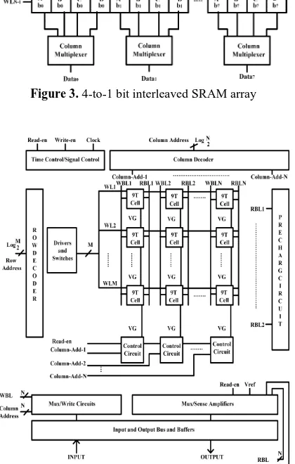
Another effective way to overcome the soft error is to implement a SRAM bit-cell with bit interleaving structure. Figure 3 shows a 4-to-1 bit interleaved SRAM array. In each row, bit-cells of words A, B, C and D are interleaved and share one word line. These words have 8-bits. As it can be seen, in this structure, bit 0 (b0) of words A, B, C and D are put together, also bit 1 (b1) of the words are put together and so on. During a read and write operation, the column multiplexers select the bit lines of accessed columns among words A, B, C and D. Cells designed with bit interleaving structure, use simple designs for error correction. The proposed cell can be applied to the bit interleaving architecture. Therefore, it is possible with single-bit error correction techniques to modify the soft error occurred in several cells.
Figure 3. 4-to-1 bit interleaved SRAM array
Figure 4. The full architecture of the proposed SRAM
Figure 5. The control circuit of the proposed cell with
dynamic VDD
Figure 6. The control circuit of the proposed cell with
constant VDD
As shown in this figure, in each column, one control circuit is enough. In read and write operations, if the corresponding column is selected, necessary elements are connected by corresponding control circuit and the read and write cell is done in the selected column.
The control circuits of the proposed cell are presented in Figures 5 and 6. The control circuit in Figures 5 is designed based on the hypothesis that the cell will use the dynamic power supply. Two values of VDD1 and VDD2 are used where the former is smaller than the latter. When the cell is in the hold and write modes, the proposed cell power supply is connected via this control circuit to VDD1=0.2V and VG connects to HIGH value. When the cell is in read mode, the power supply connects to VDD2=0.39V and VG connects to LOW value. The control circuit of Figure 6 is designed with the idea that the cell has constant VDD. Thus, just VG have to be controlled.
4. SIMULATION RESULTS
We simulated proposed 9T SRAM cell in 32nm PTM technology. In the simulation, stability, power consumption and delay of our proposed 9T cell was compared to other cells capable of being applied to the bit interleaving architecture and to the standard 6T SRAM as well.
4. 1.Write Margin and SNM In order to analysis the write ability in the SRAM cell, we used write margin (WM) parameter. To measure the write margin (WM) of different cells, the second method [13] is considered. The WM of different cells versus supply voltage, is shown in Figure 7. We examined 1000 MONTE CARLO simulations to model the variability in SNFP corner and at the temperature of 25°C. The corresponding parameters are gate-oxide thickness and channel length, while the distribution type is the Gaussian with sigma equal to 3.
In the proposed cell, owing to boosted write word line feature and weak internal feedback in the cell during write operation, write operation is more likely to succeed.
Larger WM of the proposed cell in Figure 7 confirms this prediction. Figure 8 shows the effect of temperature deviations on WM. This simulation, at SNFP corner and constant supply of 0.5V is conducted through sweeping the temperature from -40 to 75 degrees.
Figure 7. WM of different cells versus supply voltage in SNFP corner and in the presence of process variation
Figure 8. The effect of temperature deviations on WM
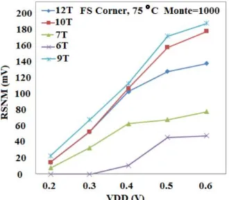
Figure 9.HSNM of different cells versus supply voltage
Figure 10. RSNM of different cells versus supply voltage
Figure 11. RSNM temperature variations of the proposed cell
To find the SNM of circuits we plot the butterfly diagram of them and try to put a square with maximum dimension in the plot. Value of this square leg is equal to SNM [14]. Figures 9 and 10 show HSNM and RSNM of different cells, respectively. We have run Monte Carlo simulations with 1000 iterations in order to model the deviations in FS corner and at 75°C.
The corresponding parameters are gate-oxide thickness and channel length. The distribution type is Gaussian with sigma equal to 3. Since the proposed cell uses separate read and write paths and the storage node is separated from the read access transistor by buffer, the RSNM of the cell is equal to its HSNM. Figure 11 shows RSNM temperature variations of the proposed cell in TT corner.
Figure 12. Write power consumption of various cells versus supply voltage
Figure 13. Read power consumption of various cells versus supply voltage
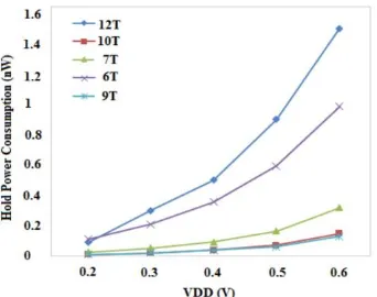
Figure 14. Hold power consumption of various cells versus
supply voltage
4. 3. Write and Read Delays Figure 15 shows the write time delay (WTD) and read time delay (RTD) for various cells in VDD=0.5V. In order to compute the WTD, the cells examine in the write mode and then the time difference from the 50% of the write word line and hitting of the Q and QB signals is computed. The resulting value is called the WTD and its reverse is
called write speed. RTD is defined as the time between the read word line, is set to "1" and the time in which 50 mV voltage difference occurs between bit line and its complement (or between read bit-line and VDD rail in cells with single ended read operation). RTD reverse is called read speed. As it can be seen, WTD for the proposed cell and the 10T cell is 1ns which is less than the WTD for other cells.
Figure 15. WTD and RTD of various cells in VDD =0.5V
5. CONCLUSION
In this paper, a new bit interleaving 9T SRAM cell with different paths, the boosted voltage to read and write word line (VDD + 0.1 V) and weak internal feedback during write operation is presented that improves write-ability compared with conventional 6T SRAM cell. To improve the reading operation, an access buffer is used that separates storage node from read access transistor. Also, to reduce leakage, the virtual ground is used and its control circuits are presented. The proposed 9T SRAM cell performs effectively, write operations with high speed and in supply voltage 0.2V. Also, supply voltage in reading mode is 0.39V. Simulation results in a PTM 32 nm technology show that the proposed design improves power consumption compared with other cells. Furthermore, the proposed cell in comparison with similar SRAM cells, which are compatible with bit interleaving structure has better performance in write and read modes.
6. REFERENCES
1. Do, A. T., Yeo, K. S., Low, J. Y. S., Low, J. Y. L. and Kong, Z. H., "An 8t sram cell with column-based dynamic supply voltage for bit-interleaving", in Circuits and Systems (APCCAS), IEEE Asia Pacific Conference on, (2010), 704-707.
2. Khayatzadeh, M. and Lian, Y., "Average-8t differential-sensing subthreshold sram with bit interleaving and 1k bits per bitline",
Very Large Scale Integration (VLSI) Systems, IEEE Transactions on, Vol. 22, No. 5, (2014), 971-982.
4. Chiu, Y.-W., Hu, Y.-H., Tu, M.-H., Zhao, J.-K., Chu, Y.-H., Jou, S.-J. and Chuang, C.-T., "40 nm bit-interleaving 12t subthreshold sram with data-aware write-assist", Circuits and Systems I: Regular Papers, IEEE Transactions on, Vol. 61, No. 9, (2014), 2578-2585.
5. Chang, I. J., Kim, J.-J., Park, S. P. and Roy, K., "A 32 kb 10t sub-threshold sram array with bit-interleaving and differential read scheme in 90 nm CMOS", Solid-State Circuits, IEEE Journal of, Vol. 44, No. 2, (2009), 650-658.
6. Bota, S. A., Torrens, G., Verd, J. and Segura, J., "Detailed 8-transistor sram cell analysis for improved alpha particle radiation hardening in nanometer technologies", Solid-State Electronics, Vol. 111, (2015), 104-110.
7. Alorda, B., Torrens, G., Bota, S. and Segura, J., "Adaptive static and dynamic noise margin improvement in minimum-sized 6t-sram cells", Microelectronics Reliability, Vol. 54, No. 11, (2014), 2613-2620.
8. Rosa, F., Brum, R., Wirth, G., Kastensmidt, F., Ost, L. and Reis, R., "Impact of dynamic voltage scaling and thermal factors on sram reliability", Microelectronics Reliability, Vol. 55, No. 9, (2015), 1486-1490.
9. Torrens, G., Alorda, B., Barcelo, S., Rossello, J. L., Bota, S. A. and Segura, J., "Design hardening of nanometer srams through
transistor width modulation and multi-vt combination", Circuits and Systems II: Express Briefs, IEEE Transactions on, Vol. 57, No. 4, (2010), 280-284.
10. Baumann, R.C., "Radiation-induced soft errors in advanced semiconductor technologies", Device and Materials Reliability, IEEE Transactions on, Vol. 5, No. 3, (2005), 305-316. 11. Ibe, E., Taniguchi, H., Yahagi, Y., Shimbo, K.-i. and Toba, T.,
"Impact of scaling on neutron-induced soft error in srams from a 250 nm to a 22 nm design rule", Electron Devices, IEEE Transactions on, Vol. 57, No. 7, (2010), 1527-1538.
12. Sil, A., Bakkamanthala, S., Karlapudi, S. and Bayoumi, M., "Highly stable, dual-port, sub-threshold 7t sram cell for ultra-low power application", in New Circuits and Systems Conference (NEWCAS), IEEE 10th International, (2012), 493-496.
13. Wang, J., Nalam, S. and Calhoun, B. H., "Analyzing static and dynamic write margin for nanometer srams", in Low Power Electronics and Design (ISLPED), ACM/IEEE International Symposium on, IEEE, (2008), 129-134.
14. Mostafa, H., Anis, M. and Elmasry, M., "Adaptive body bias for reducing the impacts of nbti and process variations on 6t sram cells", Circuits and Systems I: Regular Papers, IEEE Transactions on, Vol. 58, No. 12, (2011), 2859-2871.
A Sub-threshold 9T Static Random-access Memory Cell with High Write and Read
Ability with Bit Interleaving Capability
R. Niaraki, M. Nobakht
Department of Electrical Engineering, University of Guilan, Rasht, Iran
P A P E R I N F O
Paper history:
Received 07 December 2015
Received in revised form 15 February 2016 Accepted 04 March 2016
Keywords: Bit Interleaving Virtual Ground Sub Threshold
Static Random-access Memory Soft Error
ديكچ ه
ٍئاسا ٍب ٍلاقم هیا ٍظفاح لًلس کی ی
ذیذج یکیتاتسا ی 9
یم یسًتسیضواشت تیب ساتخاس اب ساگصاس لًلس هیا .دصادشپ
ي نذواًخ یاَشیسم یصاساذج اب ،هتشًو ذم سد یسشتسد یاَسًتسیضواشت شثًم داعبا میظىت نآ سد ٍک تسا گىیًیلشتىیا
مَاشف هتشًو یم شظو سد فیعض اس اَشتسًىیا صا یکی ،هتشًو ذم سد دشکلمع دًبُب یاشب یداُىشیپ لًلس سد .تسا ٌذش
-ٍب اب هیىچمَ .میشیگ ٍملک طخ یگژیي هتفشگ ساک
یم شَاک هتشًو ذم سد یباشخ خشو ،ٌذش تیًقت ی شواًخ شیسم سد .ذبای
تسباي یتشو صا یشیگًلج ي ذم هیا یساذیاپ دشکلمع دًبُب یاشب ٌشگ یسشتسد شفاب ،ٌداد ٍب ٍ
یاَسًتسیضواشت صا اس ٌشیخر ی
یم اذج شواًخ یسشتسد ذىک
. ٍب یم یتشو شَاک ثعاب ضیو یصاجم هیمص یشیگ ساک لًلس یاشب ضیو لشتىک ذحاي ساذم .دًش
یصاس ٍیبش جیاتو .تسا ٌذش یحاشط
اَ
ٍیزغت سد
ی
5 / 0 ناشو ،تلي
یم
لًلس اب ٍسیاقم سد یداُىشیپ حشط ٍک ذَد
اَ
ی
لًلس ي ٌذش داُىشیپ لًلس هیب ٍسیاقم جیاتو .دساد یشتُب دشکلمع ذىتسَ گىیًیلشتىیا تیب ساتخاس اب ٍک یشگید 6
ناشو ،دساذواتسا یسًتسیضواشت
یم
اس هتشًو ذم ناًت فشصم یداُىشیپ حشط ٍک ذَد 70
اس شواًخ ذم ناًت فشصم ي ذصسد
55 / 90 دًبُب ذصسد
یم
.ذشخب
![Figure 1. Different cells, (a) the standard 6T SRAM cell, (b) the proposed 7T cell [3], (c) the proposed 12T cell [4] and (d) the proposed 10T cell [5]](https://thumb-us.123doks.com/thumbv2/123dok_us/217581.2016243/1.595.312.539.498.679/figure-different-cells-standard-sram-proposed-proposed-proposed.webp)