R E V I E W
Open Access
Interface engineering for high performance
graphene electronic devices
Dae Yool Jung
†, Sang Yoon Yang
†, Hamin Park, Woo Cheol Shin, Joong Gun Oh, Byung Jin Cho
*and Sung-Yool Choi
*Abstract
A decade after the discovery of graphene flakes, exfoliated from graphite, we have now secured large scale and
high quality graphene film growth technology via a chemical vapor deposition (CVD) method. With the
establishment of mass production of graphene using CVD, practical applications of graphene to electronic devices
have gained an enormous amount of attention. However, several issues arise from the interfaces of graphene
systems, such as damage/unintentional doping of graphene by the transfer process, the substrate effects on
graphene, and poor dielectric formation on graphene due to its inert features, which result in degradation of both
electrical performance and reliability in actual devices. The present paper provides a comprehensive review of the
recent approaches to resolve these issues by interface engineering of graphene for high performance electronic
devices. We deal with each interface that is encountered during the fabrication steps of graphene devices, from the
graphene/metal growth substrate to graphene/high-k dielectrics, including the intermediate graphene/target substrate.
Keywords:
Graphene; Interface engineering; Transfer; Delamination; Mobility; Doping; Hysteresis; Substrate effect;
Dielectric; Transistor
1 Introduction
Graphene has received massive attention as a promising
new material for application to electronic and
optotronic devices because of its superior and unique
elec-trical, optical, and mechanical properties [1-10]. In the
early stage of graphene research, high quality graphene
obtained by mechanical exfoliation [1-8] of graphite
fa-cilitated fundamental studies on the outstanding
proper-ties of graphene, triggering explosive research on the
application of graphene to various fields [11-15].
How-ever, the application of graphene to real-world devices
requires a scalable synthesis technique to overcome the
limited quantity and size of mechanically exfoliated
gra-phene. Graphene synthesis by chemical vapor
depos-ition (CVD) [16-25] is currently the most widely
adopted technique for the scalable production of single
layer graphene, up to a size of 30 inches [19]. Although
large-scale, high-quality graphene is now available, the
realization of high performance graphene devices is still
challenging. Specifically, devices fabricated from
CVD-grown graphene have not yet shown the level of
per-formance that was anticipated upon the emergence of
graphene [26-29]. While the degradation of the
per-formance of graphene devices can be attributed to many
factors, the significant issue of the interfaces where
gra-phene interacts with the neighboring materials warrants
extensive consideration [30-35]. Due to the
one-atom-thick, two-dimensional (2D) characteristic of graphene,
its electrical properties are directly affected by the
inter-action of the graphene surface with adjacent materials.
The purpose of this review is to shed light on the
im-portance of interface engineering through the entire
fab-rication process of graphene devices from several recent
reports on graphene transfer and graphene electronic
devices. In this review, we start from novel transfer
tech-niques via direct delamination of graphene from a metal
growth substrate, which is closely relevant to the
inter-face control in a graphene/growth (or graphene/target)
substrate. After the transfer process, graphene forms an
interface with a target substrate, which also influences
* Correspondence:[email protected];[email protected]†Equal contributors
Graphene Research Center, Department of Electrical Engineering, Korea Advanced Institute of Science and Technology (KAIST), Daejeon 305-701, Republic of Korea
© 2015 Jung et al.; licensee Springer. This is an Open Access article distributed under the terms of the Creative Commons Attribution License (http://creativecommons.org/licenses/by/4.0), which permits unrestricted use, distribution, and reproduction in any medium, provided the original work is properly cited.
the charge carrier transport of graphene. Hence, we
dis-cuss the substrate effects and the choice of an optimum
substrate for high performance graphene devices. Finally,
when graphene is transferred intact onto the target
sub-strate, it is necessary to consider other interfaces that
are created by the integration of graphene with other
electronic components such as gate dielectrics. These
in-terfaces also give rise to challenging issues related to the
chemical inertness of the graphene surface and the
wet-tability/interfacial adhesion. The last topic covers novel
strategies to integrate uniform, ultrathin gate dielectrics
on the graphene surface to guarantee high performance
of graphene devices.
2 Review
2.1 Transfer techniques: interfaces at graphene/metal
growth substrate and graphene/target substrate
Since large-area graphene films are mainly synthesized
on catalytic metal substrates [16-23], we first should
consider the interface between graphene and the
cata-lytic metal substrate. To apply CVD-grown graphene to
electronic devices, graphene must be isolated from this
interface and delivered to a target dielectric substrate.
The most common method for graphene transfer has
been poly(methyl methacrylate) (PMMA) film-assisted
transfer [36-39], which involves wet etching of the metal
substrate and water-mediated delivery of graphene to
the target substrate. Drawbacks of this method include
possible oxidation of graphene due to the strong
oxida-tion power of metal etchants [19] and contaminaoxida-tion of
graphene by etching residues such as ionic impurities
from the etchant [40-42] and metallic residues from
in-complete etching [41]. In addition, polymeric residues
[31-33] after PMMA removal are another source of
con-tamination of graphene. These residues directly affect
the electrical properties of graphene, resulting in
signifi-cant degradation of the performance of graphene devices
[31-33,43]. For these reasons, metal-etching-free transfer
by delamination of graphene from the metal substrate
has been pursued as an alternative, non-destructive
means of realizing clean transfer of graphene.
2.1.1 Electrochemical delamination/transfer of graphene:
physical weakening of the graphene/metal interface
One strategy for direct delamination of graphene is physical
weakening of the interfacial interactions between graphene
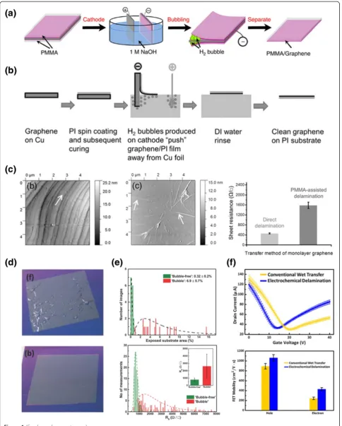
and the metal growth substrate. Figure 1a schematically
il-lustrates the electrochemical delamination (ECD) of
gra-phene in which hydrogen (H
2) bubbles generated by the
electrolysis of water are utilized as a tool for physical
weak-ening of the graphene/metal interface [44]. The
electro-chemical cell employed for the delamination consists of a
PMMA/graphene/metal substrate (cathode, biased
nega-tively) and glassy carbon or noble metal with low reactivity
(anode, biased positively), which are placed in an aqueous
electrolyte solution, such as K
2S
2O
8[44], NaOH [45,46],
Na
2SO
4[47] or NaCl [48,49]. Under applied bias,
electroly-sis of water at the cathode induces the generation and
penetration of H
2bubbles along the interface between
PMMA/graphene and the metal substrate, resulting in
gradual separation of PMMA/graphene from the metal
substrate. Note that partial etching of a copper (Cu) or
nickel substrate can occur by the electrolyte during the
ECD process, and this can be suppressed by the choice of
an appropriate electrolyte such as Na
2SO
4[47]. This
method is highly useful for systems where graphene is
syn-thesized on chemically inert, noble metals such as platinum
[46], ruthenium [50] or iridium [51], because etchants for
corresponding metals are rarely available. Wang et al.
re-ported the application of the ECD process for the direct
transfer of graphene to a flexible polyimide substrate by
de-positing the target polyimide substrate directly onto the
graphene/metal growth substrate, instead of PMMA, where
no water-mediated graphene delivery to a foreign target
substrate is required (Figure 1b) [47]. Elimination of the
conventional use of a sacrificial PMMA enables the
produc-tion of nearly residue-free graphene with a low density line
defects (ripples and wrinkles), yielding flexible, transparent
conducting films with low sheet resistance (~459
Ω
/sq for
single layer graphene, ~49
Ω
/sq for multilayer graphene)
(Figure 1c).
In the ECD based transfer method, one critical issue is
mechanical damage of graphene by H
2bubbles. These
(See figure on previous page.)Figure 1Electrochemical delamination of graphene. a, Illustration of electrochemical delamination of graphene from Pt foil with PMMA sacrificial layer. Reproduced with permission [46]. Copyright 2012, Nature Publishing Group.b, Illustration of direct delamination of graphene onto polyimide substrate without PMMA sacrificial layer. Reproduced with permission [47]. Copyright 2014, John Wiley and Sons.c, AFM images of transferred graphene on polyimide without sacrificial layer (left) and with PMMA sacrificial layer (middle) via electrochemical delamination. Sheet resistance of monolayer graphene on polyimide transferred by the direct delamination method and the PMMA-assisted delamination method (right). Reproduced with permission [47]. Copyright 2014, John Wiley and Sons.d,‘Bubble’(top) and‘bubble-free’(bottom) delaminated and transferred PMMA/graphene stack on oxidized silicon wafer. Reproduced with permission [48]. Copyright 2014, John Wiley and Sons.e, Histograms of percentage of exposed substrate area (top panel) and sheet resistance (bottom panel) for films delaminated using the‘bubble-free’(green) and‘bubble’(red) methods. Inset of bottom panel: Sheet resistance of samples obtained via‘bubble-free’and‘bubble’delamination. Reproduced with permission [48]. Copyright 2014, John Wiley and Sons.f, Transfer characteristics (Id-Vg) of fabricated graphene FET (top panel) and FET mobility (bottom panel) of which graphene are transferred via‘conventional wet transfer’(yellow) process and‘electrochemical delamination’(blue) process.
bubbles can directly damage graphene during the
delam-ination process by considerable turbulence or can result
in cracks (or voids), ripples, and wrinkles due to the
trapped H
2between the graphene and the target
sub-strate (upper panel in Figure 1d) [45,48]. Such
transfer-induced damage or defects severely degrade the
elec-trical properties of graphene devices in terms of mobility
and sheet resistance. To eliminate or reduce the
mech-anical damage caused by H
2bubbles, Cherian et al.
de-veloped a
‘
bubble-free
’
delamination/transfer method by
exploiting the electrochemical reduction (dissolution) of
adventitious cuprous oxide (Cu
2O) sandwiched between
graphene and a Cu substrate as a tool for weakening of
that interface [48]. Reduction of interfacial Cu
2O
oc-curred at an optimum potential lower than that required
for the generation of H
2bubbles. This method resulted
in uniform adherence of PMMA/graphene to the target
substrate (lower panel of Figure 1d) and the resulting
transferred graphene film exhibited a negligible amount
of voids (upper panel of Figure 1e) and high uniformity
of electrical properties (lower panel of Figure 1e).
Dam-ages in graphene by the generation of H
2bubbles can be
also alleviated with a simple plastic-frame-assisted
method [45]. In a previous study we performed
ECD-graphene transfer using a similar method to the
plastic-frame-assisted approach to compare the quality
of the transferred graphene by the ECD method with
that by the conventional PMMA-assisted wet method
in terms of the characteristics of a field-effect
transis-tor (FET). Experimental details are described in [52].
We found that the electrical characteristics of
ECD-graphene FETs reflected the effective suppression of
p-doping (reduced Dirac point) and enhanced FET mobility
with symmetrical electron
–
hole conduction (Figure 1f).
2.1.2 Dry transfer of graphene: difference of adhesion
energy between graphene/metal and graphene/target
substrate interfaces
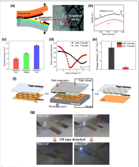
Graphene transfer based on direct delamination can also be
achieved by exploiting the difference in adhesion energies
between graphene/metal and graphene/target substrate
interfaces [53,54]. The basic concept of this approach is
il-lustrated in Figure 2a: An adhesive interface is formed
be-tween a graphene/metal substrate and a target substrate,
and then the two substrates are separated under tensile
loading by double cantilever beam fracture testing [53].
The Raman spectra in Figure 2b indicate that
applica-tion of an appropriate adhesive layer enables
mechan-ical delamination of graphene from the Cu substrate. As
shown in Figure 2c, Shin et al. measured the adhesion
energy of graphene to various adhesive layers (or target
substrates) and found that a graphene/poly(vinyl
phe-nol) (PVP) system exhibited the highest adhesion energy
(2.31 ± 0.11
Jm
−2), higher than that of a graphene/Cu
system (0.72 ± 0.07
Jm
−2) [53]. This indicates that PVP
can act as an appropriate adhesive that induces
success-ful delamination and transfer of graphene from Cu to a
target substrate [54]. Because a wet process is excluded,
this transfer method is called
‘
dry transfer
’
. As
men-tioned in Section 2.1, advantages of the delamination/
transfer method include the restoration of charge
neu-trality and symmetrical electron
–
hole conduction of
graphene, which are usually degraded by a metal etching
process in the conventional wet transfer approach.
Figures 2d and 2e show p-doping suppression and
en-hanced electron current modulation of dry-transferred
graphene FETs, in comparison to graphene FETs
pre-pared using either conventional wet transfer or ECD
transfer (Figure 1f ) [54]. These enhancements obtained
with dry transfer are attributed to the absence of
oppor-tunity for graphene to be contaminated by ionic
impur-ities (from either the electrolyte or metal etchant) and
metallic residues (from incomplete etching of the
metal substrate).
Jung et al. recently exploited a mechano-electro-thermal
(MET) process to induce delamination and dry transfer of
graphene from a Cu substrate directly to various
sub-strates such as glass, PET, and PDMS (Figure 2f ) [55].
The key aspect of this method is to form strong and
ultra-conformal contact between graphene/Cu and a
target substrate by applying high temperature, physical
pressure, and high voltage simultaneously to the Cu
(See figure on previous page.)Figure 2Dry transfer using difference of adhesion energy between graphene/metal and graphene/target substrate. a, Illustration of graphene transfer using the mechanical delamination process and high-magnification SEM image of boundary of delamination. Reproduced with permission [53]. Copyright 2012, American Chemical Society.b, Raman spectra of the graphene-delaminated bare copper (the lower spectrum) and of the graphene-covered copper (the upper spectrum). Reproduced with permission [53]. Copyright 2012, American Chemical Society.c, Directly measured adhesion energy of graphene to neighboring materials (SiO2, PVP, and PMMA). Reproduced with permission [54]. Copyright 2013, AIP Publishing LLC. d, Transfer characteristics (IDS-VGS) of the graphene FETs fabricated using conventional wet transfer (black) method and dry transfer with PVP adhesive layer (red). Reproduced with permission [54]. Copyright 2013, AIP Publishing LLC.e, Charge density of the graphene FETs fabricated using conventional wet transfer (black) method and dry transfer with PVP adhesive layer (red). Reproduced with permission [54]. Copyright 2013, AIP Publishing LLC. f, Schematic description of the mechano-electro-thermal (MET) delamination process of graphene. Reproduced with permission [55]. Copyright 2014, John Wiley and Sons.g, Strong mechanical stability of MET graphene via demonstration of LED electrical circuit based on graphene/PET film using repeated detaching of 3M tape. Reproduced with permission [55]. Copyright 2014, John Wiley and Sons.
foil/graphene/target
substrate
stack.
Graphene
is
transferred to the target substrate simply by peeling the
Cu foil off after the MET process. No polymeric carriers
or adhesives are used in this approach. Most importantly,
graphene transferred by the MET process exhibited
out-standing interfacial adhesion with the target substrate as a
result of the ultra-conformal contact formation: the
mech-anical adhesion stability of graphene is maintained even
after several cycles of tape detaching tests, as shown in
Figure 2g.
2.1.3 Direct delamination/transfer of graphene with high
degree of freedom
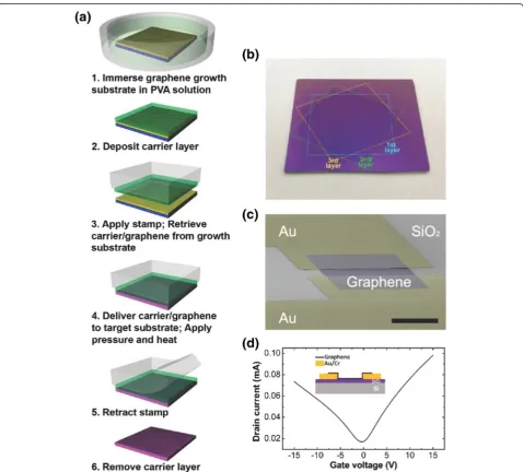
Recently, Yang et al. reported that the combination of
pre-treatment of graphene/Cu substrate with the well-known
transfer printing technique allows clean delamination and
transfer of graphene, which can also endow the graphene
transfer process with a high degree of freedom (Figure 3a)
[56]. Delamination of graphene is induced by the
adsorp-tion of a water soluble polymer (poly(vinyl alcohol) in this
case) on the graphene growth substrate, followed by the
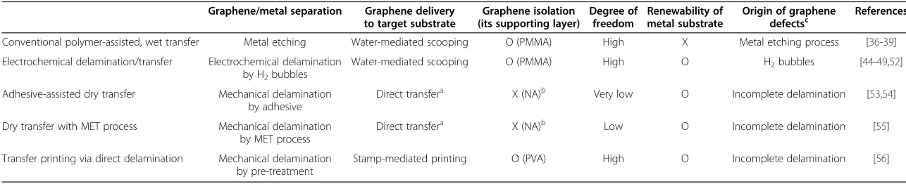
Table 1 Summary of graphene transfer methods
Graphene/metal separation Graphene delivery to target substrate
Graphene isolation (its supporting layer)
Degree of freedom
Renewability of metal substrate
Origin of graphene defectsc
References
Conventional polymer-assisted, wet transfer Metal etching Water-mediated scooping O (PMMA) High X Metal etching process [36-39]
Electrochemical delamination/transfer Electrochemical delamination by H2bubbles
Water-mediated scooping O (PMMA) High O H2bubbles [44-49,52]
Adhesive-assisted dry transfer Mechanical delamination by adhesive
Direct transfera X (NA)b Very low O Incomplete delamination [53,54]
Dry transfer with MET process Mechanical delamination by MET process
Direct transfera X (NA)b Low O Incomplete delamination [55]
Transfer printing via direct delamination Mechanical delamination by pre-treatment
Stamp-mediated printing O (PVA) High O Incomplete delamination [56]
a
Delamination and transfer of graphene occur simultaneously.b
Supporting layer is not applicable.c
Defects include damage or contamination of transferred graphene.
Jung
et
al.
Nano
Converg
ence
(2015) 2:11
Page
7
of
formation of a carrier layer using the same polymer.
Be-cause the delaminated graphene can exist in an isolated
state on an elastomeric support during this transfer
process (step 3 in Figure 3a), this transfer method allows
the graphene to form effective junctions with itself
(layer-by-layer stacking, Figure 3b) or with other electronic
com-ponents (graphene on source/drain electrodes, Figures 3c
and 3d), indicating the high degree of freedom and the
resulting versatility of the developed method. Table 1
pro-vides a summary of graphene transfer methods.
2.2 Interface engineering of graphene/target substrate
2.2.1 Modification of graphene/target substrate interface
After the transfer process, graphene makes contact with
a target substrate. Thermally grown silicon dioxide
(SiO
2) has been widely used as a target substrate from the
early stage of graphene research due to its commercial
availability, relatively small surface roughness, and the
clear visibility of single layer graphene on it at a specific
thickness of SiO
2(c.a. 90 or 300 nm) [57,58]. However,
when graphene is placed on a SiO
2substrate, the
perform-ance of graphene FETs is considerably degraded by the
substrate effects [59-66]. The substrate effects, with
respect to the mobility limitation of graphene, include the
scattering of carriers in graphene by charged impurities
[64] and surface phonons [60]: the FET mobility of
graphene/SiO
2is several orders of magnitude lower than
that of suspended graphene devices [60,61]. In addition,
the adsorbed water molecules by silanol (SiOH) groups at
the graphene/SiO
2interface result in unintentional
p-doping of graphene [67-69] and hysteresis of graphene
FETs [66,70,71].
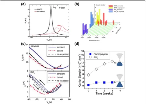
Figure 5(See legend on next page.)
Passivation of the SiO
2surface with a hydrophobic
buffer layer has been suggested as an effective route to
improve the interface properties of SiO
2. Two types of
buffer layers have been studied for this purpose:
self-assembled monolayers (SAMs) [72-77] and thin polymer
layers [78,79]. Lafkioti et al. reported that the intrinsic
charge neutrality of graphene was recovered and the
hysteresis of graphene FETs was dramatically reduced by
modifying the graphene/SiO
2interface with
hexamethyl-disilazane (HMDS) (Figure 4a) [73]. Wang et al. also
ob-served similar phenomena with alkyl-terminated SAM.
In both cases, the mobility of graphene increased
several-fold, as compared to devices on bare SiO
2. Representative
results for alkyl-SAM are shown in Figure 4b [77]. The
hydrophobic treatments eliminate SiOH groups and the
adsorbed water molecules at the graphene/SiO
2interface,
resulting in suppression of p-doping in graphene. In
addition, the scattering induced by charged impurities
and surface polar phonons can be screened due to the
in-crease of the graphene-substrate distance via interface
modification with HMDS or organosilane SAMs. Lee at al.
demonstrated that charged impurities were more
effect-ively screened by SAM with longer alkyl chain lengths by
showing that octadecyl-SAM (C18) resulted in smaller
Dirac voltage and higher mobility of graphene than
octyl-SAM (C8) [72].
According to a report by Sabri et al., deposition of a thin
polymeric layer (a 168 nm film of Parylene-C) on SiO
2provided the same effect as SAM treatment in terms of
re-duced hysteresis and enhanced mobility (Figure 4c) [78].
Recently, Shin et al. found that electrical reliability of
gra-phene FETs in an air ambient can be achieved by
introdu-cing an ultrathin fluoropolymer to the graphene/SiO
2interface [79]. With a 7-nm-thick CYTOP fluoropolymer,
the carrier density of graphene was changed negligibly
even after exposure of the device to an air ambient (RH ~
45%) for 3 weeks (Figure 4d). A highly hydrophobic buffer
such as the fluorinated buffer also contributes to recovery
of intrinsic charge neutrality, suppresses hysteresis, and
enhances mobility, as mentioned above. It is worth noting
that the unique wetting transparency of graphene [80]
pre-vents water molecules from being adsorbed on the
gra-phene surface integrated on the fluoropolymer, resulting
in excellent ambient stability of graphene FETs.
Modification of the graphene/target substrate interface
by SAM can be also used to tune the carrier type or
density, namely doping control, without compromising
the intrinsic electrical properties of graphene [81-84]:
SAMs terminated with various functional groups induce
n- or p-type doping of graphene by charge transfer from
a specific functional group or the built-in potential
gen-erated from the dipole moment of the SAM. Here, we
do not cover this in detail, but readers who are
inter-ested in this topic may refer to a recent in-depth review
[85]. In connection to this review it should be
men-tioned that the reported doping levels have shown a
wide range of variation in terms of the Dirac point even
when the same SAM (for example,
aminopropyltriethox-ysilane; APTES) was used [84,86-89]. This might be
at-tributable to the integrity of the SAM formed on SiO
2,
which sometimes depends sensitively on the chemistry
involved in SAM formation such as the treatment
methods (phase of SAM during the treatment) and
con-ditions (water content in the ambient atmosphere or
solvent) [90]. Hence, more studies are required to
ex-ploit SAM doping methods in practical applications
be-yond academic research based on SiO
2. For instance,
given that APTES SAM treatment can provide a more
effective and stable n-doping source [87,88] over other
doping methods, it is worthwhile to investigate how to
achieve a reliable doping level and whether this doping
method is also compatible with plastic substrates for
the application of APTES SAM to graphene flexible/
transparent electrodes. One of the sources of the
deg-radation of the doping strength is the desorption of
dopants in chemical doping methods when the doped
graphene sample is exposed to the air ambient [91]
while the formation of covalent bonding between the
SAM and the target substrate can guarantee
environ-mental doping stability.
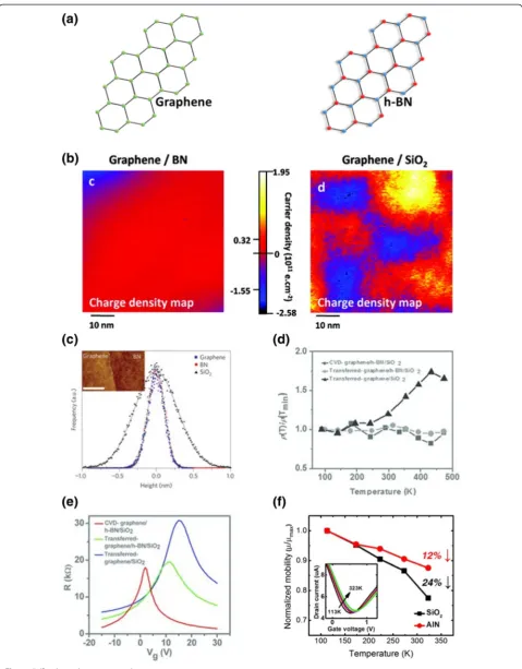
2.2.2 Substrates with high surface phonon energy
While the passivation of SiO
2with SAMs or functional
polymers is useful to considerably reduce the substrate
effects on the electrical characteristics of graphene FETs,
the carrier transport in graphene is still limited by
ther-mally excited surface phonons of SAMs or polymers,
es-pecially at room temperature. Hence, the combination of
(See figure on previous page.)graphene with substrates having high surface phonon
en-ergy is the most attractive way to achieve high
perform-ance graphene devices operated at room temperature.
One outstanding material for this purpose is hexagonal
boron nitride (h-BN) [92-98]. h-BN is an insulating
iso-morph of graphite (Figure 5a), a layered dielectric material
with a wide band gap of ~5.97 eV and a dielectric constant
of ~4 [92]. A planar, hexagonal lattice structure of the
h-BN layer is formed by strong ionic bonding between
boron and nitrogen atoms, which provides a chemically
inert, dangling-bond-free flat surface [96]. According to
Decker et al., these features of the h-BN surface induce
lower density of introduced charged impurities in
gra-phene and a considerable reduction of inhomogeneities
of charge density in graphene/h-BN, as compared to a
SiO
2substrate (Figure 5b) [97]. Ripples of graphene are
also suppressed on h-BN due to its atomically flat
sur-face (Figure 5c) and, even more importantly, the sursur-face
phonon energy of h-BN is two times larger than that of
SiO
2[92]. Significant enhancement of the electrical
char-acteristics of graphene devices can hence be expected by
the improved interface of the graphene/h-BN system. The
highest mobility value reported for CVD-graphene/h-BN
is 65 500 cm
2/Vs, which is ~ 30 times higher than that for
CVD-graphene/SiO
2[93].
Wang et al. investigated the effects of
graphene/sub-strate interfaces on the electrical performance of
gra-phene FETs with three different gragra-phene systems:
CVD-graphene transferred on SiO
2, CVD-graphene transferred
on h-BN flakes, and graphene directly grown on a
CVD-h-BN film [98]. The temperature dependence of
the graphene resistivity was negligible for
graphene/h-BN, indicating that no surface phonons were activated
up to room temperature in h-BN due to its high surface
phonon energy (Figure 5d). The graphene/h-BN interface
thus exhibited superior mobility, a narrower minimum
conductivity plateau, and a Dirac point close to zero, as
compared to the graphene/SiO
2interface (Figure 5e).
Su-perb performance of a graphene device was obtained when
a graphene/h-BN interface was created by sequential CVD
growth of graphene directly on CVD-grown h-BN on Cu
due to the absence of residues and adsorbates generated
from the transfer process.
While h-BN is an ideal substrate for high performance
graphene devices, it is still challenging to synthesize high
quality, large area h-BN films. Therefore, from a
prac-tical point of view for graphene electronics, it is
neces-sary to develop alternative, cost-effective substrates with
high surface phonon energy and with which it is easy to
obtain a large sized film with good reproducibility and
uniformity. A recent report from Oh et al. demonstrated
that aluminum nitride (AlN) substrate can serve as an
excellent alternative to h-BN with several of the
advan-tages mentioned above [99]. An ultrathin AlN film with
a smooth surface (Rq ~ 0.5 nm) was simply obtained over
a large area (4 inch wafer) by a plasma enhanced atomic
layer deposition (PE-ALD) method. Top gated graphene
FETs on an AlN substrate showed higher mobility than
devices on SiO
2, indicating the suppression of surface
pho-non scattering. The high surface phopho-non energy of AlN
(Table 2) resulted in weaker temperature dependence of
mobility (Figure 5f ). The RF cut-off frequency was thereby
significantly improved in graphene FETs on AlN (115
GHz), compared to those on SiO
2(55 GHz). Similar
en-hancement of the cut-off frequency (155 GHz) was also
reported by Wu et al. for a graphene FET on diamond-like
carbon (DLC) [100], which shows high surface phonon
energy (Table 2).
2.3 Interface engineering of graphene/gate dielectric
Integration of graphene with passive components such
as gate dielectrics is another important step to achieve
high performance graphene devices. Oxide materials
with a high dielectric constant (k) have been used as gate
dielectrics to fabricate top-gated graphene FETs because
high-k dielectrics enable low voltage operation of devices
by their high capacitance and also provide scaling
cap-ability [101-104]. In conventional electronics, high-k
di-electrics have been deposited by atomic layer deposition
(ALD), because this technique can produce ultrathin,
conformal oxide dielectrics with precisely controlled
thickness [105-109]. However, the basal plane of
gra-phene has few dangling bonds [110-113], which are
ne-cessary to induce the surface reaction of precursors in
the ALD process [114-116]. This unique feature of
the graphene surface results in irregular and poor film
formation of ALD-dielectrics on pristine graphene
[111,113,117]. ALD-dielectrics with a rough surface and
many pin-holes cause high leakage current, low
break-down voltage, and extrinsic scattering of charge carriers
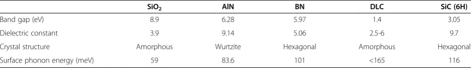
Table 2 Material properties of various substrates used in graphene devices
SiO2 AlN BN DLC SiC (6H)
Band gap (eV) 8.9 6.28 5.97 1.4 3.05
Dielectric constant 3.9 9.14 5.06 2.5-6 9.7
Crystal structure Amorphous Wurtzite Hexagonal Amorphous Hexagonal
Surface phonon energy (meV) 59 83.6 101 <165 116
Reproduced with permission [99]. Copyright 2014, AIP Publishing LLC.
at the graphene/high-k dielectric interface in graphene
FETs. To obtain high quality, uniform high-k
dielec-trics on graphene, the introduction of seeds on the
graphene surface has been proposed as an effective
means of fabricating graphene devices using the
ALD technique.
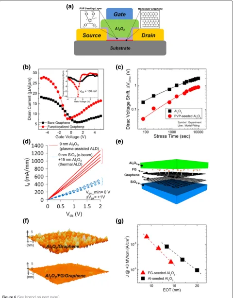
2.3.1 Introduction of seeding materials on graphene
Various materials have been used as seeding materials
for the formation of uniform, high quality high-k
di-electrics on graphene by ALD [113,118-126]. Kim et al.
proposed the use of a thin aluminum layer (thickness
1~2 nm) to deposit uniform Al
2O
3films on graphene
[119]. A native aluminum oxide is formed when the
thin Al layer is exposed to air, and this oxide provides
nucleation sites for the surface reactions during ALD
of Al
2O
3. Organic molecules or polymers have been
exploited as seeding layers for the integration of
dielec-trics and graphene [113,122-125]. One example is the
use of a poly(vinyl phenol) (PVP) film [125]. Shin et al.
prepared an ultrathin, cross-linked PVP seeding layer
(thickness ~5 nm) on a graphene surface by a spin-coating
method (Figure 6a). Due to abundant functional groups
in PVP such as hydroxyl and hydrocarbon, the Al
2O
3film deposited on the PVP seeding layer by ALD
was smooth (R
rms~0.5 nm) without pin-holes. The
electrical performance of top-gated graphene FETs
was considerably improved with PVP-seeded Al
2O
3,
compared to devices with Al
2O
3deposited on bare
graphene. Specifically, the drain current and
transcon-ductance were enhanced, resulting in a more than
five-fold increase of mobility (Figure 6b). In particular,
a graphene FET with PVP-seeded Al
2O
3showed a
sup-pressed Dirac point shift under a gate bias stress
condition (Figure 6c). A recent study by Kim et al.
sug-gested that quantum dot (CdSe) arrays formed on
gra-phene also can serve as a seeding layer for the effective
ALD of high-k hafnium oxide on graphene [126].
2.3.2 Functionalization of graphene
To generate seeding sites on graphene, functional groups
can be directly introduced to the graphene surface by
oxidizing carbon atoms of graphene [112,127-129]. Lee
et al. reported on graphene functionalization using
ozone (O
3) during ALD of Al
2O
3[112,127]. An ultrathin
(~1 nm), smooth (R
rms~0.1 nm) seed layer was formed
on graphene by O
3treatment in the presence of a
tri-methylaluminum precursor. Gentle O
3treatment
condi-tions (at 25°C for 20s) induced negligible defects on
graphene while its surface was partially functionalized
with epoxide groups. A 15-nm-thick Al
2O
3layer was
uniformly formed by O
3based ALD, resulting in high
performance, top-gated graphene FETs with carrier
mo-bility of 5 000 cm
2/Vs, low V
dirachysteresis, and low
leakage current. In the same context, Nayfeh et al.
dem-onstrated that a remote O
2plasma-assisted ALD
tech-nique produced a 9-nm-thick Al
2O
3layer with better
conformal coverage and lower roughness, compared to
Al
2O
3films deposited by thermal ALD [128]. They
re-ported an increase of the defect level in graphene on the
basis of Raman measurements, indicating that graphene
was functionalized during the O
2plasma-assisted ALD
process. Both drain current and mobility were enhanced
in graphene FETs with 9-nm-thick Al
2O
3by
plasma-assisted ALD, compared to those obtained with a
9-nm-thick, e-beam-evaporated SiO
2interfacial layer plus a
15-nm-thick Al
2O
3layer by thermal ALD (Figure 6d).
In order to avoid uncontrolled damage of graphene in
O
2plasma or O
3-assisted ALD, Shin et al. proposed a
novel approach for reliable high-k dielectric formation
on graphene with ALD by introducing an additional
functionalized graphene single layer as an ultrathin seed
layer on the graphene channel (Figure 6e) [129]. Pristine
graphene was transferred to a target substrate and then
functionalized (O
2plasma treated) graphene was stacked
on the pristine graphene prior to conducting the ALD
process. Al
2O
3was deposited via conventional thermal
ALD on a functionalized graphene layer where the surface
(See figure on previous page.)Figure 6Seeding ALD of high-k dielectric on graphene. a, Schematic diagram showing top-gate graphene FET structure with PVP-seeded Al2O3 gate dielectric. Reproduced with permission [125]. Copyright 2012, AIP Publishing LLC.b, Transfer characteristics (Id-Vg) of top-gate graphene FET before (black square) and after (red circle) the graphene channel is deposited with PVP. Inset: transconductance of the graphene FETs with different gate dielectrics as a function of gate voltage. Reproduced with permission [125]. Copyright 2012, AIP Publishing LLC.c, The time-dependent VDiracshift of graphene FET before (black square) and after (red circle) the graphene channel is deposited with PVP. Reproduced with permission [125]. Copyright 2012, AIP Publishing LLC.d, Output characteristics (Id-Vd) of transistors based on CVD monolayer graphene with 9nm Al2O3(red line) and 24 nm heterogeneous integrated dielectrics (dashed blue line) via different depositing methods. Reproduced with permission [128]. Copyright 2011, IEEE. e, Schematic diagram presenting the functionalized graphene-seeded Al2O3stack on graphene. Reproduced with permission [129]. Copyright 2013, American Chemical Society.f, Surface morphology of the Al2O3films deposited on graphene (top) and functionalized graphene (bottom). Scan size: 1 × 1μm2. Reproduced with permission [129]. Copyright 2013, American Chemical Society.g, Leakage current densities (at +3 MV/cm2) versus EOT for dielectrics with functionalized graphene seed layer (red triangle) and Al seed layer (black square) on graphene. Reproduced with permission [129]. Copyright 2013, American Chemical Society.
has abundant, oxidized carbon moieties. Al
2O
3deposited
on the functionalized graphene/pristine graphene stack
exhibited excellent uniformity with low defect density
(Figure 6f; R
rms~0.3 nm). In addition, capacitors with
functionalized graphene seeded Al
2O
3showed lower
leak-age current density for the same effective oxide thickness
(EOT), compared to those with Al-seeded Al
2O
3: this is a
considerable advantage of this approach in terms of
fur-ther scaling of gate oxide thickness (Figure 6g).
3 Conclusions
This review highlighted the importance of interface
en-gineering for high performance graphene devices by
considering each interface encountered during the
fabri-cation of graphene devices, from the graphene/metal
growth substrate to graphene/high-k gate dielectrics. For
effective delamination and transfer of graphene,
adhe-sion at the interface of the graphene/metal growth
sub-strate or graphene/target subsub-strate should be engineered
by appropriate weakening or strengthening methods for
those interfaces. In terms of graphene delamination using
polymer adhesives or a carrier layer, questions remains
about which functional groups in the polymer play a
crit-ical role to induce delamination of graphene. This should
be investigated systematically by applying polymers having
various functional groups to graphene delamination
sys-tems, in conjunction with an investigation of doping
effects that might be induced from the functional groups
of polymers.
After graphene is transferred onto a target substrate,
interfacial issues arise from the atom-thickness of
gra-phene and the surface-gragra-phene interactions. Since the
surface states of substrates significantly affect the overall
electrical properties of graphene devices, substrates with
a chemically inert, dangling-bond-free flat surface as well
as high surface phonon energy are highly demanded.
Al-though h-BN is an ideal substrate in terms of realizing
high performance graphene electronics, obtaining
reli-able, large-area synthesis methods for h-BN beyond
mechanical exfoliation is still a challenging issue. On the
other hand, alternative substrate materials, such as AlN,
are attractive, as highlighted in this review.
To deposit a high-k dielectric using ALD, it is
neces-sary to introduce seed materials onto graphene due to
the chemically inert surface of graphene or to generate
seeding centers on graphene itself. These approaches
cause heterogeneous dielectric stacks (or interfaces) and
give rise to difficulty in controlling the film thickness,
thereby constraining the scaling of gate dielectric
thick-ness. A novel approach for the deposition of gate
dielec-trics therefore should be explored to achieve a single
component gate dielectric that forms a homogeneous
interface without the application of additive seed layers.
One example would be the deposition of ultrathin (less
than 10 nm) polymer dielectrics by the initiated CVD
method, which is under investigation by our group. The
use of ultrathin polymer dielectrics in graphene FETs
would also be desirable for the development of flexible
electronic devices.
Intensive studies in recent decades have provided a
great deal of insight into the important role of interface
engineering in graphene systems, and have opened up
opportunities for the realization of high performance
graphene devices. We expect that knowledge
accumu-lated from graphene will be extended to emerging 2D
materials for the enhancement and optimization of
device performance.
Competing interests
The authors declare that they have no competing interests.
Authors’contributions
DYJ and SYY equally contributed to this work in the manuscript preparation. All authors read and approved the final manuscript.
Acknowledgements
This work was supported by the IT R&D program (10044412), the Global Frontier Research Center for Advanced Soft Electronics (2011–0031640), the Basic Science Research Program (2010–0029132) and Nano-Material Technology Development Program (2012M3A7B4049807).
Received: 11 December 2014 Accepted: 5 January 2015
References
1. KS Novoselov, AK Geim, SV Morozov, D Jiang, Y Zhang, SV Dubonos, IV Grigorieva, AA Firsov, Electric field effect in atomically thin carbon films. Science306, 666–669 (2004)
2. KS Novoselov, AK Geim, SV Morozov, D Jiang, MI Katsnelson IV, SVD Grigorieva, AA Firsov, Two-dimensional gas of massless Dirac fermions in graphene. Nature438, 197–200 (2005)
3. KI Bolotin, KJ Sikes, Z Jiang, M Klima, G Fudenberg, J Hone, P Kim, HL Stormer, Ultrahigh electron mobility in suspended graphene. Solid. State. Commun.146, 351–355 (2008)
4. KS Novoselov, D Jiang, F Schedin, TJ Booth, VV Khotkevich, SV Morozov, AK Geim, Two-dimensional atomic crystals. Proc. Natl. Acad. Sci. U. S. A.102, 10451–10453 (2005)
5. SV Morozov, KS Novoselov, MI Katsnelson, F Schedin, DC Elias, JA Jaszczak, AK Geim, Giant intrinsic carrier mobilities in graphene and its bilayer. Phys. Rev. Lett.100, 016602 (2008)
6. Y Zhang, JW Tan, HL Stormer, P Kim, Experimental observation of the quantum hall effect and Berry’s phase in graphene. Nature438, 201–204 (2005) 7. RR Nair, P Blake, AN Grigorenko, KS Novoselov, TJ Booth, T Stauber, NMR
Peres, AK Geim, Fine structure constant defines visual transparency of graphene. Science320, 1308 (2008)
8. C Lee, X Wei, JW Kysar, J Hone, Measurement of the elastic properties and intrinsic strength of monolayer graphene. Science321, 385–388 (2008) 9. AK Geim, KS Novoselov, The rise of graphene. Nat. Mater.6, 183–191 (2007) 10. AK Geim, Graphene: status and prospects. Science324, 1530–1534 (2009) 11. SK Hong, KY Kim, TY Kim, JH Kim, SW Park, JH Kim, BJ Cho, Electromagnetic
interference shielding effectiveness of monolayer graphene. Nanotechnol. 23, 455704 (2012)
12. JT Kim, J Kim, H Choi, CG Choi, S-Y Choi, Graphene-based photonic devices for soft hybrid optoelectronic systems. Nanotechnol.23, 344005 (2012) 13. SH Lee, M Choi, TT Kim, S Lee, M Liu, X Yin, HK Choi, SS Lee, CG Choi, S-Y
Choi, X Zhang, B Min, Switching terahertz waves with gate-controlled active graphene metamaterials. Nat. Mater.11, 936–941 (2012)
15. JH Kim, J Seo, DG Kwon, JA Hong, J Hwang, HK Choi, J Moon, JI Lee, DY Jung, S-Y Choi, Y Park, Carrier injection efficiencies and energy level alignments of multilayer graphene anodes for organic light-emitting diodes with different hole injection layers. Carbon79, 623–630 (2014)
16. X Li, W Cai, J An, S Kim, J Nah, D Yang, R Piner, A Velamakanni, I Jung, E Tutuc, SK Banerjee, L Colombo, RS Ruoff, Large-area synthesis of high-quality and uniform graphene films on copper foils. Science324, 1312–1314 (2009) 17. X Li, CW Magnuson, A Venugopal, J An, JW Suk, B Han, M Boryslak, W Cai,
A Velamakanni, Y Zhu, L Fu, EM Vogel, E Voelkl, L Colombo, RS Ruoff, Graphene films with large domain size by a two-step chemical vapor deposition process. Nano Lett.10, 4328–4334 (2010)
18. H Wang, G Wang, P Bao, S Yang, W Zhu, X Xie, WJ Zhang, Controllable synthesis of submillimeter single-crystal monolayer graphene domains on copper foils by suppressing nucleation. J. Am. Chem. Soc.134, 3627–3630 (2012) 19. S Bae, H Kim, Y Lee, X Xu, JS Park, Y Zheng, J Balakrishnan, T Lei, HR Kim, YI
Song, YJ Kim, KS Kim, B Ozyilmaz, JH Ahn, BH Hong, S Iijima, Roll-to-roll production of 30-inch graphene films for transparent electrodes. Nat. Nanotechnol.5, 574–578 (2010)
20. S Chen, H Ji, H Chou, Q Li, H Li, JW Suk, R Piner, L Liao, W Cai, RS Ruoff, Millimeter-size single-crystal graphene by suppressing evaporative loss of Cu during low pressure chemical vapor deposition. Adv. Mater. 25, 2062–2065 (2013)
21. J Lee, J Baek, GH Ryu, MJ Lee, S Oh, SK Hong, BH Kim, SH Lee, BJ Cho, Z Lee, S Jeon, High-angle tilt boundary graphene domain recrystallized from mobile hot-wire-assisted chemical vapor deposition system. Nano Lett. 14, 4352–4359 (2014)
22. JH Mun, BJ Cho, Synthesis of monolayer graphene having a negligible amount of wrinkles by stress relaxation. Nano Lett.13, 2496–2499 (2013) 23. L Brown, EB Lochocki, J Avila, CJ Kim, Y Ogawa, RW Havener, DK Kim, EJ Monkman, DE Shai, HI Wei, MP Levendorf, M Asensio, KM Shen, J Park, Polycrystalline graphene with single crystalline electronic structure. Nano Lett.14, 5706–5711 (2014)
24. J Chen, Y Wen, Y Guo, B Wu, L Huang, Y Xue, D Geng, D Wang, G Yu, Y Liu, Oxygen-aided synthesis of polycrystalline graphene on silicon dioxide substrates. J. Am. Chem. Soc.133, 17548–17551 (2011)
25. JH Lee, EK Lee, WJ Joo, Y Jang, BS Kim, JY Lim, SH Choi, SJ Ahn, JR Ahn, MH Park, CW Yang, BL Choi, SW Hwang, D Whang, Wafer-scale growth of single-crystal monolayer graphene on reusable hydrogen-terminated germanium. Science344, 286–289 (2014)
26. Q Yu, LA Jauregui, W Wu, R Colby, J Tian, Z Su, H Cao, Z Liu, D Pandey, D Wei, TF Chung, P Peng, NP Guisinger, EA Stach, J Bao, SS Pei, YP Chen, Control and characterization of individual grains and grain boundaries in graphene grown by chemical vapor deposition. Nat. Mater.10, 443–449 (2011)
27. Y Zhang, L Zhang, P Kim, M Ge, Z Li, C Zhou, Vapor trapping growth of single-crystalline graphene flowers: synthesis, morphology, and electronic properties. Nano Lett.12, 2810–2816 (2012)
28. H Zhou, WJ Yu, L Liu, R Cheng, Y Chen, X Huang, Y Liu, Y Wang, Y Huang, X Duan, Chemical vapor deposition growth of large single crystals of monolayer and bilayer graphene. Nat. Commun.4, 2096 (2013) 29. AW Tsen, L Brown, MP Levendorf, F Ghahari, PY Huang, RW Havener, CS
Ruiz-Vargas, DA Muller, P Kim, J Park, Tailoring electrical transport across grain boundaries in polycrystalline graphene. Science336, 1143–1146 (2012) 30. CW Chen, F Ren, GC Chi, SC Hung, YP Huang, Effects of semiconductor
processing chemicals on conductivity of graphene. J. Vac. Sci. Technol. B30, 040602 (2012)
31. J Chan, A Venugopal, A Pirkle, S McDonnell, D Hinojos, CW Magnuson, RS Ruoff, L Colombo, RM Wallace, EM Vogel, Reducing extrinsic performance-limiting factors in graphene grown by chemical vapor deposition. ACS Nano 6, 3224–3229 (2012)
32. A Pirkle, J Chan, A Venugopal, D Hinojos, CW Magnuson, S McDonnell, L Colombo, EM Vogel, RS Ruoff, RM Wallace, The effect of chemical residues on the physical and electrical properties of chemical vapor deposited graphene transferred to SiO2. Appl. Phys. Lett.99, 122108 (2011) 33. Z Cheng, Q Zhou, C Wang, Q Li, C Wang, Y Fang, Toward intrinsic graphene
surfaces: a systematic study on thermal annealing and wet-chemical treatment of SiO2-supported graphene devices. Nano Lett.11, 761–771 (2011) 34. C Casiraghi, S Pisana, KS Novoselov, AK Geim, AC Ferrari, Raman fingerprint of
charged impurities in graphene. Appl. Phys. Lett.91, 233108 (2007)
35. S Ryu, L Liu, S Berclaud, YJ Yu, H Liu, P Kim, GW Flynn, LE Brus, Atmospheric oxygen binding hole doping in deformed graphene on a SiO2substrate. Nano Lett.10, 4944–4951 (2010)
36. X Li, Y Zhu, W Cai, M Borysiak, B Han, D Chen, RD Piner, L Colombo, RS Ruoff, Transfer of large-area graphene films for high-performance transparent conductive electrodes. Nano Lett.9, 4359–4363 (2009) 37. J Song, F-Y Kam, R-Q Png, W-L Seah, J-M Zhou, G-K Lim, PKH Ho, L-L Chua,
A general method for transferring graphene onto soft surfaces. Nat. Nanotechnol.8, 356–362 (2013)
38. J Kang, S Hwang, JH Kim, MH Kim, J Ryu, SJ Seo, BH Hong, MK Kim, J-B Choi, Efficient transfer of large-area graphene films onto rigid substrates by hot pressing. ACS Nano6, 5360–5365 (2012)
39. JW Suk, A Kitt, CW Magnuson, Y Hao, S Ahmed, J An, AK Swan, BB Goldberg, RS Ruoff, Transfer of CVD-grown monolayer graphene onto arbitrary substrates. ACS Nano5, 6916–6924 (2011)
40. X-D Chen, Z-B Liu, C-Y Zheng, F Xing, X-Q Yan, Y Chen, J-G Tian, High quality and efficient transfer of large-area graphene films onto different substrates. Carbon56, 271–278 (2013)
41. X Liang, BA Sperling, I Calizo, G Cheng, CA Hacker, Q Zhang, Y Obeng, K Yan, H Peng, Q Li, X Zhu, H Yuan, AR Hight Walker, Z Liu, L-M Peng, CA Richter, Toward clean and crackles transfer of graphene. ACS Nano 5, 9144–9153 (2011)
42. HK Choi, JY Kim, HY Jeong, CG Choi, S-Y Choi, Characterization of chemical vapor deposition-grown graphene films with various etchants. Carbon Lett. 13, 44–47 (2012)
43. JW Suk, WH Lee, J Lee, H Chou, RD Piner, Y Hao, D Akinwande, RS Ruoff, Enhancement of the electrical properties of graphene grown by chemical vapor deposition via controlling the effects for polymer residue. Nano Lett. 13, 1462–1467 (2013)
44. Y Wang, Y Zheng, X Xu, E Dubuisson, Q Bao, J Lu, KP Loh, Electrochemical delamination of CVD-grown graphene film: Toward the recyclable use of copper catalyst. ACS Nano5, 9927–9933 (2011)
45. CJL de la Rosa, J Sun, N Lindvall, MT Cole, Y Nam, M Loffler, E Olsson, KBK Teo, A Yurgens, Frame assisted H2O electrolysis induced H2bubbling transfer of large area graphene grown by chemical vapor deposition on Cu. Appl. Phys. Lett.102, 022101 (2013)
46. L Gao, W Ren, H Xu, L Jin, Z Wang, T Ma, L-P Ma, Z Zhang, Q Fu, L-M Peng, X Bao, H-M Cheng, Repeated growth and bubbling transfer of graphene with millimeter-size single-crystal grains using platinum.
Nat. Commun.3, 699 (2012)
47. X Wang, L Tao, Y Hao, Z Liu, H Chou, I Kholmanov, S Chen, C Tan, N Jayant, Q Yu, D Akinwande, RS Ruoff, Direct delamination of graphene for high-performance plastic electronics. Small10, 694–698 (2014)
48. CT Cherian, F Giustiniano, I Martin-Fernandez, H Andersen, J Balakrishnan, B Ozyilmaz, Bubble-free electrochemical delamination of CVD graphene films, Small. (2014).doi:10.1002/smll.201402024 .
49. T Ciuk, I Pasternak, A Krajewska, J Sobieski, P Caban, J Szmidt, W Strupinski, Properties of chemical vapor deposition graphene transferred by high-speed electrochemical delamination. J. Phys. Chem. C117, 20833–20837 (2013) 50. PW Sutter, JI Flege, EA Sutter, Epitaxial graphene on ruthenium.
Nat. Mater.7, 406–411 (2008)
51. J Coraux, AT N’Diaye, M Engler, C Busse, D Wall, N Buckanie, FJMZ Heringdorf, R van Gastel, B Poelsema, T Michely, Growth of graphene on Ir(111). New J. Phys.11, 023006 (2009)
52. DY Jung,A Study on Graphene Synthesis by CVD Method and Graphene Transfer Method via Electrochemical Delamination. Master’s thesis (Korea Advanced Institute of Science and Technology, Daejeon, Republic of Korea, 2014), p. 53
53. T Yoon, WC Shin, TY Kim, JH Mun, T-S Kim, BJ Cho, Direct measurement of adhesion energy of monolayer graphene as-grown on copper and its application to renewable transfer process. Nano Lett.12, 1448–1452 (2012) 54. WC Shin, T Yoon, JH Mun, TY Kim, S-Y Choi, T-S Kim, BJ Cho, Doping
suppression and mobility enhancement of graphene transistors fabricated using an adhesion promoting dry transfer process. Appl. Phys. Lett. 103, 243504 (2013)
55. W Jung, D Kim, M Lee, S Kim, J-H Kim, C-S Han, Ultraconformal contact transfer of monolayer graphene on metal to various substrates. Adv. Mater. 26, 6394–6400 (2014)
56. SY Yang, JG Oh, DY Jung, H Choi, CH Yu, J Shin, C-G Choi, BJ Cho, S-Y Choi, Metal-etching-free direct delamination and transfer of single-layer graphene with a high degree of freedom, Small. (2014).doi:10.1002/smll.201401196 57. P Blake, EW Hill, AH Castro Neto, KS Novoselov, D Jiang, R Yang, TJ Booth,
AK Geim, Making graphene visible. Appl. Phys. Lett. 91, 063124 (2007)
58. DSL Abergel, A Russell, VI Fal’ko, Visibility of graphene flakes on a dielectric substrate. Appl. Phys. Lett.91, 063125 (2007)
59. QH Wang, Z Jin, KK Kim, AJ Hilmer, GLC Paulus, C-J Shih, M-H Ham, JD Sanchez-Yamagishi, K Watanabe, T Taniguchi, J Kong, P Jarillo-Herrero, MS Strano, Understanding and controlling the substrate effect on graphene electron-transfer chemistry via reactivity imprint lithography.
Nat. Chem.4, 724–732 (2012)
60. J-H Chen, C Jang, S Xiao, M Ishigami, MS Fuhrer, Intrinsic and extrinsic performance limits of graphene devices on SiO2. Nat. Nanotechnol. 3, 206–209 (2008)
61. KI Bolotin, KJ Sikes, J Hone, HL Stormer, P Kim, Temperature-dependent transport in suspended graphene. Phys. Rev. Lett.101, 096802 (2008) 62. JP Robinson, H Schomerus, L Oroszlany, VI Fal’ko, Adsorbate-limited
conductivity of graphene. Phys. Rev. Lett.101, 196803 (2008) 63. DB Farmer, R Golizadeh-Mojarad, V Perebeinos, Y-M Lin, GS Tulevski, JC
Tsang, P Avouris, Chemical doping and electron–hole conduction asymmetry in graphene devices. Nano Lett.9, 392–399 (2009) 64. J-H Chen, C Jang, S Adam, MS Fuhrer, ED Williams, M Ishigami,
Charged-impurity scattering in graphene. Nat. Phys.4, 377–381 (2008) 65. J-H Chen, C Jang, M Ishigami, S Xiao, WG Cullen, ED Williams, MS Fuhrer,
Diffusive charge transport in graphene on SiO2. Solid. State. Commun. 149, 1080–1086 (2009)
66. T Lohmann, K von Klitzing, JH Smet, Four-terminal magneto-transport in graphene p-n junctions created by spatially selective doping. Nano Lett. 9, 1973–1979 (2009)
67. O Leenaerts, B Partoens, FM Peeters, Adsorption of H2O, NH3, CO, NO2, and NO on graphene: A first-principles study. Phys. Rev. B.77, 125416 (2008) 68. TO Wehling, MI Katsnelson, AI Lichtenstein, Adsorbates on graphene:
Impurity states and electron scattering. Chem. Phys. Lett. 476, 125–134 (2009)
69. D-W Shin, HM Lee, SM Yu, K-S Lim, JH Jung, M-K Kim, S-W Kim, J-H Han, RS Ruoff, J-B Yoo, A facile route to recover intrinsic graphene over large scale. ACS Nano6, 7781–7788 (2012)
70. P Joshi, HE Romero, AT Neal, VK Toutam, SA Tadigadapa, Instrinsic doping and gate hysteresis in graphene field effect devices fabricated on SiO2 substrates. J. Phys. Condens. Matter22, 334214 (2010)
71. H Wang, Y Wu, C Cong, J Shang, T Yu, Hysteresis of electronic transport in graphene transistors. ACS Nano4, 7221–7228 (2010)
72. WH Lee, J Park, Y Kim, KS Kim, BH Hong, K Cho, Control of graphene field-effect transistors by interfacial hydrophobic self-assembled monolayers. Adv. Mater.23, 3460–3464 (2011)
73. M Lafkioti, B Krauss, T Lohmann, U Zschieschang, H Klauk, K Klitzing, JH Smet, Graphene on a hydrophobic substrate: doping reduction and hysteresis suppression under ambient conditions. Nano Lett.10, 1149–1153 (2010) 74. SF Chowdhury, S Sonde, S Rahimi, L Tao, S Banerjee, D Akinwande,
Improvement of graphene field-effect transistors by hexamethyldisilazane surface treatment. Appl. Phys. Lett.105, 033117 (2014)
75. Z Liu, AA Bol, W Haensch, Large-scale graphene transistors with enhanced performance and reliability based on interface engineering by phenylsilane self-assembled monolayers. Nano Lett.11, 523–528 (2011)
76. H Lv, H Wu, K Xiao, W Zhu, H Xu, Z Zhang, H Qian, Graphene mobility enhancement by organosilane interface engineering. Appl. Phys. Lett. 102, 183107 (2013)
77. X Wang, J-B Xu, C Wang, J Du, W Xie, High performance graphene devices on SiO2/Si substrate modified by highly ordered self-assembled monolayers. Adv. Mater.23, 2464–2468 (2011)
78. SS Sabri, PL Levesque, CM Aguirre, J Guillemette, R Martel, T Szkopek, Graphene field effect transistors with parylene gate dielectric. Appl. Phys. Lett.95, 242104 (2009)
79. WC Shin, S Seo, BJ Cho, Highly air-stable electrical performance of graphene field effect transistors by interface engineering with amorphous fluoropolymer. Appl. Phys. Lett.98, 153505 (2011)
80. J Rafiee, X Mi, H Gullapalli, AV Thomas, F Yavari, Y Shi, PM Ajayan, NA Koratkar, Wetting transparency of graphene. Nat. Mater.
11, 217–222 (2012)
81. N Cernetic, S Wu, JA Davies, BW Krueger, DO Hutchins, X Xu, H Ma, AK-Y Jen, Systematic doping control of CVD graphene transistors with functionalized aromatic self-assembled monolayers. Adv. Funct. Mater.24, 3464–3470 (2014) 82. K Yokota, K Takai, T Enoki, Carrier control of graphene driven by the
proximity effect of functionalized self-assembled monolayers. Nano Lett. 11, 3669–3675 (2011)
83. R Wang, S Wang, D Zhang, Z Li, Y Fang, X Qiu, Control of carrier type and density in exfoliated graphene by interface engineering. ACS Nano 5, 408–412 (2011)
84. Z Yan, Z Sun, W Lu, J Yao, Y Zhu, JM Tour, Controlled modulation of electronic properties of graphene by self-assembled monolayers on SiO2 substrates. ACS Nano5, 1535–1540 (2011)
85. H Chen, X Guo, Unique role of self-assembled monolayers in carbon nanomaterials-based field-effect transistors. Small9, 1144–1159 (2013) 86. S Wang, S Suzuki, K Furukawa, CM Orofeo, M Takamura, H Hibino, Selective
charge doping of chemical vapor deposition-grown graphene by interface modification. Appl. Phys. Lett.103, 253116 (2013)
87. Y Kim, J Park, J Kang, JM Yoo, K Choi, ES Kim, J-B Choi, C Hwang, KS Novoselov, BH Hong, A highly conducting graphene film with dual-side molecular n-doping. Nanoscale6, 9545–9549 (2014)
88. J Park, WH Lee, S Huh, SH Sim, SB Kim, K Cho, BH Hong, KS Kim, Work-function engineering of graphene electrodes by self-assembled monolayers for high-performance organic field-effect transistors. J. Phys. Chem. Lett.2, 841–845 (2011)
89. R Shi, H Xu, B Chen, Z Zhang, L-M Peng, Scalable fabrication of graphene devices through photolithography. Appl. Phys. Lett.102, 113102 (2013) 90. J Kim, P Seidler, LS Wan, C Fill, Formation, structure, and reactivity of
amino-terminated organic films on silicon substrates. J. Colloid Interface Sci. 329, 114–119 (2009)
91. JH Bong, O Sul, A Yoon, S-Y Choi, BJ Cho, Facile graphene n-doping by wet chemical treatment for electronic applications. Nanoscale6, 8503–8508 (2014) 92. CR Dean, AF Young, I Meric, C Lee, L Wang, S Sorgenfrei, K Watanabe,
T Taniguchi, P Kim, KL Shepard, J Hone, Boron nitride substrates for high-quality graphene electronics. Nat. Nanotechnol.5, 722–726 (2010) 93. N Petrone, CR Dean, I Meric, AM van der Zande, PY Huang, L Wang, D
Muller, KL Shepard, J Hone, Chemical vapor deposition-derived graphene with electrical performance of exfoliated graphene. Nano Lett.12, 2751–2756 (2012) 94. E Kim, N Jain, Y Xu, B Yu, Logic Inverter Implemented with CVD-assembled
graphene FET on hexagonal boron nitride. IEEE Trans. Nanotechnol. 11, 619–623 (2012)
95. MS Bresnehan, MJ Hollander, M Wetherington, M LaBella, KA Trumbull, R Cavalero, DW Snyder, JA Robinson, Integration of hexagonal boron nitride with quasi-freestanding epitaxial graphene: Toward wafer-scale, high performance devices. ACS Nano6, 5234–5241 (2012)
96. C Dean, AF Young, L Wang, I Meric, G-H Lee, K Watanabe, T Taniguchi, K Shepard, P Kim, J Hone, Graphene based heterostructures. Solid. State. Commun.152, 1275–1282 (2012)
97. R Decker, Y Wang, VW Brar, W Regan, H-Z Tsai, Q Wu, W Gannett, A Zettl, MF Crommie, Local electronic properties of graphene on a BN substrate via scanning tunneling microscopy. Nano Lett.11, 2291–2295 (2011)
98. M Wang, SK Jang, W-J Jang, M Kim, S-Y Park, S-W Kim, S-J Kahng, J-Y Choi, RS Ruoff, YJ Song, S Lee, A platform for large-scale graphene electronics– CVD growth of single-layer graphene on CVD-grown hexagonal boron nitride. Adv. Mater.25, 2746–2752 (2013)
99. JG Oh, SK Hong, C-K Kim, JH Bong, J Shin, S-Y Choi, BJ Cho, High performance graphene field-effect transistors on an aluminum nitride substrate with high surface phonon energy. Appl. Phys. Lett.104, 193112 (2014)
100. Y Wu, Y Lin, AA Bol, KA Jenkins, F Xia, DB Farmer, Y Zhu, P Avouris, High-frequency, scaled graphene transistors on diamond-like carbon. Nature472, 74–78 (2011)
101. F Schwierz, Graphene transistors Nat Nanotechnol5, 487–496 (2010) 102. L Liao, J Bai, R Cheng, YC Lin, S Jiang, Y Huang, X Duan, Top-gated
graphene nanoribbon transistors with ultrathin high-k dielectrics. Nano Lett. 10, 1917–1921 (2010)
103. A Javey, H Kim, M Brink, Q Wang, A Ural, J Guo, P Mcintyre, P Mceuen, M Lundstrom, H Dai, High-k dielectrics for advanced carbon-nanotube transistors and logic gates. Nat. Mater.1, 241–246 (2002) 104. J Robertson, High dielectric constant oxides Eur. Phys. J. Appl. Phys.
28, 265–291 (2004)
105. M Leskela, M Ritala, Atomic layer deposition (ALD): from precursors to thin film structures. Thin Solid Films409, 138–146 (2002)
106. M Ritala, K Kukli, A Rahtu, PI Raisanen, M Leskela, T Sajavaara, J Keinonen, Atomic layer deposition of oxide thin films with metal alkoxides as oxygen sources. Science288, 319–321 (2000)
108. M Ritala, M Leskela, JP Dekker, C Mutsaers, PJ Soininen, J Skarp, Perfectly conformal TiN and Al2O3films deposited by atomic layer deposition. Chem. Vap. Deposition.5, 7–9 (1999)
109. K Kukli, J Ihanus, M Ritala, M Leskela, Tailoring the dielectric properties of HfO2-Ta2O5nanolaminates. Appl. Phys. Lett.68, 3737–3739 (1996) 110. FH Yang, RT Yang, Ab initio molecular orbital study of adsorption of atomic
hydrogen on graphite: insight into hydrogen storage in carbon nanotubes. Carbon40, 437–444 (2002)
111. Y Xuan, YQ Wu, T Shen, M Qi, MA Capano, JA Cooper, PD Ye, Atomic-layer-deposited nanostructures for graphene-based nanoelectronics. Appl. Phys. Lett. 92, 013101 (2008)
112. B Lee, SY Park, HC Kim, KJ Cho, EM Vogel, MJ Kim, RM Wallace, J Kim, Conformal Al2O3dielectric layer deposited by atomic layer deposition for graphene based nanoelectronics. Appl. Phys. Lett.92, 203102 (2008) 113. X Wang, SM Tabakman, H Dai, Atomic layer deposition of metal oxides on
pristine and functionalized graphene. J. Am. Chem. Soc.130, 8152–8153 (2008) 114. SM George, AW Ott, JW Klaus, Surface chemistry for atomic layer growth. J.
Phys. Chem.100, 13121–13131 (1996)
115. RL Puurunen, Surface chemistry of atomic layer deposition: a case study for the trimethylaluminium/water process. J. Appl. Phys.97, 121301 (2005) 116. SM George, Atomic layer deposition: an overview. Chem. Rev.110, 111–131 (2010) 117. NY Garces, VD Wheeler, DK Gaskill, Graphene functionalization and seeding
for dielectric deposition and device integration. J. Vac. Sci. Technol. B30, 030801 (2012)
118. MJ Hollander, A Agrawal, MS Bresnehan, M LaBella, KA Trumbull, R Cavalero, DW Snyder, S Datta, JA Robinson, Heterogeneous integration of hexagonal boron nitride on bilayer quasi-free-standing epitaxial graphene and its impact on electrical transport properties. Phys. Stat. Solidi. A. 210, 1062–1070 (2013)
119. S Kim, J Nah, I Jo, D Shahrjerdi, L Colombo, Z Yao, E Tutuc, SK Banerjee, Realization of a high mobility dual-gated graphene field-effect transistor with Al2O3dielectric. Appl. Phys. Lett.94, 062107 (2009)
120. S McDonnell, A Azcatl, G Mordi, C Floresca, A Pirkle, L Colombo, J Kim, M Kim, RM Wallace, Scaling of HfO2dielectric on CVD graphene. Appl. Surf. Sci. 294, 95–99 (2014)
121. MJ Hollander, M LaBella, ZR Hughes, M Zhu, KA Trumbull, R Cavalero, DW Snyder, X Wang, E Hwang, S Datta, JA Robinson, Enhanced transport and transistor performance with oxide seeded high-k gate dielectrics on wafer-scale epitaxial graphene. Nano Lett.11, 3601–3607 (2011) 122. DB Farmer, HY Chiu, YM Lin, KA Jenkins, F Xia, P Avouris, Utilization of a
buffered dielectric to achieve high field-effect carrier mobility in graphene transistors. Nano Lett.9, 4474–4478 (2009)
123. JMP Alaboson, QH Wang, JD Emery, AL Lipson, MJ Bedzyk, JW Elam, MJ Pellin, MC Hersam, Seeding atomic layer deposition of high-k dielectrics on epitaxial graphene with organic self-assembled monolayers. ACS Nano5, 5223–5232 (2011) 124. VK Sangwan, D Jariwala, SA Filippone, HJ Karmel, JE Johns, JMP Alaboson,
TJ Marks, LJ Lauhon, MC Hersam, Quantitatively enhanced reliability and uniformity of high-k dielectrics on graphene enabled by
self-assembled seeding layers. Nano Lett.13, 1162–1167 (2013) 125. WC Shin, TY Kim, O Sul, BJ Cho, Seeding atomic layer deposition of high-k
dielectric on graphene with ultrathin poly(4-vinylphenol) layer for enhanced device performance and reliability. Appl. Phys. Lett.101, 033507 (2012) 126. YT Kim, SK Lee, KS Kim, YH Kim, JH Ahn, YU Kwon, Uniform growth of
high-quality oxide thin films on graphene using a CdSe quantum dot array seeding layer. ACS Appl. Mater. Interfaces6, 13015–13022 (2014) 127. B Lee, G Mordi, MJ Kim, YJ Chabal, EM Vogel, RM Wallace, KJ Cho, L
Colombo, J Kim, Characteristics of high-k Al2O3dielectric using ozone-based atomic layer deposition for dual-gated graphene devices. Appl. Phys. Lett.97, 043107 (2010)
128. OM Nayfeh, T Marr, M Dubey, Impact of plasma-assisted atomic-layer-deposited gate dielectric on graphene transistors. IEEE. Electron. Device. Lett.32, 473–475 (2010)
129. WC Shin, JH Bong, S-Y Choi, BJ Cho, Functionalized graphene as ultrathin seed layer for the atomic layer deposition of conformal high-k dielectrics on graphene. ACS Appl. Mater. Interfaces5, 11515–11519 (2013)
Submit your manuscript to a
journal and benefi t from:
7 Convenient online submission
7 Rigorous peer review
7 Immediate publication on acceptance
7 Open access: articles freely available online
7 High visibility within the fi eld
7 Retaining the copyright to your article