Morgan Claypool Publishers
&
w w w . m o r g a n c l a y p o o l . c o mSeries Editor:
Mark D. Hill,
University of Wisconsin
C
M
&
Morgan Claypool Publishers
&
About SYNTHESIs
This volume is a printed version of a work that appears in the Synthesis Digital Library of Engineering and Computer Science. Synthesis Lectures provide concise, original presentations of important research and development topics, published quickly, in digital and print formats. For more information visit www.morganclaypool.com
S
YNTHESIS
L
ECTURES
ON
C
OMPUTER
A
RCHITECTURE
Mark D. Hill, Series Editor
ISBN: 978-1-60845-954-49 781608 459544
90000
Series ISSN: 1935-3235
S
YNTHESIS
L
ECTURES
ON
C
OMPUTER
A
RCHITECTURE
KIM
PER
FOR
MANCE ANAL
YSIS AND
TUNING FOR GENERAL P
UR
POSE GRAPHICS P
ROCESSING UNITS (GPGPU)
M O R G A N & C L A Y P O O L
Performance Analysis and Tuning for General
Purpose Graphics Processing Units (GPGPU)
Hyesoon Kim, Richard Vuduc, and Jee Choi,
Georgia Institute of Technology
Sara Baghsorkhi,
Intel Corporation
Wen-mei Hwu,
University of Illinois at Urbana-Champaign
General-purpose graphics processing units (GPGPU) have emerged as an important class of shared memory parallel processing architectures, with widespread deployment in every computer class from high-end supercomputers to embedded mobile platforms. Relative to more traditional multicore systems of today, GPGPUs have distinctly higher degrees of hardware multithreading (hundreds of hardware thread contexts vs. tens), a return to wide vector units (several tens vs. 1-10), memory architectures that deliver higher peak memory bandwidth (hundreds of gigabytes per second vs. tens), and smaller caches/scratchpad memories (less than 1 megabyte vs. 1-10 megabytes).
In this book, we provide a high-level overview of current GPGPU architectures and program≠ming models. We review the principles that are used in previous shared memory parallel platforms, focusing on recent results in both the theory and practice of parallel algorithms, and suggest a con≠nection to GPGPU platforms. We aim to provide hints to architects about understanding algorithm aspect to GPGPU. We also provide detailed performance analysis and guide optimizations from high-level algorithms to low-level instruction level optimizations. As a case study, we use n-body particle simulations known as the fast multipole method (FMM) as an example. We also brie˚y survey the state-of-the-art in GPU performance analysis tools and techniques.
Performance Analysis and
Tuning for General Purpose
Graphics Processing Units
(GPGPU)
Hyesoon Kim
Richard Vuduc
Sara Baghsorkhi
Jee Choi
Wen-mei Hwu
Morgan Claypool Publishers
&
w w w . m o r g a n c l a y p o o l . c o mSeries Editor:
Mark D. Hill,
University of Wisconsin
C
M
&
Morgan Claypool Publishers
&
About SYNTHESIs
This volume is a printed version of a work that appears in the Synthesis Digital Library of Engineering and Computer Science. Synthesis Lectures provide concise, original presentations of important research and development topics, published quickly, in digital and print formats. For more information visit www.morganclaypool.com
S
YNTHESIS
L
ECTURES
ON
C
OMPUTER
A
RCHITECTURE
Mark D. Hill, Series Editor
ISBN: 978-1-60845-954-49 781608 459544
90000
Series ISSN: 1935-3235
S
YNTHESIS
L
ECTURES
ON
C
OMPUTER
A
RCHITECTURE
KIM
PER
FOR
MANCE ANAL
YSIS AND
TUNING FOR GENERAL P
UR
POSE GRAPHICS P
ROCESSING UNITS (GPGPU)
M O R G A N & C L A Y P O O L
Performance Analysis and Tuning for General
Purpose Graphics Processing Units (GPGPU)
Hyesoon Kim, Richard Vuduc, and Jee Choi,
Georgia Institute of Technology
Sara Baghsorkhi,
Intel Corporation
Wen-mei Hwu,
University of Illinois at Urbana-Champaign
General-purpose graphics processing units (GPGPU) have emerged as an important class of shared memory parallel processing architectures, with widespread deployment in every computer class from high-end supercomputers to embedded mobile platforms. Relative to more traditional multicore systems of today, GPGPUs have distinctly higher degrees of hardware multithreading (hundreds of hardware thread contexts vs. tens), a return to wide vector units (several tens vs. 1-10), memory architectures that deliver higher peak memory bandwidth (hundreds of gigabytes per second vs. tens), and smaller caches/scratchpad memories (less than 1 megabyte vs. 1-10 megabytes).
In this book, we provide a high-level overview of current GPGPU architectures and program≠ming models. We review the principles that are used in previous shared memory parallel platforms, focusing on recent results in both the theory and practice of parallel algorithms, and suggest a con≠nection to GPGPU platforms. We aim to provide hints to architects about understanding algorithm aspect to GPGPU. We also provide detailed performance analysis and guide optimizations from high-level algorithms to low-level instruction level optimizations. As a case study, we use n-body particle simulations known as the fast multipole method (FMM) as an example. We also brie˚y survey the state-of-the-art in GPU performance analysis tools and techniques.
Performance Analysis and Tuning
for General Purpose
Synthesis Lectures on Computer
Architecture
Editor
Mark D. Hill,University of Wisconsin, Madison
Synthesis Lectures on Computer Architecture publishes 50- to 100-page publications on topics pertaining to the science and art of designing, analyzing, selecting and interconnecting hardware components to create computers that meet functional, performance and cost goals. The scope will largely follow the purview of premier computer architecture conferences, such as ISCA, HPCA, MICRO, and ASPLOS.
Performance Analysis and Tuning for General Purpose Graphics Processing Units (GPGPU)
Hyesoon Kim, Richard Vuduc, Sara Baghsorkhi, Jee Choi, and Wen-mei Hwu
2012
Automatic Parallelization: An Overview of Fundamental Compiler Techniques
Samuel P. Midkiff
2012
Phase Change Memory: From Devices to Systems
Moinuddin K. Qureshi, Sudhanva Gurumurthi, and Bipin Rajendran
2011
Multi-Core Cache Hierarchies
Rajeev Balasubramonian, Norman P. Jouppi, and Naveen Muralimanohar
2011
A Primer on Memory Consistency and Cache Coherence
Daniel J. Sorin, Mark D. Hill, and David A. Wood
2011
Dynamic Binary Modification: Tools, Techniques, and Applications
Kim Hazelwood
Quantum Computing for Computer Architects, Second Edition
Tzvetan S. Metodi, Arvin I. Faruque, and Frederic T. Chong
2011
High Performance Datacenter Networks: Architectures, Algorithms, and Opportunities
Dennis Abts and John Kim
2011
Processor Microarchitecture: An Implementation Perspective
Antonio González, Fernando Latorre, and Grigorios Magklis
2010
Transactional Memory, 2nd edition
Tim Harris, James Larus, and Ravi Rajwar
2010
Computer Architecture Performance Evaluation Methods
Lieven Eeckhout
2010
Introduction to Reconfigurable Supercomputing
Marco Lanzagorta, Stephen Bique, and Robert Rosenberg
2009
On-Chip Networks
Natalie Enright Jerger and Li-Shiuan Peh
2009
The Memory System: You Can’t Avoid It, You Can’t Ignore It, You Can’t Fake It
Bruce Jacob
2009
Fault Tolerant Computer Architecture
Daniel J. Sorin
2009
The Datacenter as a Computer: An Introduction to the Design of Warehouse-Scale Machines
Luiz André Barroso and Urs Hölzle
2009
Computer Architecture Techniques for Power-Efficiency
Stefanos Kaxiras and Margaret Martonosi
v
Chip Multiprocessor Architecture: Techniques to Improve Throughput and Latency
Kunle Olukotun, Lance Hammond, and James Laudon
2007
Transactional Memory
James R. Larus and Ravi Rajwar
2006
Quantum Computing for Computer Architects
Tzvetan S. Metodi and Frederic T. Chong
All rights reserved. No part of this publication may be reproduced, stored in a retrieval system, or transmitted in any form or by any means—electronic, mechanical, photocopy, recording, or any other except for brief quotations in printed reviews, without the prior permission of the publisher.
Performance Analysis and Tuning for General Purpose Graphics Processing Units (GPGPU) Hyesoon Kim, Richard Vuduc, Sara Baghsorkhi, Jee Choi, and Wen-mei Hwu
www.morganclaypool.com
ISBN: 9781608459544 paperback
ISBN: 9781608459551 ebook
DOI 10.2200/S00451ED1V01Y201209CAC020
A Publication in the Morgan & Claypool Publishers series SYNTHESIS LECTURES ON COMPUTER ARCHITECTURE
Lecture #20
Series Editor: Mark D. Hill,University of Wisconsin, Madison
Series ISSN
Performance Analysis and Tuning
for General Purpose
Graphics Processing Units
(GPGPU)
Hyesoon Kim
Georgia Institute of Technology
Richard Vuduc
Georgia Institute of Technology
Sara Baghsorkhi
Intel Corporation
Jee Choi
Georgia Institute of Technology
Wen-mei Hwu
University of Illinois at Urbana-Champaign
SYNTHESIS LECTURES ON COMPUTER ARCHITECTURE #20
C
M
ABSTRACT
General-purpose graphics processing units (GPGPU) have emerged as an important class of shared memory parallel processing architectures, with widespread deployment in every computer class from high-end supercomputers to embedded mobile platforms. Relative to more traditional multicore systems of today, GPGPUs have distinctly higher degrees of hardware multithreading (hundreds of hardware thread contexts vs. tens), a return to wide vector units (several tens vs. 1-10), memory architectures that deliver higher peak memory bandwidth (hundreds of gigabytes per second vs. tens), and smaller caches/scratchpad memories (less than 1 megabyte vs. 1-10 megabytes).
In this book, we provide a high-level overview of current GPGPU architectures and program-ming models. We review the principles that are used in previous shared memory parallel platforms, focusing on recent results in both the theory and practice of parallel algorithms, and suggest a con-nection to GPGPU platforms. We aim to provide hints to architects about understanding algorithm aspect to GPGPU. We also provide detailed performance analysis and guide optimizations from high-level algorithms to low-level instruction level optimizations. As a case study, we use n-body particle simulations known as the fast multipole method (FMM) as an example. We also briefly survey the state-of-the-art in GPU performance analysis tools and techniques.
KEYWORDS
ix
Contents
Acknowledgments. . . xi
1
GPU Design, Programming, and Trends . . . .11.1 A Brief History of GPU . . . 1
1.2 A Brief Overview of a GPU System . . . 2
1.2.1 An Overview of GPU Architecture . . . 2
1.3 A GPGPU Programming Model: CUDA . . . 4
1.3.1 Kernels . . . 4
1.3.2 Thread Hierarchy in CUDA . . . 5
1.3.3 Memory Hierarchy . . . 7
1.3.4 SIMT Execution . . . 8
1.3.5 CUDA language extensions . . . 9
1.3.6 Vector Addition Example . . . 10
1.3.7 PTX . . . 12
1.3.8 Consistency Model and Special Memory Operations . . . 12
1.3.9 IEEE floating-point support . . . 12
1.3.10 Execution Model of OpenCL . . . 13
1.4 GPU Architecture . . . 13
1.4.1 GPU Pipeline . . . 13
1.4.2 Handling Branch Instructions . . . 19
1.4.3 GPU Memory Systems . . . 21
1.5 Other GPU Architectures . . . 23
1.5.1 The Fermi Architecture . . . 23
1.5.2 The AMD Architecture . . . 23
1.5.3 Many Integrated Core Architecture . . . 24
1.5.4 Combining CPUs and GPUs on the same Die . . . 24
2
Performance Principles . . . 252.1 Theory: Algorithm design models overview . . . 25
2.2 Characterizing parallelism: the Work-Depth Model . . . 25
2.3 Characterizing I/O behavior: the External Memory Model . . . 30
2.5 Abstract and concrete measures . . . 34
2.6 Summary . . . 36
3
From Principles to Practice: Analysis and Tuning . . . 393.1 The computational problem: Particle interactions . . . 39
3.2 An optimal approximation: the fast multipole method . . . 40
3.3 Designing a parallel and I/O-efficient algorithm . . . 42
3.4 A baseline implementation . . . 43
3.5 Setting an optimization goal . . . 44
3.5.1 Identifying candidate optimizations . . . 45
3.5.2 Exploring the optimization space . . . 46
3.5.3 Summary . . . 48
4
Using Detailed Performance Analysis to Guide Optimization . . . 494.1 Instruction-level Analysis and Tuning . . . 49
4.1.1 Execution Time Modeling . . . 49
4.1.2 Applying the Model to FMM . . . 56
4.1.3 Performance Optimization Guide . . . 56
4.2 Other Performance Modeling Techniques and Tools . . . 59
4.2.1 Limited Performance Visibility . . . 59
4.2.2 Work Flow Graphs . . . 61
4.2.3 Stochastic Memory Hierarchy Model . . . 62
4.2.4 Roofline Model . . . 65
4.2.5 Profiling and Performance Analysis of CUDA Workloads Using Ocelot [33] . . . 66
4.2.6 Other GPGPU Performance Modeling Techniques . . . 70
4.2.7 Performance Analysis Tools for OpenCL . . . 70
Bibliography. . . 71
xi
Acknowledgments
First we would like to thank Mark Hill and Michael Morgan for having invited us to write a synthesis lecture and for their support. Many thanks to reviews from Tor M. Aamodt, Mark Hill and his students in CS 758 2012 fall Class in Wisconsin and anonymous reviewers. We thank Aparna Chandramowlishwaran, Kenneth Czechowski, Sunpyo Hong, Hyojong Kim, Nagesh B Lakshmanarayana, Jaekyu Lee, Jieun Lim, Nimit Niagania, and Jaewoong Sim for their comments and help in collecting materials. Chapter 4.2.5 was prepared by Andrew Kerr of the OcelotTeam.This work was supported in part by the National Science Foundation (NSF) under NSF CAREER award number 0953100, NSF CAREER award number 1139083, NSF I/UCRC award number 0934114; NSF TeraGrid allocations CCR-090024 and ASC-100019; joint NSF 0903447 and Semiconductor Research Corporation (SRC) Award 1981; the U.S. Dept. of Energy (DOE) under award DE-FC02-10ER26006/DE-SC0004915; and a grant from the Defense Advanced Research Projects Agency (DARPA) Computer Science Study Group program, Sandia National Laboratories, and NVIDIA. Any opinions, findings and conclusions or recommendations expressed in this material are those of the authors and do not necessarily reflect those of NSF, SRC, DOE, DARPA, or NVIDIA.
1
C H A P T E R 1
GPU Design, Programming, and
Trends
This book aims to help readers understand the key performance issues that arise when programming on general-purpose graphics processing unit (GPGPU) hardware. Although there are many excellent resources available with similar aims, this book emphasizes general principles in algorithm design and how these are translated into low-level GPGPU architectures and programming. It includes a brief overview of GPGPU architectures and programming (Chapter1), high-level algorithmic design theory (Chapter2), a case study in translating theory into performance engineering practice on GPGPUs (Chapter3), and a survey of the current state-of-the-art in lower-level performance modeling and analysis for GPGPUs (Chapter4). Taken together, we hope this material provides a unique end-to-end view of performance understanding for GPGPUs.
1.1
A BRIEF HISTORY OF GPU
As their name suggests, graphics processing units (GPUs) were originally attached to video cards designed specifically to accelerate graphics rendering and display. These early GPUs employed fixed graphics pipelines, which then evolved into programmable cores over successive hardware genera-tions.
The first general-purpose GPU (GPGPU) programming interfaces were limited to shader languages such as DirectX [80], OpenGL [74], and Cg [64]. As a result, programs could only be expressed in terms of graphics pipeline operations. Later, Brook+ [3] and Sh [66] added stream extensions to the C language to abstract away the graphics hardware details. GPU accelerator [88] moved one step further from stream programming by providing data-parallel arrays with aggregate element-wise operations.
general notion of heterogeneous computing. Additionally, we focus only on the GPGPU aspects of the GPU architecture, rather than those specific to graphics applications.
1.2
A BRIEF OVERVIEW OF A GPU SYSTEM
In this section, we provide a brief overview of both a baseline GPU architecture, based primarily on NVIDIA’s G80/Fermi architecture, and GPGPU programming using the CUDA programming model.
Figure 1.1shows how a GPU is typically connected with a modern processor. A GPU is an accelerator (or a co-processor) that is connected to a host processor (typically a conventional general-purpose CPU processor). The host processor and GPU communicate to each other via PCI Express (PCIe) that provides 4 Gbit/s (Gen 2) or 8 Gbit/s (Gen 3) interconnection bandwidth. This communication bandwidth often becomes one of the biggest bottlenecks; thus, it is critical to offload the work to GPUs only if the benefits of using GPUs outweigh the offload cost. The communication bandwidth is expected to grow as the CPU bus bandwidth of the system memory increases in the future.
Ğ
Figure 1.1: A system overview with CPU and a discrete GPU.
1.2.1 AN OVERVIEW OF GPU ARCHITECTURE
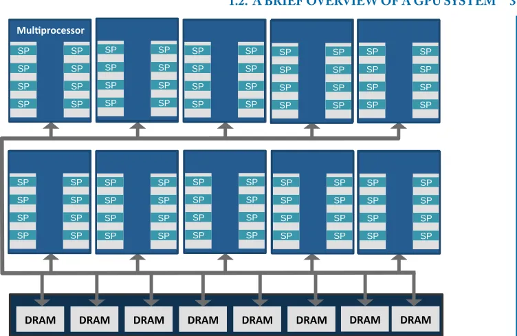
Figure1.2 illustrates the major components of a general-purpose graphics processor, based on a simplified diagram of G80. At a high level, the GPU architecture consists of several streaming
multiprocessors(SMs), which are connected to the GPU’s DRAM. (NVIDIA calls an SM and AMD
1.2. A BRIEF OVERVIEW OF A GPU SYSTEM 3 SP SP SP SP SP SP SP SP SP SP SP SP SP SP SP SP SP SP SP SP SP SP SP SP SP SP SP SP SP SP SP SP SP SP SP SP SP SP SP SP SP SP SP SP SP SP SP SP SP SP SP SP SP SP SP SP SP SP SP SP SP SP SP SP SP SP SP SP SP SP SP SP SP SP SP SP SP SP SP SP
Figure 1.2: Block diagram of NVIDIA’s G80 graphics processor (the components required for graphics processing are not shown).
SIMD/SIMT GPU processors supply high floating-point (FP) execution bandwidth, which is the driving force for designing graphics applications. To make efficient use of the high number of FP units, GPU architectures employ aSIMDorSIMTexecution paradigm (we explain SIMT and contrast with SIMD in Chapter1.3.4.) In SIMD, one instruction operates on multiple data (i.e., only one instruction is fetched, decoded, and scheduled but on multiple data operands). Depending on the word width, anywhere from 32, 64, or 128 FP operations may be performed by a single instruction on current systems. This technique significantly increases system throughput and also improves its energy-efficiency. This SIMD-style execution is essentially the same technique used in early vector processors. To support SIMD/vector operations, the register file should provide high bandwidth of read and write operations.
Multithreading The other important execution paradigm that GPU architectures employ is
hard-ware multithreading. As in more conventional highly multithreaded architectures, such as HEP [86],
M-Machine [35], Tera MTA [87], GPU processors use fast hardware-based context switching to tolerate long memory and operation latencies.
need to process many objects (e.g., pixels, vertices, polygons) simultaneously. Multithreading is the key to understanding the performance behavior of GPGPU applications. In conventional CPU systems, thread context switching is relatively much more expensive: all program states, such as PC (program counter), architectural registers, and stack information, need to be stored by the operating system in memory. However, in GPUs, the cost of thread switching is much lower due to native hardware support of such process. Although modern CPUs also implement hardware multithreading (e.g., Intel’s hyperthreading), thus far the degree of multithreading (the number of simultaneous hardware thread contexts) is much lower in CPUs than in GPUs (e.g., two hyperthreads vs. hundreds of GPU threads).
To support multithreading in hardware, a processor must maintain a large number of registers, PC registers, and memory operation buffers. Having a large register file is especially critical. For example, the G80 architecture has a 16 KB first-level software managed cache (shared memory) while having a 32 KB register file. This large register file reduces the cost of context switch between threads. This fact is a key distinction from conventional CPU architectures. We discuss these and other architecture features in more detail later in this chapter.
1.3
A GPGPU PROGRAMMING MODEL: CUDA
This section briefly discusses the CUDA programming model. The reader should refer to the latest official CUDA programming Guide for more details [73]. Part of the following explanation is adopted from an article by Hwu and Kirk [31].
1.3.1 KERNELS
NVIDIA’s CUDA (Compute Unified Device Architecture) programming interface is a C/C++ API for GPGPU programming. CUDA programs contain code that runs on a host (typically, the primary CPU processor) and kernels that run on devices (the GPU co-processor).
CUDA source code has a mixture of bothhost codethat runs on the CPUs and device code
that runs on the GPUs. The device code is also typically called as a kernel function. The host code is compiled using the standard compiler; the device code is first converted to an intermediate device language called PTX, which enables the first round of code optimizations. Later, this PTX representation is translated into a device-specific binary code, which encapsulates optimizations targeting a specific GPU. Figure1.3 shows an overview of the compilation process of a CUDA program.
1.3. A GPGPU PROGRAMMING MODEL: CUDA 5
$%
' (
Host Code Device Code (PTX)
#"))
"" $ '
Figure 1.3: Overview of the compilation process of a CUDA program (courtesy of Kirk&Hwu’s book [31]).
CPU Serial Code
. . .
. . . Device Parallel Kernel
KernelA<<< nBlk, nTid >>>(args);
CPU Serial Code
Device Parallel Kernel KernelB<<< nBlk, nTid >>>(args);
Figure 1.4: Execution of a CUDA program (courtesy of NVIDIA [72]).
another kernel, it invokes the GPU computation again. This example shows a simplified model where the CPU execution and the GPU execution do not overlap. Many heterogeneous computer applications, including newer CUDA programming models, can overlap computations between CPUs and GPUs and even overlap GPU kernel executions.
1.3.2 THREAD HIERARCHY IN CUDA
The CUDA programming model uses a three-level execution hierarchy consisting ofthreads,blocks
(orthread blocks), andgrids. The smallest work unit is a thread. Threads may be grouped into blocks
it does so on a grid, which is one or more thread blocks. This execution hierarchy is strongly coupled with (1) memory space, (2) synchronization, and (3) dispatch and retirement granularity. In real hardware, threads are executed as a lock step forming another execution unit, which is called
warp.(Warps in NVIDIA terminology and wavefront in AMD terminology.) The concept of warp is discussed in Chapter1.4.1.
When the kernel,funcKernel <<< dimGrid, dimBlock >>>(args) funckernel() is invoked, there is a totaldimGridnumber of blocks and each block has adimBlocknumber of threads. Hence, in total adimGrid×dimBlocknumber of threads executes the same kernel.
Execution of threads/blocks
All threads in a block run concurrently. Here, concurrent execution does not mean all threads are executed every single cycle. Rather, it means that all threads in a block have an active state1and are executed in a time-multiplexed fashion.
Figure 1.5: CUDA: bulk synchronization programming model (courtesy of [72]).
Hence, a thread block is the minimum dispatch and retirement unit. All threads in a block are dispatched together and when all threads in the block are completed, the block can retire. Currently, once a block is assigned a streaming multiprocessor (SM), it cannot be migrated to another SM. All threads in a thread block execute asynchronously until they reach a barrier. Hence, the CUDA programming model is an instance of the bulk-synchronous parallel programming model [33,91]. In this model, as shown in Figure1.5, programmers use barriers to synchronize all the threads. However,
1There are some exceptional cases in which some threads might have terminated earlier than others. But mostly all threads are
1.3. A GPGPU PROGRAMMING MODEL: CUDA 7
there is no mechanism to synchronize across all the blocks, since not all blocks are executed in the hardware at the same time. A block can begin execution only when there are enough resources, such as registers, for executing a block. In a given time, the number of running blocks is dependent on the resource requirement from a program and the available hardware resource. When all blocks are finished, a kernel can finish. Hence, there is an implicit barrier between kernels.
The CUDA programming model does not specify the execution order among blocks. In a given time, any number of blocks may be executing on the hardware. This flexibility enables scalable implementation of the hardware as shown in Figure1.6. Depending on the machine’s resources, different number of blocks are executed at the same time. In a low-cost system as in Figure 1.6 (left), only two blocks are executed together; on a current high-end system, up to four blocks may be executing. Currently, blocks are scheduled by drivers. There is no specific mapping between blocks and cores.
Device
Block 0 Block 1
Block 2 Block 3
Block 4 Block 5
Block 6 Block 7
Kernel grid Block 0 Block 1 Block 2 Block 3 Block 4 Block 5 Block 6 Block 7
Device
Block 0 Block 1 Block 2 Block 3
Block 4 Block 5 Block 6 Block 7
Each block can execute in any order relative to other blocks.
time
Figure 1.6: CUDA block execution patterns (courtesy of [72]).
1.3.3 MEMORY HIERARCHY
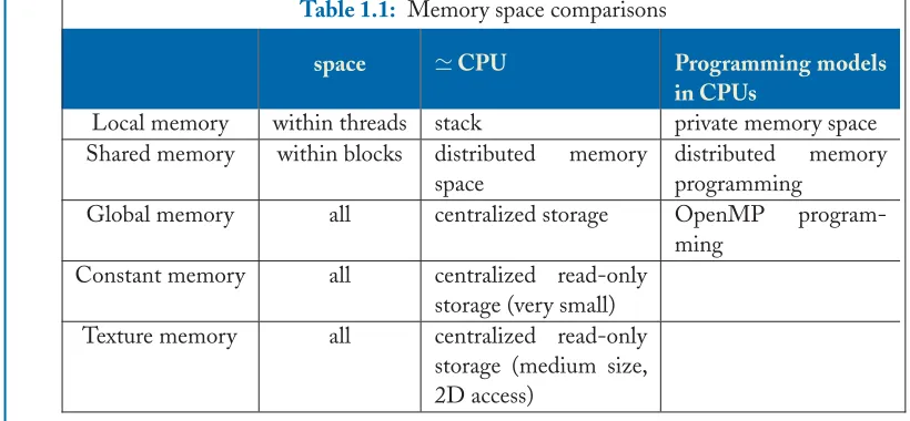
The execution hierarchy is also associated with a memory hierarchy. First, each thread has its own private registers. For memory, a thread has its own memory space, which is called the local memory. A block also has its own memory space, which is called the shared memory. All threads in a block can access the same shared memory, while threads in other blocks cannot. The entire kernel also has its own memory space, which is called the global memory. This memory is so-named because any thread in any block may access the global memory space. Table1.1summarizes the various memory spaces and their relation to the execution hierarchy.
There are also constant memory and texture memory spaces, which are similar to global memory in the sense that all threads and blocks may access them. However, these memories are specialized for graphics applications. The texture memory is used to store texture data (2D, 3D data) and the constant memory is used to store a very small number of constant variables. Both texture memory and constant memory are read only from the device side. Only the host processor can write data in these two memory spaces.
Table 1.1: Memory space comparisons
space CPU Programming models
in CPUs
Local memory within threads stack private memory space Shared memory within blocks distributed memory
space
distributed memory programming
Global memory all centralized storage OpenMP program-ming
Constant memory all centralized read-only storage (very small) Texture memory all centralized read-only
storage (medium size, 2D access)
Table1.1also compares traditional parallel programming paradigms. Accessing the shared memory space is very similar to that in the distributed memory (MPI) programming model. Between shared memory regions owned by different blocks, the CUDA program explicitly copies data through the global memory space. However, in the global memory space, all threads can access the space so the CUDA program is in this way similar to the OpenMP programming model.
1.3.4 SIMT EXECUTION
At a high level, the GPU programming model is based on the Single Program Multiple Data (SPMD) model; a kernel function defines the program that is executed by each of the thousands of fine-grained threads that compose a GPU application. Figure1.11shows that all threads execute the same kernel but all access different memory locations.
Since the programming model is SPMD, most of the threads perform the same work. Hence, a group of threads are executed in a lock-step fashion, executing the same instruction (on different data). This microarchitectural grouping of threads, which can affect both control flow and memory access efficiency, introduces the concept ofwarp—a group of threads that are executed together in a lock step.
1.3. A GPGPU PROGRAMMING MODEL: CUDA 9
if (threadIdx.x>0) { // do work
}
(a) if statement
if (threadIdx.x%2) { // divergent branch //do work 1
} else {
// do work 2 }
(b) if-else statement
Figure 1.7: Examples of divergent branches.
1.3.5 CUDA LANGUAGE EXTENSIONS
CUDA extends the C function declaration syntax. The use of these keywords is summarized in Table1.2. Using one of__global__,__device__, or__host__, a CUDA programmer can instruct the compiler to generate a kernel function, a device function or a host function. A host function is simply a traditional C function that executes on host and can only be called from another host function. By default, all functions in a CUDA program are host functions if they do not have any of the CUDA keywords in their declaration.
Table 1.2: CUDA C keywords for function declaration
Executed on the Only callable from the
__device__ float DeviceFunc() device device __global__ void KernelFunc() device host
__host__ float HostFunc() host host
1.3.6 VECTOR ADDITION EXAMPLE
We show an example of a kernel invocation using a vector addition. First, we show a traditional C program for a vector addition (C = A+ B) in Figure1.8. The actual vector addition operation is performed by aforloop. Now, the same code is changed to perform vector addition in the device (GPU). Figure1.9shows only thehostside of the code that will launch the GPU code. Figure1.10 shows thedevice(GPU) side of the code.
// compute vector sum C=A+B
void vecAdd(float *A, float *B, float *C, int n) { for (int ii = 0; ii < n; ii++) C[ii] = A[ii] +B[ii]; }
int main() {
// memory allocation for h_A, h_B, and h_C
// I/O to read h_A and h_B, N element each ...
vecAdd(h_A, h_B, h_C, N); }
Figure 1.8: A simplified traditional vector addition C code example.
# include <cuda.h> ...
void vecAdd(float *A, float *B, float *C, int n) { // memory allocation for h_A, h_B, and h_C // I/O to read h_A and h_B, N element each
...
// 1. Allocate device memory for A, B, and C // Copy A and B to device memory
// 2. Kernel launch code
// the device performs the actual vector addition
// 3. Copy C from the device memory // Free device memory
}
Figure 1.9: vecAdd function on the CPU side that calls a GPU kernel.
// Each thread performs one pair-wise addition __global__ void vecAddKernel (float *A, float *B, float *C, int n) {
int idx = threadIdx.x + blockDim.x*blockIdx.x; c[idx] = A[idx] + B[idx]; }
1.3. A GPGPU PROGRAMMING MODEL: CUDA 11
! " # $ % !
! " # $ % !
' ' ' '
' ' ' ' !"#
' ' ' '$%
' ' ' ' !
& & & &
'&
'& '& '& '& '& '& '&
Figure 1.11: All threads in a grid execute the same kernel code but access different memory locations.
(Here,blockDim.xhas the value of 4.)
Device and Global Memory
In CUDA, the host and device have separate memory spaces.2The actual hardware also has separate physical memories as shown in Figure1.1: CPUs have their own DRAM and GPUs also have their own DRAM. The GPU’s DRAM memory space is calledglobal memoryordevice memory. In order to execute a kernel on a device, the programmer needs to allocate global memory on the device and transfer pertinent data from the host memory to the allocated device memory. This corresponds to Part 1 in Figure1.9. Similarly, after a kernel execution, the programmer needs to transfer result data from the device memory back to the host memory and free up the device memory that is no longer needed (Part 3 in Figure1.9).The CUDA runtime system provides API functions for managing data in the device memory. For example, Part 1 and Part 3 of the vecAdd() function in Figure1.9need to use these API functions to allocate device memory, transfer data from device/host to host/device, and free the device memory.
Memory Data Indexing
In the SPMD programming model, a single program handles multiple data (SIMD or SIMT). Each thread operates different data. It either accesses its own register files or different memory locations.When accessing memory, a programmer or algorithm designer typically expects a particular assignment of threads to data. To specify such mappings, CUDA provides built-in variables for identifying threads, as discussed above. Figure1.11illustrates this concept for vector addition. Here, suppose we wish to add two vectors of length 16, and we wish to assign 1 thread to perform each addition. Further, suppose we create a pool of 16 threads, organized into 4 thread blocks with 4 threads each. Each thread can discover its unique thread block ID using the built-in variable
blockIdx.x, and its unique thread ID within its block using the variablethreadIdx.x, as shown in Figure1.11. From these, we can easily translate the loop iteration variable in the sequential code into an index for use in the threaded code. Also note the.xfield notation; as it happens, there are also.yand.zfields, which may be used when the most natural way to organize threads is two- or three-dimensional, as commonly occurs in imaging and graphics applications.
1.3.7 PTX
PTX is the virtual ISA used by NVIDIA GPU architectures. A compiler converts PTX code into the native ISA for a given GPU architecture. Register allocation and specific architecture-based optimizations are performed during the code generation from PTX to the native binaries.
1.3.8 CONSISTENCY MODEL AND SPECIAL MEMORY OPERATIONS
The CUDA programming model does not specify a consistency model. Since the execution model is bulk synchronous, the memory operations across threads can be reordered. One may regard the CUDA memory model as being one of weak consistency. To enforce a memory ordering, recent versions of the CUDA programming model provide built-in functions for fences, e.g., _threadfence() and mem_fence(). These functions guarantee that all the previous memory requests prior to these functions are visible to all threads. In other words, _threadfence() is used to halt the current thread until all previous writes to shared and global memory are visible by other threads.3The CUDA programming model also provides several atomic operations that are useful for implementing lock operations. Examples of atomic functions are (atomic add/sub/exchange/inc/dec/min/max).
Often atomic operations and fence() functions are used together. For example: 1. store data
2. _threadfence() 3. atomically mark a flag
These steps guarantee that if other block sees the flag, it will also see the data.4
1.3.9 IEEE FLOATING-POINT SUPPORT
Earlier GPU designs did not follow the IEEE floating-point standard, as these were not deemed as being necessary for graphics applications. However, with the rise of GPGPU programming, the floating-point implementations have increased in compliance with the IEEE-754 standard, including single-precision support in G80 architectures as well as double-precision support in the Fermi architecture.
3http://stackoverflow.com/questions/11570789/cuda-threadfence
1.4. GPU ARCHITECTURE 13
1.3.10 EXECUTION MODEL OF OPENCL
Although our discussion thus far has focused on CUDA, a consortium has assembled an alternative open-standard called OpenCL (Open Computing Language). OpenCL adopts CUDA-like con-structions but promises portability across a range of platforms, including NVIDIA GPUs, AMD GPUs, and multicore CPUs from several vendors. Applications written in OpenCL are compiled for the specific target architecture at runtime. The goal of the OpenCL consortium is to develop an industry-wide standard parallel programming environment and enable running a single application code on different types of devices and/or creating kernels from a single application and dispatching them to the available OpenCL-compatible computing devices at runtime. While CUDA is mainly built based on a fine-grained SPMD (Single Program Multiple Data) execution model with limited inter-thread communication, OpenCL also supports the task-parallel programming model. The OpenCL API provides data structures and routines to synchronize execution and share data among kernels running on different devices.
As with CUDA, an application or aprogrampartly consists of a number of functions orkernels, which are executed on OpenCLdevices. The host code assigns kernels to the available computing devices through acommand queue. To do so, the programmer needs to set up an OpenCLcontexton the host side to handle memory allocation, data transfer between memory objects, and command queue creation for devices.
Table 1.3: CUDA vs. OpenCL
OpenCL CUDA
Execution model Work-groups/work-items Block/thread
Memory model Global/constant/local/private Global/constant/shared/local + Texture
Memory consistency Weak consistency Weak consistency Synchronization Using a work-group barrier
(be-tween work-items)
Calling __sync_threads() be-tween threads
1.4
GPU ARCHITECTURE
This section sketches the design of current GPU architectures. Much of this discussion pertains to NVIDIA’s Tesla/Fermi architectures. However, our descriptions are not intended to correspond directly to any existing industrial product.
1.4.1 GPU PIPELINE
"
% &
% &
!
# $
#
$
Figure 1.12: An overview of GPU streaming multiprocessor pipeline.
Fetch and Decode Stage
1.4. GPU ARCHITECTURE 15
fetches instructions from one warp until a certain event occurs such as I-cache miss or fetching a branch instruction or an instruction buffer full. Since the front-end has multiple warps to fetch, when it encounters such events, it simply switches to fetch another warp. For the same reason, branch predictors play a diminished role and are not typically implemented. Newer GPUs execute multiple warps at one cycle, so the front-end could fetch instructions from different warps at the same cycle instead of one warp at one cycle.
After an instruction is fetched, it is decoded in the decode stage.The streaming multiprocessor can have an instruction buffer for each warp or share a buffer for all warps.
Scheduler and Score Boarding
The GPU processor has an in-order scheduler. In the G80 architecture, it executes only one warp at a time; later architectures like Fermi schedule multiple warps. The scheduler uses a scoreboard to find a ready warp. So far, no GPU architectures have employed out-of-order schedulers. However, the scheduler can select any warps that are ready. Hence, from a programmer’s view point, a program might look like an out-of-order execution. For example, the scenario in Figure1.13is possible.
Figure 1.13: An example of static and dynamic instruction traces.
same warp can be executed even if earlier instructions have not finished yet. This approach increases instruction/memory-level parallelism.
Register read/write
To accommodate a relatively large number of active threads, the GPU processor maintains a large number of register files. For example, if a processor supports 128 threads and each thread uses 64 registers, in total 128×64 registers are needed. As a result, the G80 has a 64 KB register file and the Fermi supports 128 KB of register file storage per streaming multiprocessors (in total, a 2 MB register file). The register file should have a high capacity and also high bandwidth. If a GPU has 1 Tflop/s peak performance and each FP operation needs at least two register reads and one register write, 2 T*32 B/s=64 TB/s register read bandwidth is required. Providing such high bandwidth is particularly challenging, so several techniques have been used, including multiple banks and operand buffer/collectors.
! "
!
"
Figure 1.14: GPU register file accesses. Left: using multiple banks (figure courtesy of [70]); right: using operand buffering (figure courtesy of [41]).
Multiple banks The streaming multiprocessor provides high bandwidth by subdividing the register file into multiple banks. Figure1.14shows the register file structure. All threads in the warp read the register value in parallel from the register file indexed by both warp ID and register ID [70]. Then, these register values are directly fed into the SIMD backend of the pipeline. (Please remember that each SIMD unit/lane is used by only one thread.)
1.4. GPU ARCHITECTURE 17
reading all the necessary register values right before the values are needed, which gives a very high pressure to the register file read/write ports, the processor can buffer the register values.
The buffer can store register values that are read through multiple cycles, thereby reducing the register read bandwidth requirement. In their design, four SIMT lanes form a cluster. Each entry in the streaming multiprocessor’s main register file is 128 bits wide, with 32 bits allocated to the same-named register for threads in each of the four SIMT lanes in the cluster. Several documents [13,57,63] indicate that they employ operand collector buffers.These operand collectors are also used to aggregate result values. The operand collector works as a result queue, which buffers the output from functional units before being written back into the register file. Although the main benefit of the result queues is to increase the effective write throughputs, it also provides further optimization opportunities. When the outcomes of instructions are used only in the instructions dynamically scheduled close enough, the output values can be forwarded to the input of the next operation. This behaves just like a CPU’s forwarding network [57].
When an instruction requires multiple accesses to the same bank, the register values are read over multiple cycles. Since the register addresses are determined statically, the compiler can in principle reduce or remove bank conflicts.
Figure 1.15: Detailed diagram of Operand Collector [13].
Execution stage
In the execution stage, an instruction accesses either the memory unit or functional units. The memory system is discussed in Section1.4.3.
The execution stage consists of vector processing units (AMD GPUs have a scalar unit as well). One vector lane executes one thread, which is called a stream processor in NVIDIA’s terminology. The simplest design would be to have the number of lanes and the warp size be the same. However, this approach could also require a relatively large amount of static power consumption and a large area. Instead, GPUs execute the same instruction over multiple cycles. For example, the G80 has only 8 vector lanes, and therefore the streaming multiprocessor takes four cycles to execute 32 threads (i.e., one warp). The computed results are temporarily stored and then written back to the register file together.
Back-to-back operation The execution width of GPU is wide (32 threads), which makes it much harder to have a data forwarding path. For example, 32×32 B (total 1 KB) or 32 ×64 B (total 2 KB) widths are quite large. Hence, the results are either written directly to the register file or temporarily stored in a small buffer and then written back to the register file over multiple cycles. In either case, the results are not available to dependent instructions immediately after execution. This scenario is quite different from many modern CPUs, where data forwarding is used widely. When there is a forwarding path, register read/write cycles are not in the critical path and any back-to-back operations are executed immediately following the execution latency. However, GPUs can avoid this penalty by utilizing thread-level parallelism (TLP). The pipeline simply schedules instructions from other warps so it can hide the latency. When there is enough TLP, the execution and register write latency can be hidden.
Volkov discussed this issue in his GTC’10 talk [95].When there are four threads, the streaming multiprocessor can simply switch to other threads so the execution latency can be hidden. However, when there is only one thread, these back-to-back operations take much longer. This performance issue is also discussed in Chapter4.1.
1.4. GPU ARCHITECTURE 19
1.4.2 HANDLING BRANCH INSTRUCTIONS
Branches are particularly challenging to implement well in GPUs. Recall that current GPU hardware implementations fetch just one instruction for each warp.When this instruction is a divergent branch, threads within a warp will need to execute different instruction paths. This challenge is common to GPUs and earlier vector processors.
The solution in vector processors is to use vector lane masking or predication [17,81]. However, the problem in GPUs is slightly different. Not only does part of the SIMD unit need to be predicated, but the processor also needs to fetch instructions from different paths. Indeed, the existence of divergent branch is the major difference between SIMD and SIMT execution. Fung et al. first described this problem in GPGPUs [38].
Figure1.16illustrates the problem. Suppose that the warp size is 4 and that 2 threads take the taken path while the remaining 2 threads go to the fall-through path. The streaming multiprocessor has to fetch both paths one by one. An active mask indicates which threads participate in each path. The active mask bit information is also used in any register read or write.
if (threadx.Idx < 2) { // do work 1 }
else {
// do work 2 }
Figure 1.16: Divergent branch example.
The most naïve solution is SIMD serialization. When divergence occurs at a given PC, the processor serializes the threads within a warp. This will cause performance degradation.
A stack-based reconvergence solution is proposed to handle divergent branches [38,39,62, 100]. In their scheme, divergent threads executewithoutlock-step until the end of the program; the processor detects the point at which the threads can rejoin in a lock-step again, i.e., when they may form a warp again.The control-flow reconvergence point is the point where all threads merge. When a program diverges, the processor inserts the reconvergence point into the stack. When threads in one path reach the reconvergence point, the processor fetches instructions from other remaining paths. Once all the divergent paths are fetched, in other words once all threads reach their reconvergence points, the divergent threads merge.
.... .... .-.. -.--.-.. -.--... .... $ ) ) ) ) % +, % # ) !$).... $ $
+, !$ &#
+,!
# ) !$).-.. $
!$ &#
+,&#! -.--.... $ ' ' # ) !$)-.--$
!$ &#
+,&#! .... ' # ) !$).... $
!$ &#
+,&#!
Figure 1.17: A stack-based divergent branch handling mechanism (figure courtesy of [38,70]).
Each stack entry has three fields: the PC address of the reconvergence point, active mask bits, and the next PC address. Figure1.17illustrates the process [38,70]. Figure1.17(a) shows a control flow graph. Figure1.17(b) shows an initial state of the stack. When a processor fetches a divergent branch, it pushes a join entry in the stack. Then, the processor chooses one of the path and it pushes the other path information in the stack. The active mask field is set to the current active mask. (Figure1.17(c) shows the stack after executing branch A.) The top of the stack shows the join entry and active mask of the path. When a processor fetches an instruction, it always checks whether the next PC address matches with the reconvergence PC. After fetching PC B, the next PC address is D, which is the same value in the top of the stack. Hence, the processor pops the top entry from the stack and starts to fetch from PC C and uses the active masks in the entry. (Figure1.17(d) shows the state of the stack after executing PC B.) Since the next PC address is again D, the top entry in the stack is popped. The active mask is all 1s, so now all threads are participating the path. (Figure1.17(e) shows the state after executing PC C).
1.4. GPU ARCHITECTURE 21
In divergent memory operations, some threads hit the cache but some do not so threads generate different memory latencies within a warp. Several other solutions such as dynamically changing the execution units such as thread compaction [40], large warp formation [70], compaction based on the benefit prediction [79], and interweaving threads [20,32] at dynamic time are also proposed.
Solutions to reduce the impact of divergent branches in software Several compiler-based solutions also exist. Zhang et al. reduce divergent branches by remapping data locations [105]. Han and Adelrahman propose compiler solutions [46]. Diamos et al. rearrange threads based on the frequency at static time [32]. Their solutions can also reduce the divergent branches.
1.4.3 GPU MEMORY SYSTEMS
The GPU memory system has several levels of hierarchy. Because there can be a large number of memory requests on-the-fly, the system requires several large buffers and/or queues.
A streaming multiprocessor has a cache to supply fast data accesses. In earlier GPGPU ar-chitecture like the G80, there were only software-managed first-level caches. More recent GPGPU architectures adopt a more aggressive cache hierarchy. In Fermi, the first-level cache can be con-trolled only by software (program) or in a hybrid software-hardware managed fashion. If a program controls a software managed cache, the instruction explicitly brings data to the cache and evicts it. The shared memory space in CUDA is explicitly controlled by software. Since memory addresses are determined at run-time, unlike register files, there could be bank conflicts in the cache.
Table 1.4: Memory space and hardware access time [82,98]
Memory Space Tesla Fermi access latency
Local memory DRAM DRAM and hardware cache
100s cycles
Shared memory Software cache Software cache 4 – 32 cycles Global memory DRAM DRAM and hardware
cache
100s cycles
Constant memory DRAM and con-stant cache
DRAM and constant cache
100s cycles or 4 cycles (cache hit)
Texture memory DRAM and texture cache
DRAM and texture cache
100s cycles or 4 cycles (cache hit)
Table 1.4 shows different memory spaces and typical memory latencies. So far, computer architects have presented two major problems in the memory system. One is managing the large size of buffers, and the other is dealing with long memory latency.
of DRAM banks to increase the bandwidth even further. Typically, GDDRs provide higher DRAM bandwidth than DDR, because of the wider burst length and DRAMs are directly connected to pro-cessors. In CPUs, DRAMs are connected through DIMMS which slows down the communication bandwidth
DRAM scheduling algorithms are tuned to provide high bandwidth. FRFCFS is the best way to increase throughput oriented computing. Since GPGPU applications have high spatial locality, FRFCFS shows much higher performance than FCFS [103].
Figure 1.18: Coalesced uncoalesced memory requests. Left: all threads are accessing sequential mem-ory addresses (coalesced); right: threads are accessing non-sequential memmem-ory addresses (uncoalesced): courtesy of [72].
Multiple memory transactions The basis of SIMD execution unit is executing multiple data at once. If the data is in the register, all the register files can be accessed together. The challenges result when a warp executes memory operations. The memory addresses can be anywhere. In earlier GPUs, this was one of the most important performance optimizations [82,83,96]. When all threads within a warp access sequential memory addresses, these memory addresses can be easily represented by a few transactions. However, if memory addresses are all scattered, these memory operations will generate multiple transactions. In earlier GPUs, especially earlier than CUDA computing version 1.2, these were called coalesced and uncoalesced memory addresses as shown in Figure1.18. Coalesced memory addresses generate one to four memory transactions depending on the transaction sizes and uncoalesced memory addresses generate up to 32 transactions. After some hardware optimizations, the hardware combines as many memory addresses as possible and generate fewer transactions. Coalescing is used to combine as many requests as possible. Still reducing the number of memory transactions is one of the essential performance optimizations. The hardware typically has a special hardware unit to handle this scatter/gather operation.
1.5. OTHER GPU ARCHITECTURES 23
CC MMMMM CC CC MMMMMD
W0
C MMMMM CC CC MMMM D
W1
Context Switch
D
D
D
CC
Co
Memory Request Memory Request Memory Request
Memory Request Memory Request
Memory Request Memory Request
Memory Request
Figure 1.19: Multiple in-flight memory requests (even though 2 warps are running, 4 memory requests are concurrently serviced).
this can increase the number of in-flight memory requests. When a program has high TLP, this does not affect too much. However, when there are fewer threads, exploiting MLP effects can increase the total MLP significantly.
1.5
OTHER GPU ARCHITECTURES
1.5.1 THE FERMI ARCHITECTURE
Major successors to the G80 design are based on the Fermi architecture, which was first released in 2010. The Fermi architecture has taken a significant leap forward in GPU architecture design by providing a two-level cache hierarchy to better support the applications that are not able to use the GPU’s shared memory efficiently. Among other major improvements are the improved double precision performance, faster atomic operations to reduce the cost of inter-thread-block communication, and the error correction code (ECC) support. A more detailed description of the hardware and software features of the Fermi architecture can be found in [51].
1.5.2 THE AMD ARCHITECTURE
ATI stream technology which is supported by all modern AMD GPUs such as ATI Radeon and Fire-Stream has also provided massively parallel computation. ATI originally had supported Brook+[3] to provide GPGPU features, but instead ATI now supports OpenCL. So far the major difference between NVIDIA’s GPU architectures and AMD’s GPU architectures is that AMD has a SIMD-VLIW architecture. Four ALUs and one branch or five ALUs and one branch unit are packed together, all of which execute the same instruction. AMD can easily support scalar instructions as one of the VLIW units but NVIDIA so far only has vector units.
low-end GPUs are integrated in the fusion architecture so the AMD fusion architecture has not yet been widely used for GPGPU computing. Nonetheless, we predict that soon AMD’s architecture will be widely used as GPGPU computing platforms.
1.5.3 MANY INTEGRATED CORE ARCHITECTURE
Intel’s Many Integrated Core (MIC) architecture also targets high-throughput computing proces-sors [26]. Unlike AMD and NVIDIA, Intel’s MIC architecture executes native x86 ISAs, which is the greatest strength of Intel’s platforms. MIC also has a wide SIMD unit (512 bits wide) to produce high-throughput computing, but it also has most of the features that are traditionally avail-able in CPU architectures, such as virtual memory, fully coherent cache, and a branch predictor. However, the number of concurrently running threads is much smaller (4) than that of NVIDIA or AMD. Hence, MIC is not only specialized for throughput oriented computing, but also targets latency-limited applications.
1.5.4 COMBINING CPUS AND GPUS ON THE SAME DIE
25
C H A P T E R 2
Performance Principles
Developing algorithms for GPGPUs is fundamentally about applying the same long-studied prin-ciples of parallelization and I/O-efficient design relevant to other shared memory parallel platforms. This chapter reviews these principles, focusing on recent results in both the theory and practice of parallel algorithms, and suggests a connection to GPGPU platforms. Ideally, applying these princi-ples with the right cost models leads not only to provably efficient algorithms, but also offers hints to architects about the features and configurations likely to have the most impact on the performance of a given computation. Thus, we believe this discussion will be useful to practitioners in various aspects of parallel computing, not just those interested specifically in GPGPUs.
2.1
THEORY: ALGORITHM DESIGN MODELS OVERVIEW
The two most important characteristics of any algorithm likely to determine its performance are: (a) how much parallelism is available and (b) how much data must move through the memory hierarchy. Thus, when designing an algorithm, we would like an abstract machine model that allows us to assess our algorithm along these dimensions. In such a model, we might want to do the same kind of “big-O” analysis to which we are accustomed in the sequential case. Doing so would allow us to get the high-level algorithm design right before moving on to lower-level performance optimization and tuning. Importantly, the abstractions should not be so cumbersome that we cannot in a reasonable amount of time design and analyze candidate algorithms.
Although the state of algorithm design models is in flux, we have reasonable options. For GPGPUs and other manycore-style processors, two suitable models are the so-calledwork-depth(or
work-span) model for analyzing parallelism [15,28,54], and theexternal memory modelfor analyzing
I/O behavior in the presence of a memory hierarchy [4,93,94].These two models evolved separately, but recent work has shown ways in which to connect them [16,30]. The remainder of this chapter reviews aspects of this work.
2.2
CHARACTERIZING PARALLELISM: THE WORK-DEPTH
MODEL
In the work-depth model, we represent a computation by a directed acyclic graph (DAG) of opera-tions, where edges indicate dependencies, as illustrated in Figure2.1. Given the DAG, we measure itswork,W (n), which is the total number of unit-cost operations for an input of sizen, and its
1
2
3
D(n)
…
D
(
n
)
W
(
n
)
= total nodes
= critical path
Figure 2.1: A parallel computation in the work-depth (or work-span) model. The computation for an
input of sizen is a directed acyclic graph withW (n) nodes, each representing a unit-cost operation;
edges representing strict dependencies among these operations; and a critical path of lengthD(n)nodes.
Our goal is to design algorithms that achievework-optimality while maximizing the average available
2.2. CHARACTERIZING PARALLELISM: THE WORK-DEPTH MODEL 27
thatD(n)ought to be a lower bound on the minimum execution time, and the ratioW (n)/D(n)
effectively measures the average amount of available parallelism as each critical path node executes. In fact, the ratioD(n)/W (n)is similar to the concept of a sequential fraction, as one might use in evaluating Amdahl’s Law [7,47,99]. Thus, our implicit goal is to maximizeW (n)/D(n), or, alter-natively, minimizeD(n)/W (n). Importantly, this model makes no explicit reference to the number of processors. In this sense, we may regard the model as being machine-independent. Nevertheless, if we want to know how many processors to throw at an algorithm,W (n)/D(n)is a suitable guide. However, it is easy to maximizeW (n)/D(n)and still get a bad algorithm. For instance, we can artificially inflate the total operationsW (n). Thus, we should also try to ensure our algorithm is
work-optimal, a property which says thatW (n)is not asymptotically worse than the best sequential
algorithm. Indeed, work-optimality is a critical requirement.
Let’s see why work-optimality matters. First, note that it is possible to estimate (crudely) the algorithm’s running time givenpidentical processors, using a theorem by Brent [19]. This theorem says that if the nodes of the DAG have unit cost and the machine haspprocessors, then it is possible to schedule the DAG so that the time to execute (compute) the DAG,Tcomp(n;p), is
Tcomp(n;p)=D(n)+
W (n)−D(n)
p . (2.1)
Suppose we have designed a highly parallel algorithm, with W (n)p·D(n), and furthermore that our algorithm only exceeds the workW0(n) of the best sequential algorithm by a factor of
(n), i.e.,W (n)=W0(n)·(n). Then, the speedup of our algorithm onp processors is roughly
W0(n)/(W (n)/p)=p/(n).That is, the best possible speedup ofpwill be reduced by(n). Consider
the relatively small factor of(n)=logn. Even forn=1024,logn=10, meaning the best possible speedup is an order of magnitude less than we might hope for. Put another way, to even match
the sequential algorithm, we needp > (n). Thus, if we are deciding between anO(n)sequential algorithm and anO(n2/p)parallel algorithm, we will needp=njust to match the sequential case. These examples underscore the importance of work-optimal algorithms.
Example: Reduction. Suppose we wish to compute the sum ofnvalues. A sequential algorithm would lead to a DAG like the one shown in Figure2.2. In this case, we perform(n)operations but the critical path is also of length(n).Thus, the available parallelism—-or ratio ofW (n)/D(n)—-is a constant: no matter how large the input, there is never more than a fixed amount of concurrency.
An algorithm with more parallelism might instead have the DAG shown in Figure2.3. This algorithm organizes the additions into a tree, where independent subtrees can be performed in parallel. This tree still performsW (n)=(n)total operations, and is thus work-optimal. However, the depth of this DAG is justD(n)=(logn), the height of the tree. Thus, asngrows, so does the average available parallelism, in the amount ofW (n)/D(n)=(n/logn). By this measure, this algorithm is a better one than the sequential algorithm, just as we would expect.
In the specific case of Figure2.3, wheren=16, the workW (16)=31nodes and the depth
2 3 4 n
…
1
+ + + +
W
(
n
) = Θ (
n
)
D
(
n
) = Θ (
n
)
Figure 2.2: Work-depth example: summing a list ofnelements with a sequential algorithm. Both the
work and the depth are(n), meaning the available parallelismW (n)/D(n)is a constant.
+
+ +
+ +
+
1 2 3 4
+ +
+
5 6 7 8
+ +
+
9 10 11 12
+ +
+
13 14 15 16
W
(
n
) =
O
(
n
)
D
(
n
) =
O
(log
n
)
Figure 2.3: Work-depth example: summing a list ofn=16elements with a tree algorithm.
retrieve the values.) Then,W (16)/D(16)=31/5=6.2. Thus, there are an average of≈6nodes available to be executed in parallel during the computation. This implies that we could not gainfully use more than about six “processors.”1
2.2. CHARACTERIZING PARALLELISM: THE WORK-DEPTH MODEL 29
C
(
i
,
j
)
B
(:,
j
)
A
(
i
,:)
C
←
A
×
B
c
ij
←
n
k
=1
a
ik
·
b
kj
W
(
n
)
D
(
n
)
=
O
n
3
log
n
Figure 2.4: Work-depth example: multiplying twon×nmatrices.
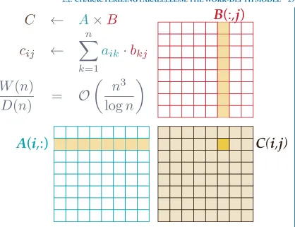
Example: Matrix multiply. Consider the multiplication of twon×nmatrices,C ←A×B, as illustrated in Figure2.4. Each output elementcij is the dot product betweenAi,:, which is rowiof
A, andB:,j, which is columnj ofB. A dot product involves an elementwise multiplication of the
vectors, followed by a sum-reduction of those results. This dot product requires(n)operations. Since there aren2elements ofC, the workW (n)=(n3).2
To computeD(n), observe that then2output elements have no dependencies among them; the only dependencies occur during the reduction to compute each output element. Thus,D(n)= (logn). The ratio ofW (n)/D(n)=(n3/logn)is asymptotically very high, and so our analysis confirms what we would expect, namely, that a matrix multiply has plenty of parallelism fo
![Figure 1.4: Execution of a CUDA program (courtesy of NVIDIA [72]).](https://thumb-us.123doks.com/thumbv2/123dok_us/586323.2057856/19.612.208.545.123.313/figure-execution-cuda-program-courtesy-nvidia.webp)
![Figure 1.5: CUDA: bulk synchronization programming model (courtesy of [72]).](https://thumb-us.123doks.com/thumbv2/123dok_us/586323.2057856/20.612.154.440.333.514/figure-cuda-bulk-synchronization-programming-model-courtesy.webp)
![Figure 1.6: CUDA block execution patterns (courtesy of [72]).](https://thumb-us.123doks.com/thumbv2/123dok_us/586323.2057856/21.612.206.453.305.394/figure-cuda-block-execution-patterns-courtesy.webp)

![Figure 1.17: A stack-based divergent branch handling mechanism (figure courtesy of [38, 70]).](https://thumb-us.123doks.com/thumbv2/123dok_us/586323.2057856/34.612.138.514.130.375/figure-stack-divergent-branch-handling-mechanism-gure-courtesy.webp)