University of New Orleans University of New Orleans
ScholarWorks@UNO
ScholarWorks@UNO
University of New Orleans Theses and
Dissertations Dissertations and Theses
Summer 8-13-2014
Transverse Thermoelectric Effect
Transverse Thermoelectric Effect
Charles Crawford [email protected]
Follow this and additional works at: https://scholarworks.uno.edu/td
Recommended Citation Recommended Citation
Crawford, Charles, "Transverse Thermoelectric Effect" (2014). University of New Orleans Theses and Dissertations. 1866.
https://scholarworks.uno.edu/td/1866
This Thesis-Restricted is protected by copyright and/or related rights. It has been brought to you by
ScholarWorks@UNO with permission from the rights-holder(s). You are free to use this Thesis-Restricted in any way that is permitted by the copyright and related rights legislation that applies to your use. For other uses you need to obtain permission from the rights-holder(s) directly, unless additional rights are indicated by a Creative Commons license in the record and/or on the work itself.
Transverse Thermoelectric Effect
A Thesis
Submitted to the Graduate Faculty of the University of New Orleans in partial fulfillment of the
requirements for the degree of
Master of Science in
Applied Physics
by
Charles Crawford
B.S. Louisiana State University in Shreveport, 2010
B.S. Louisiana State University in Shreveport, 2010
Contents
List of Figures ix
List of Tables x
Abstract xi
1 Introduction 1
2 Background 6
2.1 Transport Equations . . . 6
2.1.1 Low Field Boltzmann Transport Equation Solution . . . 6
2.1.2 Coupled Current Equations . . . 10
2.2 Using the Coupled Current Equations . . . 12
2.2.1 The General Equations . . . 12
2.2.2 Transverse Thermoelectric Geometry . . . 16
2.3 Open Circuit Eddy Currents . . . 18
3 Simulations 24
3.1 COMSOL Transverse Thermoelectric Package . . . 24
3.1.1 COMSOL Physics Builder . . . 24
3.1.2 Modifying the Thermoelectric Module . . . 25
3.2 Validation Simulations . . . 28
3.3 Transverse Seebeck Effect . . . 32
3.4 Transverse Peltier Effect . . . 35
4 Results 37 4.1 Transverse Seebeck Effect . . . 37
4.1.1 Aspect Ratio and Output Voltage . . . 37
4.1.2 Angle of Inclination and Aspect Ratio . . . 38
4.1.3 Seebeck Tensor and Potential . . . 41
4.1.4 Eddy Currents in the ASM and ILM . . . 44
4.1.5 Mathematical Difference in ILM and ASM . . . 47
4.2 Transverse Peltier Effect . . . 53
4.2.1 Peltier Aspect Ratio Comparison . . . 54
4.2.2 ASM and ILM Differences . . . 57
4.3 Device Engineering . . . 61
4.3.1 ILM . . . 61
4.3.2 ASM . . . 62
A Landauer Approach 68
A.1 Charge Current . . . 68
A.2 Heat Current . . . 72
B Computation Tables 74
B.1 Zahner et al. Validation Tables . . . 74
B.2 Kyarad et al. Validation Tables . . . 76
C List of Symbols 78
Bibliography 83
List of Figures
1.1 Schematic of a thermoelectric couple consisting of an n- and p-type
semiconductor operating in power generation mode. A source of heat
at the top drives charge carries to the cooler side, producing a current. 2
1.2 Schematic of a thermoelectric couple consisting of an n- and p-type
semiconductor operating in cooling mode. A source of current carries
heat to the bottom heat sink, cooling the top plate. . . 2
1.3 Schematic of a longitudinal thermoelectric device in power generation
mode. . . 3
1.4 Diagram of the transverse Seebeck effect simulation where a
temper-ature difference is in z-direction, and the potential difference is
calcu-lated in the x-direction. . . 5
1.5 Diagram of the transverse Peltier effect simulation where a current is
injected in the z-direction, and heat flows in z-direction to cool off the
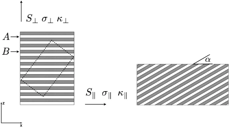
2.1 Geometry of a synthetically created anisotropic thermoelectric device
with parallel and perpendicular components of material parameters
shown. . . 16
3.1 CAD model of a device made using the isotropic layer model where
the layers are apparent. . . 26
3.2 CAD model of a device made using the anisotropic slab model where
the continuity of the geometry implies the purely mathematical nature
of the model. . . 27
3.3 Experimental set up in Zahner et al. with constant heat flux applied
to sample top and potential difference calculated from left to right. . 28
3.4 Validation of the physics modules with the data in measured in Zahner
et al. for both ILM and ASM. . . 29
3.5 Experimental set up in Kyarad et al. in which a current is injected into
the left face, and Peltier cooling occurs across the top of the device
with the bottom face kept at constant temperature. . . 30
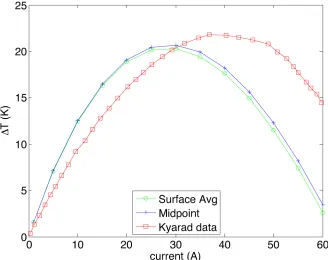
3.6 Validation of the physics modules with the data in measured in Kyarad
et al. for the ASM using the midpoint computation as well as the
surface average. . . 31
3.7 Diagram of the transverse Seebeck effect simulation where a
temper-ature difference is in z-direction, and the potential difference is
3.8 Diagram of the transverse Peltier effect simulation where a current is
injected in the z-direction, and heat flows in z-direction to cool off the
top plate. . . 35
4.1 Difference in voltage drop profile across z-axis for the ASM and ILM
in a Seebeck effect simulation. . . 38
4.2 Seebeck effect model comparison of ILM and ASM for aspect ratios
∆x/∆z = (10,5,2, .5). . . 39
4.3 Magnitude of Seebeck components, Sxz and Szz for angles of
inclina-tion 0◦-90◦. . . 42
4.4 Magnitude of voltage components contributing to x component of the
thermoelectric field for angles of inclination 0◦-90◦. . . 43
4.5 ASM (left) and ILM (right) shown with normalized eddy current
den-sities for open circuit Seebeck potential at 45 degree angle of
inclina-tion, aspect ratio of 1/2, and ten degree temperature difference top to
bottom. . . 45
4.6 ASM (left) and ILM (right) shown with normalized eddy current
den-sity for open circuit Seebeck potential at 45 degree angle of inclination,
aspect ratio of 1/1, and ten degree temperature difference top to bottom. 45
4.7 ASM normalized eddy current density for open circuit Seebeck
po-tential at 45 degree angle of inclination, aspect ratio of 2/1, and ten
4.8 ILM normalized eddy current density for open circuit Seebeck
poten-tial at 45 degree angle of inclination, aspect ratio of 2/1, and ten
degree temperature difference top to bottom. . . 46
4.9 Effect of width on the ASM for angles of inclination 0◦-90◦. . . 52
4.10 Temperature distribution across thermoelectric device CAD model of
Peltier effect for ILM and ASM. . . 53
4.11 Temperature difference created in z-direction for injected currents for
ILM and ASM for aspect ratios ∆x/∆z =(5,2,1). . . 54
4.12 Temperature difference for aspect ratio ∆x/∆z = (10,5) showing the
divergence of models at high aspect ratio. . . 55
4.13 Convergence of ILM to ASM in the limit that layer thickness goes to
zero tA→0 and tB →0. . . 56
4.14 Difference in temperature distribution across x-direction for the ASM
and ILM in a Peltier effect simulation. . . 58
4.15 Current density plots for ILM and ASM showing the extra component
in the ILM. . . 59
4.16 Zoomed in current density plot for the Peltier ILM simulation showing
extra surface perpendicular component. . . 60
4.17 Zoomed in current density plot of Peltier ASM simulation showing no
surface perpendicular component. . . 60
4.19 ILM surface plot of the potential distribution over a transverse
ther-moelectric device with heat flux applied of 137,000(W/m2) to top,
and 0V held at right side. . . 62
4.20 ASM model of a single transverse thermoelectric with heat flux applied
of 137,000(W/m2) to the top section, and 0V held at bottom right
side copper plate. . . 63
4.21 Transverse thermoelectric device linked in series with heat flux applied
of 137,000(W/m2) to the top of each section, and 0V held at bottom
right side copper plate. . . 64
A.1 A change in Fermi distribution due to an applied potential . . . 69
A.2 A change in Fermi distribution due to a change in temperature. . . . 69
A.3 A change in Fermi distribution due to a change in temperature and
List of Tables
2.1 Symbol Definitions . . . 21
B.1 Computations of ILM for the Zahner confirmation simulations to
de-termine the validity of the custom physics modules. . . 74
B.2 Computations of ASM for the Zahner confirmation simulations to
de-termine the validity of the custom physics modules. . . 75
B.3 Computations of ASM for the Kyarad confirmation simulations to
determine the validity of the custom physics modules. . . 76
B.4 Computations of ILM for the Kyarad confirmation simulations to
de-termine the validity of the custom physics modules. . . 77
Abstract
Anisotropic thermoelectric effects can be measured in certain materials. Anisotropy
can also be simulated using a repeated, layered structure of two materials cut at
an angle. Various aspect ratios and angles of inclination are investigated in device
geometry in order to maximize the thermopower. Eddy currents have been shown to
occur in thermoelectric devices, and evidence of these currents are revealed in finite
element analysis of the artificially synthesized anisotropic Peltier effect.
Keywords: thermoelectric effect, Seebeck, Peltier, thermal conductivity,
Chapter 1
Introduction
Thermoelectric effects were first discovered by Thomas Johann Seebeck around 1820.
The effect that Seebeck discovered bears his name and occurs when a temperature
difference along a block of material causes a potential difference across the block.
In 1834 the physicist Jean-Charles-Athanase Peltier found that running an electric
current through a junction of two different materials either cooled or heated the
junction depending on the direction of current into the junction [1]. This phenomenon
is similarly called the Peltier effect after its discoverer. About 20 years after Peltier’s
contributions, William Thomson (Lord Kelvin) derived a thermodynamic relation
between the Seebeck coefficient (S) and Peltier coefficient (Π), i.e. Π =S∗T, where
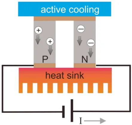
Figure 1.1: Schematic of a thermoelectric couple consisting of an n- and p-type semiconductor operating in power generation mode. A source of heat at the top drives charge carries to the cooler side, producing a current.
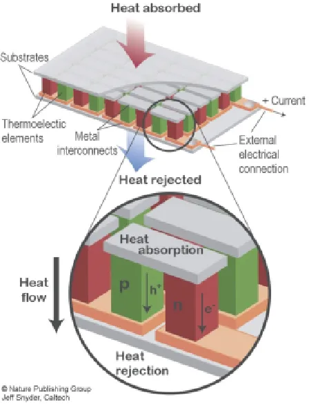
Thermoelectric modules are traditionally made using pairs of n-type (electron
conducting) and p-type (hole conducting) semiconductors. One couple (called a
unicouple) is shown schematically in Fig. 1.1 and Fig. 1.2. Figures 1.1 and 1.2
demonstrate that the thermoelectric can be used for both power generation and
solid-state cooling. In a device, many such pairs are connected electrically in series
and thermally in parallel, as shown in Fig.1.3 [3].
Figure 1.3: Schematic of a longitudinal thermoelectric device in power generation mode.
Thermoelectric research continued into the 20th century and was met with
next step in power generation, but those hopes dwindled as thermoelectric efficiency
never reached the efficiency of traditional generators. This solid state power
gener-ation has had some success since the 1940s and 1950s, however, funding has all but
disappeared, relatively speaking. The famous Voyager spacecrafts have used
longi-tudinal thermoelectrics since 1977 to power their systems, and the power is expected
to last until 2025. The loss of this power source will not only be attributed to the
breakdown of the thermoelectric materials which is minimal, but mainly due to the
radioactive decay of the plutonium heat source [4]. Other uses include everyday
ap-plications such as seat heater/coolers, small refrigerators, and camping equipment
for charging phones or GPS location devices.
The transverse thermoelectric effect has the advantage of using only one type
of doped semiconductor instead of the two as the longitudinal effect uses. Also,
the heat flow and electric current flow in perpendicular direction and, hence, are
decoupled. Figures1.4and1.5 illustrate the general geometry of both the transverse
thermoelectric effects, Seebeck power generation and Peltier cooling.
Transverse thermoelectric theory has sparked a resurgence in thermoelectric
re-search in recent years. The transverse effect has the potential to reduce the amount
of material, relative to longitudinal thermoelectrics, needed for equivalent output
power. Since the current cost of sending a pound of anything into space is $10,000,
less material for equal output will have a huge effect on the cost of spacecrafts. An
important application is the conversion of waste heat to electricity to be put back into
the grid. With the modernization of developing countries and ever increasing energy
creation is paramount.
Figure 1.4: Diagram of the transverse Seebeck effect simulation where a temperature difference is in z-direction, and the potential difference is calculated in the x-direction.
Chapter 2
Background
2.1
Transport Equations
2.1.1
Low Field Boltzmann Transport Equation Solution
For thermoelectrics we are interested in the electrical conductivity, thermal
con-ductivity, and Seebeck coefficient. These parameters are dependent on the band
structure of the solid, carrier scattering mechanisms, and carrier concentration through
the Fermi energy. These physical properties are calculated by first calculating the
distribution of electrons as a function of energy using the Boltzmann Transport
Equation (BTE). The BTE contains both the gradient of the electrochemical
po-tential (electric field) and the gradient of temperature. Both the electric field and
temperature gradient are responsible for the motion of the charge carriers.
Boltz-mann equation
∂f
∂t +v· ∇rf +F· ∇pf = ∂f
∂t
coll+s(r,p, t) (2.1)
f0 =
1
1 +e[EC(r,p)−EF]/kBT (2.2)
The relaxation time approximation is used with no source of carriers being injected
into the system. So, s(r,p, t) = 0 and ∂f∂t
coll
=−fA
τf, and fA is the function that is
being solved for. Since f0 is symmetric in momentum, the average velocity is zero.
Allowing a distribution such that a little current is flowing by thinking of the Fermi
distribution as a sum of two parts symmetricfS and anti-symmetric fA, gives
f =fS+fA (2.3)
fS =
1
1 +eΘ where Θ = [EC0(r, t) +E(p)−Fn(r, t)]/kBT(r, t) (2.4)
−fA τf
=v· ∇r(fS+fA) +F· ∇p(fS+fA). (2.5)
With the assumptions
fS fA, |∇rfS| |∇rfA|, hspace1mm|∇pfS| |∇pfA|
the equation simplifies to
−fA τf
fS ≡fS(Θ), so the product rule dictates that
∇rfS =
∂fS
∂Θ∇rΘ (2.7)
and
∇pfS =
∂fS
∂Θ∇pΘ. (2.8)
Using Eq. 2.6 and working out the derivatives ∇rΘ and ∇pΘ
−fA τf
=v· ∂fS
∂Θ∇rΘ +F·
∂fS
∂Θ∇pΘ (2.9)
∇pΘ =
∂E(p)
∂p
1
kBT
= v
kBT
(2.10)
∇rΘ =
[∇rEC0(r)− ∇rFn(r)]
kBT(r)
+ [EC0(r) +E(p)−Fn(r)]∇r
1
kBT(r)
(2.11)
−fA τf
= ∂fS
∂Θ (v· ∇rΘ− ∇rEC0· ∇pΘ) where − ∇rEC0(r) =F (2.12)
−fA τf
= ∂fS
∂Θ
v · ∇rΘ−v·
∇rEC0 kBT
(2.13)
−fA τf
= ∂fS
∂Θv·
[−∇rFn(r)]
kBT(r)
+ [EC0(r) +E(p)−Fn(r)]∇r
1
kBT(r)
Finally,
fA=
τf
kBT
−∂fS
∂Θ
v · F (2.15)
where
F =−∇rFn(r) +T[EC0(r) +E(p)−Fn(r)]∇r
1
T
(2.16)
F in Eq. 2.16 is ”interpreted as a generalized force” and does apply when
mag-netic fields are present sinceF6=−∇rEC0(r) in a magnetic field [5]. The components
are now gathered and can start being put together to build the coupled current
2.1.2
Coupled Current Equations
The equations for electric and heat current densities are, respectively [5],
J = −q Ω
X
p
vfA(p) (2.17)
JQ =
1 Ω
X
p
E(p)vfA(p) (2.18)
Equation 2.17 says that the electric current is the charge times the average velocity
of the moving charges. Equation 2.18 says that the heat flow is the energy times
the average velocity of the heat carriers. Lundstrom mentions an important point
concerning the velocity in Eq. 2.18. He states that the kinetic energy E(p) should
be the energy associated with the random motions of temperature and not the drift
energy associated with the average motion of particles in an applied field [5].
Singling out the electric current equation and plugging in our low field solution
to the Boltzmann transport equation, we have
J= −q Ω
X
p
vfA(p) (2.19)
J= −q Ω
X
p
v τf kBT
−∂fS
∂Θ
v· F (2.20)
J= −q
ΩkBT
X
p
v(v· F)τf
−∂fS
∂Θ
(2.21)
Displaying equations in indicial notation will be more revealing. This way the
equation becomes
Ji =
−q
ΩkBT
X
p
vivjFjτf
−∂fS
∂Θ
(2.22)
Ji =
−q
ΩkBT
X
p
vivj
∂j(−Fn) +T[EC0(r) +E(p)−Fn]∂j
1 T τf −∂fS
∂Θ
(2.23)
Ji =σij∂i(Fn/q) +Bij∂i(1/T) (2.24)
where
σij =
q2
ΩkBT
X
p
vivjτf(p)
−∂fS
∂Θ
(2.25)
Bij =
−q
ΩkBT
X
p
vivjτf(p)T[EC0(r) +E(p)−Fn]
−∂fS
∂Θ
(2.26)
Now, looking at the heat current equation, we have
JQ =
1 Ω
X
p
E(p)vfA(p) (2.27)
JQ =
1 Ω
X
p
[EC0(r) +E(p)−Fn(r)]v
τf
kBT
−∂fS
∂Θ
v· F (2.28)
JQ =
1 ΩkBT
X
p
v(v· F) [EC0(r) +E(p)−Fn(r)]τf(p)
−∂fS
∂Θ
Substituting in Eq. 2.16 and writing the heat current in indicial notation
JQi =wij∂j(Fn/q) +Kij∂j
1 T , (2.30) where
wij =
−q
ΩkBT
X
p
vivjτf(p)[EC0(r) +E(p)−Fn(r)]
−∂fS
∂Θ
(2.31)
Kij =
−q
ΩkB
X
p
vivjτf(p)[EC0(r) +E(p)−Fn(r)]2
−∂fS
∂Θ
(2.32)
The sums over momentum define the material parameters σij, Bij, wij, and Kij.
Equations 2.24 and 2.30 give the components of vector coupled current equations.
The coupled current equations describe how current and heat flow within a material.
2.2
Using the Coupled Current Equations
2.2.1
The General Equations
Equations2.24 and 2.30describe the electrical current and heat current in terms
of the material coefficientsσij,wij,Bij, and Kij, and the generalized forces∂j(Fn/q)
and∂j(1/T). The four material coefficients can be calculated from the material
prop-erties: Fermi energy, band structure, scattering coefficient, etc. These calculations
are beyond the scope of this thesis, and examples for some semiconductors can be
found in Lundstrom [5].
useful for comparisons with experiments. Here the forces are changed from the
gradient of the electrochemical potential per unit charge to the gradient of the electric
potential or minus the electric field
∂j(Fn/q) = ∇(Fn/q)≈ ∇V =−E. (2.33)
Similarly, ∂j(1/T) is written in terms of the temperature gradient
∂j(1/T) =∇(1/T) = −
1
T2∇T. (2.34)
With these substitutions, the coupled current equations become
J = [σ]E−[σ][S]∇T (2.35)
JQ = [Π]J−[κ]∇T. (2.36)
where [σ] is the electrical conductivity tensor, [S] is the Seebeck tensor, [Π] is the
Peltier coefficiant tensor, and [κ] is the thermal conductivity tensor. Note that
quantities in square brackets are tensors, and bold face symbols indicate vectors.
The connections between these four coefficients (σ, S, Π, and κ) and those used in
Eqs. 2.24 and 2.30 (σij, Sij, Πij, and Kij) are given in Lunstrom [5].
form
E= [ρ]J−[S]∇T (2.37)
JQ = [Π]J−[κ]∇T. (2.38)
Writing the equations by filling in all the matrices and vectors gives
Ex Ey Ez =
ρxx ρxy ρxz
ρyx ρyy ρyz
ρzx ρzy ρzz
Jx Jy Jz −
Sxx Sxy Sxz
Syx Syy Syz
Szx Szy Szz
∂xT
∂yT
∂zT
(2.39) JQ x JQ y JQ z =
Πxx Πxy Πxz
Πyx Πyy Πyz
Πzx Πzy Πzz
Jx Jy Jz −
κxx κxy κxz
κyx κyy κyz
κzx κzy κzz
∂xT
∂yT
∂zT.
(2.40)
For isotropic materials all the parameter tensors become diagonal and simplify to
Πij = Π0 δij
ρij =ρ0 δij
κij =κ0 δij
with the Kronecker delta δij notation. For the most general anisotropic materials
the off diagonal elements are not zero, and all the elements in Eq. 2.39 and Eq. 2.40
must be accounted for. Further explanation of the tensorial elements as related to
2.2.2
Transverse Thermoelectric Geometry
Isotropic thermoelectric materials produce the well-studied longitudinal Seebeck
and Peltier effects. Anisotropic materials have a crystal structure that directs
phe-nomena in different directions and produces transverse thermoelectric effects (TTE).
It has been shown that anisotropy can be synthetically produced in multilayered,
repeated stacks of two materials as shown in Fig. 2.1. After the materials are cut
and pressed into a multilayered stack, the stack is rotated and cut at an angle α.
The anisotropy comes from the differing parallel and perpendicular components of
the materials’ properties [6] as well as rotation. Materials A and B alternate in the
stack and are usually a metal and semiconductor paired such that the materials’
parameters provide sufficient magnitudes in the off diagonal elements to see TTE.
The perpendicular and parallel components of the parameters are added in series
and parallel, respectively, to get [6] [7]
Sk =
SAσA+pSBσB
σA+pσB
(2.41)
S⊥ =
SAκB+pSBκA
pκA+κB
(2.42)
κ⊥ =
κAκB(p+ 1)
pκA+κB
(2.43)
κk =
κA+pκB
(p+ 1) (2.44)
σ⊥ =
σAσB(p+ 1)
pσA+σB
(2.45)
σk =
σA+pσB
(p+ 1) , (2.46)
wherep is the ratio of layer thicknessestB/tA. Rotating around the y-axis as shown
in Fig. 2.1, the tensors have the general form [7]
[T] =
Tkcos2(α) +T⊥sin(α)2 0 Tk−T⊥ 1
2sin(2α)
0 Tk 0
Tk−T⊥ 1
2sin(2α) 0 Tksin
2(α) +T
⊥cos2(α) (2.47)
Both the parallel and perpendicular components are set upon determination of the
materials being used in the stack. On inspection of the off diagonal components, it
is seen that the maximum anisotropy occurs when the tilt angle α is 45◦. The Tyy
component is unaffected by the rotation. The Txx and Tzz components are sums of
T⊥ and Tk. Upon rotation each term in the sum of the Txx and Tzz components are
scaled by either Sin2(α) or Cos2(α). In words T
rotation from 0◦ to 90◦.
Going back to equations 2.39 and 2.40 and performing the correct rotations on
each parameter’s matrix, we have the set of simultaneous equations
Ex=Jxρxx+Jzρxz −Sxx
∂T ∂x −Sxz
∂T
∂z (2.48)
Ey =Jyρyy (2.49)
Ez =Jxρzx+Jzρzz−Szx
∂T ∂x −Szz
∂T
∂z (2.50)
JxQ =JxSxxT +JzSxzT −κxx
∂T ∂x −κxz
∂T
∂z (2.51)
JyQ =JySyyT (2.52)
JzQ =JxSzxT +JzSzzT −κzx
∂T ∂x −κzz
∂T
∂z. (2.53)
In the equations above, it is assumed there is no temperature gradient in the
y direction, ∂T /∂y = 0, and that the xy, yx, yz, and zy components of all three
transport tensors are zero as seen in Eq. 2.47. Equations 2.48 - 2.53 reveal some
interesting effects in transverse thermoelectric devices.
2.3
Open Circuit Eddy Currents
Thermoelectric eddy currents are described in references [8], [9], [10], and [11].
Upon inspection of the current densities, it was seen that they are not zero even
though the Seebeck simulations had no input current boundary condition. In other
words eddy currents are generated in open circuit conditions. Thermoelectric eddy
inhomoge-discontinuity of the Seebeck coefficient in each of the alternating layers [10].
Maxwell’s equations always provide the starting point in investigations of
electri-cal effects. WithB = 0 Faraday’s Law tells us that
∇ ×E=−∂B
∂t = 0 (2.54)
∇ ×E=∇ ×([ρ]J−[S]∇T) = 0 (2.55)
∇ ×([ρ]J) =∇ ×([S]∇T) (2.56)
Due to the anisotropy of the Seebeck tensor the right hand side of Eq. 2.56 will not
be zero as stated in Anatychuk [12]. Necessarily, then, the left hand side cannot be
zero, and thermoelectric eddy currents must be generated.
2.4
Finite Element Method
COMSOL Multiphysics uses the finite element method (FEM) to compute
nu-merical solutions. The FEM has the extremely advantageous property that it can
be used for complicated geometries unlike the finite difference method (FDM). FEM
also handles discontinuities like abrupt material parameter changes well since the
domain is split into smaller, local subdomains. These aspects of FEM makes it the
numerical method of choice for many applications such as heat flow or structural
stress simulations. The 6 steps in applying the FEM as outlined in Lewis et al. [13]
are
1. Discretize the continuum
3. Form element equations
4. Assemble the element equations to obtain a system of simultaneous equations
5. Solve the system of equations
6. Calculate the secondary quantities
With the exception of step 3, COMSOL Multiphysics software handles these
tasks. So, the equations that govern the thermoelectric effect, e.g. the coupled
current equations, needed to be implemented in the correct way in order to have the
FEM converge on a correct solution. Implementation of these equations is outlined
in the Physics Builder Guide [14] and is shown here. It is a straight forward task to
generalize to the equations to suit anisotropy. However, to simplify the notation the
coefficients here are scalars. The defining equations for a thermoelectric system are
E=ρJ+S∇T (2.57)
JQ = ΠJ−κ∇T (2.58)
E=−∇V (2.59)
Q=J·E, (2.60)
J ≡current density(A/m2) Π≡P eltier coef f icient
JQ ≡heatf lux density(W/m2) κ≡thermal conductivity(W/m·K)
S≡Seebeck coef f icient(µV /K) T ≡absolute temperature(K)
ρ≡electrical resistance(Ω·m) Q ≡J oule heating(J)
E ≡electric f ield(V /m) V ≡electric potential(V)
σ≡electrical conductivity(1/Ωm) ∇ ≡dif f erential operator
Table 2.1: Symbol Definitions
Energy and charge conservation give the time dependent equations:
ρC∂T
∂t +∇ ·JQ =Q (2.61)
∇ ·J =−∂ρc
∂t (2.62)
where ρ is the density, C is the heat capacity, and ρc is the charge density. The
stationary case is implemented in COMSOL, and in this case they simplify to
∇ ·JQ =Q (2.63)
∇ ·J = 0. (2.64)
Implementation of the FEM requires that equations be put into weak form. Weak
forms of equations hold true over a locally defined domain instead of over an infinite
domain. Over this local domain weak solutions are found with respect to a set of
orthogonal since intersecting elements contain the some of the same nodes. This is
one of the differences between the FEM and FDM. In FDM the governing functions
are approximated while the basis functions are orthogonal. In FEM the governing
functions are global while the basis functions are approximated. The basis functions
are represented with vT and vV. T and V are the dependent variables for the
Tem-perature and theElectric Potential, respectively, for which the FEM solution defines.
The volume integrals are over the local domain over which the equations are assumed
to hold true in the weak formulation. The surface area integrals are the boundary
surfaces that define the limits of the local domains.
Weak Form of Heat Equation
y
(∇ ·JQ)vT dτ =
y
Q vT dτ (2.65)
−y JQ· ∇vT dτ +
{
(n·JQ)vT dA=
y
QvT dτ (2.66)
−y JQ· ∇vT dτ +
{
JQ0vT dA=
y
QvT dτ (2.67)
Weak Form of Current Equation
y
(∇ ·J)vV dτ = 0 (2.68)
−y J· ∇vV dτ +
{
(n·J)vV dA= 0 (2.69)
−y J· ∇vV dτ +
{
J0 vV dA = 0 (2.70)
Implementation of the coupled current equations in these integral forms allow
modules built. The steps followed for the simulations are described in the next
Chapter 3
Simulations
3.1
COMSOL Transverse Thermoelectric Package
3.1.1
COMSOL Physics Builder
The COMSOL Multiphysics software does not have a thermoelectric module
avail-able in the basic software package nor is there one to purchase. There is, however,
documentation on how to create a custom physics interface which defines the steps
needed to create custom modules for any physical system. The Physics Interface
Builder User’s Guide [14] also provides the information necessary to customize
ex-isting physics modules to suit any situation that may not be accounted for in a
market ready module available. There are two example implementations provided
in the documentation, the ”Thermoelectric Effect” and the ”Schrodinger Equation”
lon-effect device simulations. In order to convert this package to account for the
trans-verse thermoelectric effect some modifications needed to be implemented.
3.1.2
Modifying the Thermoelectric Module
The decision was made to build two models to compare results and determine
what, if any, discrepancies occurred between the two models. One model is
com-pletely mathematical and follows the theory of simulated anisotropic devices
origi-nally introduced by Babin, et al. in 1974 [15]. This model is hereto referred to as the
anisotropic slab model (ASM). The other model is an isotropic layer model (ILM)
consisting of layers using isotropic material parameters, and simulations consisted of
building the CAD models similar to those outlined in Babin et al [15]. Both interface
models were built for a steady state simulation.
After building the longitudinal thermoelectric module, certain modifications needed
to be implemented in order to obtain accurate results for the ILM transverse
ther-moelectric effect. The first modification was simply to make the Seebeck coefficient
available as a variable parameter to any type of material such that it was defined to
be used in computations. This required creating a custom material property group.
Each material added to the model, then, had to be created in conjunction with this
material property group in order for COMSOL to perform the needed calculations.
In order to model the Peltier effect, the electric current boundary condition needed to
be added to the model such that an input of current was possible. Since the electric
current boundary term was set to zero in thePhysics Interface Builder User’s Guide
the electric current equation. The same steps were followed as outlined for the heat
flux boundary conditions in the Physics Interface Builder User’s Guide. This CAD
model shown in Fig. 3.1 used in conjunction with the ILM is a true representation
of an artificially anisotropic device that can be constructed. This model is studied
in parallel with the ASM detailed next.
Figure 3.1: CAD model of a device made using the isotropic layer model where the layers are apparent.
In order to create the ASM, the thermoelectric equations had to be generalized as
outlined in the background chapter of this thesis. The material parameters that were
mul-tiplication was converted to inner products where the tensorial material parameters
were multiplied with vectors and/or other tensors. When a tensor was multiplied by
a constant, regular multiplication was used such as in the calculation of the Peltier
coefficient Π = [S]·T. In this case [S] is the Seebeck tensor, and T is the absolute
temperature, a scalar. As can be seen in comparison with the ILM, the ASM CAD
model shown in Fig. 3.2 is purely a mathematical model as there are no
discontinu-ities in regards to surface to surface material parameter discontinudiscontinu-ities. As explained
later it turns out that this is an important difference in the models.
3.2
Validation Simulations
In order to verify that the ILM and the ASM were built properly and calculated
the correct results, two papers were used as bases for verification. Zahner’s paper [16]
experimentally determined a transverse voltage with a constant heat flux input across
a surface. Kyarad and Lengfellner [6] measured the transverse temperature difference
while varying the input current. Using these two papers allowed for verification of
each TTE model for each of the thermoelectric phenomena.
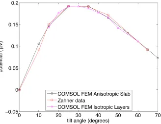
Using both the ILM and the ASM, Zahner, et al. [16] device dimensions were
built using the CAD software that was included with the basic COMSOL package.
The dimensions were 8mm, 6mm, 2mm for the length, width, and height respectively.
A constant heat flux density of 10(mW/cm2) was input across the top surface while
the angle of inclination of the layers was varied. The geometry of the experiment
can be seen in Fig. 3.3 [16]. As can be seen in the plot of the data obtained in
both models in Fig. 3.4 as well as the data in Zahner et al. [16], there is a close
agreement between experiment and simulation of the Seebeck effect for this device.
It was determined that each of the physics interfaces built were sufficiently accurate
to continue with a computational analysis of the Seebeck effect.
The paper by Kyarad and Lengfellner [6] was used as the basis in the validation
process for the Peltier effect. As stated in their paper, the experiment’s boundary
conditions were not kept constant. It is stated that, ”the sample bottom is heated
above the coolant temperature due to insufficient thermal coupling.” [6] Therefore,
without adding this heat flux into the simulation, a difference in computations and
measured data was expected. The experimental set up is pictured in Fig. 3.5 [6].
Figure 3.5: Experimental set up in Kyarad et al. [6] in which a current is injected into the left face, and Peltier cooling occurs across the top of the device with the bottom face kept at constant temperature.
In a paper by Ali, et al. [17] different heat fluxes were implemented to simulate the
qualitative aspects were seen in the simulations, the simulations were unsuccessful
in matching the measured data. The same parabolic qualitative aspects of the data
were seen in the COMSOL computations. COMSOL computations were measured
at the midpoint of the sample. A surface average was also computed across the
entire top surface where the cooling occurred. It turns out that the midpoint and
the surface average are quite close, and both computations are plotted along with
the Kyarad data in Fig. 3.6 [6]. As expected the discrepancy between the COMSOL
adiabatic boundary conditions and the measured data is apparent. The ILM did not
converge with the ASM as it did in computing the Seebeck effect. The difference
between the two models was investigated and is explained in section4.2.
3.3
Transverse Seebeck Effect
The transverse Seebeck effect occurs when a temperature difference is applied in
the z-direction a potential difference occurs in the x-direction as in Fig. 3.7. In order
to study the transverse Seebeck effect various boundary conditions and geometries
were built in the ILM and ASM. The geometry varied in aspect ratios for ∆x/∆z <1
and ∆x/∆z >1. The angle of inclination ranged from 0 to π/2.
Figure 3.7: Diagram of the transverse Seebeck effect simulation where a temperature difference is in z-direction, and the potential difference is calculated in the x-direction.
With a temperature difference applied in the z-direction, a transverse potential
current equation along with the open circuit condition gives us the electric field.
Ex=ρxxJx+ρxzJz−Sxx
∂T ∂x −Sxz
∂T
∂z =−∇xV (3.1)
Integrating along the x-direction will give the potential
VL−V0 =−
ˆ L
0
Exdx=−
ˆ L
0
ρxxJx+ρxzJz+Sxx
∂T ∂x +Sxz
∂T ∂z
dx (3.2)
VL−V0 =
ˆ L
0 Sxx
∂T ∂xdx+
ˆ L
0 Sxz
∂T ∂zdx−
ˆ L
0
(ρxxJx+ρxzJz). (3.3)
It mat be assumed that Jx and Jz are zero since there is an open circuit condition
applied to the device; however, eddy currents occur in the simulations. The effects
are smaller than the Seebeck thermopotential components of the sum but are not
negligible. The last integral in Eq. 3.3must be taken into account as it subtracts from
the thermopotential. However, a qualitative understanding of the thermopotential’s
dependence on aspect ratio can be achieved by looking at the first two terms in Eq.
3.3.
VL−V0 ≈
ˆ L
0 Sxx
∂T ∂xdx+
ˆ L
0 Sxz
∂T
∂zdx. (3.4)
This equation depends on the temperature gradient components in the x and z
directions, ∂T /∂x and ∂T /∂z respectively. These quantities take on a parabolic
nature, but for a qualitative understanding, they can be approximated with
∂T ∂z ≈
Th−Tc
d and
∂T ∂x ≈
TL−T0
whereTh and Tc are the constant applied boundary conditions in the z-direction. TL
is the temperature at x=L, andT0 is the temperature at x= 0. Substituting these
expressions into the integrals
VL−V0 ≈Sxx
TL−T0 L
ˆ L
0
dx+Sxz
Th−Tc
d
ˆ L
0
dx (3.6)
VL−V0 ≈Sxx(TL−T0) +Sxz(Th−Tc)
L d
. (3.7)
The dependence on the aspect ratio (L/d) is explicit in the approximation. A device
that is longer will produce a higher potential difference. It turns out that the
poten-tial adds in series along the transverse direction. A longer device will have a higher
potential, all other conditions unchanged, but there is a loss mechanism at play.
There is no current input through the device in this study, but eddy currents form
as shown in Eq. 2.56. As discussed below the eddy currents form to the detriment
3.4
Transverse Peltier Effect
The transverse Peltier effect occurs when a current is applied to a device in one
direction, and cooling occurs on one side of the device in a direction perpendicular
to the flow of current. Fig. 3.8 illustrates this configuration for current in the
x-direction and cooling in the z-x-direction. In this study the current was varied from
1 Amp to as high as 80 Amps in some simulations in order to find the maximum
amount of cooling that could occur.
Figure 3.8: Diagram of the transverse Peltier effect simulation where a current is injected in the z-direction, and heat flows in z-direction to cool off the top plate.
In the simulations the conditions for the y-component of heat flow are no current
in the y-direction Jy = 0 as well as no temperature difference ∂T /∂y = 0.
governing the heat flow in a transverse thermoelectric device are then
JxQ =JxSxxT +JzSxzT −κxx
∂T ∂x −κxz
∂T
∂z (3.8)
JzQ =JxSzxT +JzSzzT −κzx
∂T ∂x −κzz
∂T
∂z. (3.9)
Jz is not zero as we get an electric field component from 2.50 directing some
current in the z-direction.
Ez =Jxρzx+Jyρzy+Jzρzz−Szx
∂T ∂x −Szz
∂T
∂z (3.10)
So, bothJx and Jz contribute to the heat flux. Joule heating is accounted for in the
weak form equations input for the FEM solver in COMSOL. This opposes Peltier
Chapter 4
Results
4.1
Transverse Seebeck Effect
4.1.1
Aspect Ratio and Output Voltage
A simple analysis of the coupled current equations reveals how the output voltage
depends on the aspect ratio. This understanding is important in order to maximize
the thermopower for geometric constraints of a device needed in a specified circuit.
After confirming the validity of the models, the models were compared more
thor-oughly to determine if there was a point at which either broke down. Any differences
in the two models also needed to be known to account for any discrepancies in
Voltage Profiles
Examining the potential drops across a device given a certain temperature difference,
we see in Fig. 4.1 that the two models have a predictable difference. The ASM is
a mathematical idealization while the ILM has a discrete nature due to the layers’
interfaces throughout the model. As a consequence the ASM has smoother profiles
than does the ILM.
Figure 4.1: Difference in voltage drop profile across z-axis for the ASM and ILM in a Seebeck effect simulation.
4.1.2
Angle of Inclination and Aspect Ratio
was set in the z-direction and a potential difference calculated in the x-direction. The
bottom surface was kept at 273.15K while the top surface was held at 263.13K. The
aspect ratio ∆x/∆z was varied in the x-direction to determine what, if any, effect
this would have on the output transverse voltage. For each of the varying aspect
ratios, the of angle of inclination was varied to see if there is a relationship between
the two.
Figure 4.2: Seebeck effect model comparison of ILM and ASM for aspect ratios ∆x/∆z = (10,5,2, .5).
Fig. 4.2 implies that for the maximum output potential, there is a relationship
aspect ratio of ∆x/∆z = 10, the maximum output voltage migrates with changing
aspect ratio. For longer devices the maximum voltage is produced closer and closer
to an angle of 45◦. Since the relationship between the electric field produced depends
on the angle of inclination, we can find a function that maximizes both the potential
and the electric field from the coupled current equations. Simply set the derivative
equal to zero and then solve for the angle α.
Looking at the x component of the electric field equations and for the moment
neglecting the eddy currents
Ex=−Sxx
∂T ∂x −Sxz
∂T ∂z = ∂V ∂x (4.1) ∂Ex ∂α = ∂ ∂α Sxx ∂T ∂x +Sxz
∂T ∂z
= 0. (4.2)
Plugging in our expressions forSxx and Sxz after rotation, we have
∂Ex
∂α = ∂ ∂α
Skcos2(α) +S⊥sin(α)2 ∂T
∂x − Sk −S⊥ 1
2sin(2α)
∂T ∂z
= 0
(4.3)
−2Skcos(α)sin(α) + 2S⊥sin(α)cos(α) ∂T
∂x − Sk−S⊥
cos(2α)∂T
∂z = 0.
Now, simplifying
sin(2α) S⊥−Sk ∂T
∂x + S⊥−Sk
cos(2α)∂T
∂z = 0 (4.5)
sin(2α) S⊥−Sk ∂T
∂x =− S⊥−Sk
cos(2α)∂T
∂z (4.6)
tan(2α) =− ∂T ∂z ∂T ∂x (4.7)
α= 1
2arctan
−
Td−Tz=0 d
TL−Tx=0 L
(4.8)
α= 1
2arctan
−
Td−Tz=0 TL−Tx=0
L d
. (4.9)
S⊥−Sk
is never zero since S⊥ and Sk will always have different values. While
expression4.9is an approximation, the implicit dependence of the angle of inclination
α on the aspect ratio ∆x/∆z =L/d seen in the simulations is affirmed.
4.1.3
Seebeck Tensor and Potential
As pointed out, the off diagonal term of the rotated Seebeck tensor Sxz reaches
its maximum at 45◦. Naturally the question arises as to why this occurs. An
exam-ination of the Seebeck coefficients provides some mathematical insight into what is
happening. The Seebeck tensor components contributing in Eq. 4.1 are the Sxx and
Sxz are, respectively,
Sxx =Skcos2(α) +S⊥sin2(α) (4.10)
Sxz =
1
2 Sk −S⊥
Fig. 4.3 shows the components plotted for angles of inclination 0◦−90◦. It is clear
that for angles higher than 45◦theSxxcomponent has the higher magnitude. There is
an important aspect as to what is happening to the components during the rotation:
Sxx switches from Sk toS⊥. So for devices with an aspect ratio less than 1, a higher
angle of inclination will produce higher voltages.
Figure 4.3: Magnitude of Seebeck components,Sxz and Szz for angles of inclination
0◦-90◦.
The Seebeck components are scaled by the temperature gradients in the x and z
ASM gives the potential across the block.
V =
ˆ L
0 Sxx
∂T ∂xdx+
ˆ L
0 Sxz
∂T ∂zdx−
ˆ L
0
(ρxxJx+ρxzJz)dx. (4.12)
Figure 4.4: Magnitude of voltage components contributing to x component of the thermoelectric field for angles of inclination 0◦-90◦.
The integrals of the eddy current contributions, the Seebeck thermopotential
contributions, the total potential, and the FEM solution are shown in Fig. 4.4. It
was first assumed that Jx and Jz were zero since there was no current injected into
the device. The line integral of the Seebeck contributions computed overshoots the
and so, Jx and Jz are not equal to zero and must be considered in the integral. It
turns out that the eddy current contributions were precisely the difference needed to
correct for the aforementioned assumption.
4.1.4
Eddy Currents in the ASM and ILM
Eddy currents must be taken into account for accurate understanding and
mod-eling of the Seebeck effect in transverse thermoelectric devices. These currents take
on different distributions for the ILM and ASM. The reason, as stated in Anatychuk
and Luste [10], is due to the surface to surface interfaces in the ILM. Due to the jump
discontinuities at each interface of the Seebeck coefficients, a surface perpendicular
electric field component E⊥ will contribute to the direction of the currents. Some
similarities in the ILM and ASM are seen in the eddy current directions. The E⊥
redirects some of the eddy currents in the ILM as can be seen in Figs. 4.5, 4.6, 4.7,
Figure 4.5: ASM (left) and ILM (right) shown with normalized eddy current densities for open circuit Seebeck potential at 45 degree angle of inclination, aspect ratio of 1/2, and ten degree temperature difference top to bottom.
Figure 4.7: ASM normalized eddy current density for open circuit Seebeck potential at 45 degree angle of inclination, aspect ratio of 2/1, and ten degree temperature difference top to bottom.
4.1.5
Mathematical Difference in ILM and ASM
There is clearly a difference between eddy currents distributions in the ILM and
ASM. The difference occurs in the application of Eq. 2.56. An examination of the
eddy current equations with specific geometrical considerations from the transverse
thermoelectric device described in section 2.2.2 provide the mathematical footing
needed to understand thermoelectric eddy currents. Indicial notation comes in handy
in for compact notation.
∇ ×E=−∂B
∂t (4.13)
(∇ ×E)i =ijk∂jEk (4.14)
ijk∂jEk= 0 (4.15)
Using Eqs. 2.48-2.53 and substituting them in Eq. 4.15, and breaking the cross
product into components gives:
x component
(∇ ×E)x =xjk∂jEk (4.16)
(∇ ×E)x =∂yEz−∂zEy (4.17)
0 = ∂
∂y
ρzxJx+ρzzJz−Szx
∂T ∂x −Szz
∂T ∂z
− ∂
y component
(∇ ×E)y =yjk∂jEk (4.19)
(∇ ×E)y =∂zEx−∂xEz (4.20)
0 = ∂
∂z (ρxxJx+ρxzJz)− ∂ ∂z
Sxx
∂T ∂x +Sxz
∂T ∂z − ∂ ∂x
ρzxJx+ρzzJz−Szx
∂T ∂x −Szz
∂T ∂z
(4.21)
z component
(∇ ×E)z =zjk∂jEk (4.22)
(∇ ×E)z =∂xEy −∂yEx (4.23)
0 = ∂
∂x(ρyyJy)− ∂ ∂y
ρxxJx+ρxzJz −Sxx
∂T ∂x −Sxz
∂T ∂z
(4.24)
Equations 4.18, 4.21, and 4.24 describe eddy currents in an anisotropic material.
Jy 6= 0, but it is six orders of magnitude less than Jx and Jz as computed in the
models and can be neglected. There is no y dependence for any of the variables, so
the ˆx and ˆz components tell nothing about the system.
Eddy Currents in the ASM
The ASM is a pure mathematical model, and, hence, has certain idealistic
per-pendicular and parallel components that are continuous throughout the anisotropic
slab. Consequently, the material parameters are constants and are not spatially
dependent. Examining the ˆy component left from the curl of E
∂ ∂z
ρxxJx+ρxzJz−Sxx
∂T ∂x −Sxz
∂T ∂z = ∂ ∂x
ρzxJx+ρzzJz−Szx
∂T ∂x −Szz
∂T ∂z
(4.25)
Looking at the left hand side
∂ ∂z
ρxxJx+ρxzJz−Sxx
∂T ∂x −Sxz
∂T ∂z (4.26) ρxx ∂Jx
∂z +ρxz ∂Jz
∂z −Sxx ∂2T
∂z∂x −Sxz ∂2T
∂z2, (4.27)
and then the right hand side
∂ ∂x
ρzxJx+ρzzJz−Szx
∂T ∂x −Szz
∂T ∂z (4.28) ρzx ∂Jx
∂x +ρzz ∂Jz
∂x −Szx ∂2T
∂x2 −Szz ∂2T
∂x∂z. (4.29)
Now, ρxz = ρzx and Sxz = Szx. Bringing the pieces back together and simplifying
gives
ρxx
∂Jx
∂z +ρxz ∂Jz ∂z − ∂Jx ∂x
−ρzz
∂Jz
∂x
=Sxz
∂2T
∂z2 − ∂2T ∂x2
+Sxx
∂2T
∂z∂x −Szz ∂2T ∂x∂z.
Eddy Currents in the ILM
The situation gets more complicated in the ILM since the coefficients are spatially
dependent over each layer of alternating materials. The product rule must be used
for each term in the sums. Again looking at the y component. The left hand side
says
∂ ∂z
ρxxJx+ρxzJz−Sxx
∂T ∂x −Sxz
∂T ∂z
(4.31)
∂ρxx
∂z Jx+ρxx ∂Jx
∂z + ∂ρxz
∂z Jz+ρxz ∂Jz
∂z
− ∂Sxx ∂z
∂T
∂x −Sxx ∂2T ∂z∂x −
∂Sxz
∂z ∂T ∂z −Sxz
∂2T ∂z2,
(4.32)
and then the right hand side
∂ ∂x
ρzxJx+ρzzJz−Szx
∂T ∂x −Szz
∂T ∂z
(4.33)
∂ρzx
∂x Jx+ρzx ∂Jx
∂x + ∂ρzz
∂x Jz+ρzz ∂Jz
∂x
− ∂Szx ∂x
∂T
∂x −Szx ∂2T ∂x2 −
∂Szz
∂x ∂T ∂z −Szz
∂2T ∂x∂z.
Then again putting the pieces back together
ρxx
∂Jx
∂z +ρxz ∂Jz ∂z − ∂Jx ∂x
−ρzz
∂Jz ∂x + ∂ρxx ∂z − ∂ρzx ∂x
Jx+
∂ρxz ∂z − ∂ρzz ∂x Jz
=Sxz
∂2T
∂z2 − ∂2T
∂x2
+Sxx
∂2T
∂z∂x −Szz ∂2T ∂x∂z − ∂Szx ∂x − ∂Sxx ∂z ∂T ∂x − ∂Szz ∂x − ∂Sxz ∂z ∂T ∂z (4.35)
The situation becomes more complicated in the ILM as seen by comparing Eq.
4.30 and Eq. 4.35. There are 8 more terms in (∇ ×E)y equation in the ILM than
the ASM. The results are seen by the more complicated current density directions
in the ILM in Figs. 4.5, 4.6, 4.7, and 4.8.
Effect of Width
In the description of transverse thermoelectric effects in the previous chapter only
two dimensions were discussed. The reason is that the third dimension is of no
consequence, but this statement definitely needs to be qualified. So simulations were
run with a varying third dimension to demonstrate that there is no variation in the
Figure 4.9: Effect of width on the ASM for angles of inclination 0◦-90◦.
The Seebeck study provided some interesting results. Eddy currents occur and
must be taken into account when running simulations to compute thermopower.
The dimension of the device determine which angle of inclination should be used for
maximum thermopower output. The thermoelectric effect is a thermodynamically
reversible process, and the computational study of the Peltier effect is presented
4.2
Transverse Peltier Effect
In this study an electrical current boundary condition was input to model the
Peltier effect. The angle of inclination was kept at 25◦, and the bottom surface was
held at 295K as in the Kyarad experiment. Different current densities were input
for different aspect ratios. Both models have a temperature gradient along the top
of the device where the cooling occurs. The temperature was taken in the middle of
the top surface as this location was shown to be in close agreement with the surface
average. Bismuth telluride and lead were the materials used for the study. The
materials’ parameters used are the same as found in Table 1 in Kyarad [6] with the
exception that a Seebeck coefficient of 200(µV /K) was used instead of 20(µV /K).
4.2.1
Peltier Aspect Ratio Comparison
While in the Seebeck study the ASM and ILM agreed extremely well over
dif-ferent geometries and conditions, the Peltier simulations diverged for certain device
geometries. In the Peltier studies Fig. 4.11, the ILM diverged significantly at lower
aspect ratios with the layer thickness of 1mm used in the Kyarad experiment [6]. This
includes the aspect ratio used in [6]. At the aspect ratio of 5 the models converge,
and the results for longer aspect ratios are discussed next.
In Fig. 4.12 the ILM shows a small decrease in ∆T for aspect ratio ∆x/∆z = 10.
This implies an engineering limit in geometry for Peltier coolers as for longer devices
Joule heating will start to overtake the Peltier cooling. Keeping the cross sectional
area the same as in done in the studies, this makes sense looking at the equation for
Joule heating
Q∝I2R = I2ρ
L A
. (4.36)
Peltier Model Convergence: Layer Thickness
The ILM converges to the ASM when the layer thickness was reduced as shown in
Fig. 4.13. This is a comforting result in the limit, however it may be a drawback of
the ILM in general as it diverges significantly from measured data.
4.2.2
ASM and ILM Differences
Temperature Distribution
As noted for the potential in the Seebeck studies, there is a similar difference in
distribution of temperature in the Peltier studies. Again the ILM has a digital effect
from the inhomogeneity of the alternating material properties of each layer. In the
ILM the temperature is constant across most of each layer, and temperature drops
only occur at the interfaces of the two materials. This is a comforting result since
the Peltier is known to occur at material interfaces. The strict mathematical model
employed in the ASM has the smooth profile shown in Fig. 4.14. As noted in the
previous section, the temperature difference ∆T is greater in the ASM. This is an
important difference of the ILM. More comparisons to measured data are needed to
Figure 4.14: Difference in temperature distribution across x-direction for the ASM and ILM in a Peltier effect simulation.
Current Density Differences
A current density plot Fig. 4.15 show an important difference in the two
compu-tational models. There is a component in the ILM that does not show up in the
ASM. An input current in the x-direction mandates that a z directed electric field
component is generated as indicated in Eq. 4.37.
Ez =Jxρzx+Jzρzz−Szx
∂T
∂x
−Szz
∂T
∂z
(4.37)
Indeed the z component of the current density is seen in Fig. 4.15 is seen in both
be accounted for in the engineering of thermoelectric devices.
Figure 4.15: Current density plots for ILM and ASM showing the extra component in the ILM.
Zooming in for a closer look at Fig. 4.16 and Fig. 4.17 reveals a component
perpendicular to the contact surfaces in the ILM not seen in the ASM. This J⊥ at
a surface interface is directed by an E⊥ as described in the paper by Anatychuk
and Luste [10]. E⊥ occurs throughout the model in all the Peltier effect simulations
using the ILM.E⊥ only occurs in ”zonally inhomogeneous structures” [10] with the
materials posessing different Seebeck coefficients. Moreover Anatychuk and Luste
state that theE⊥fields lie along isotherms within the material. Utilizing the plotting
capabilities in COMSOL, it looks as though they are correct as there are isothermal
surfaces that intersect the contact surfaces perpendicularly. Ez is positive as seen
in both the ASM and ILM, however the z component of E⊥ is in the negative z
cooling.
Figure 4.16: Zoomed in current density plot for the Peltier ILM simulation showing extra surface perpendicular component.
4.3
Device Engineering
4.3.1
ILM
Pictured below in Fig. 4.18 is a device with dimensions of 5cm x 5mm x 5mm.
The top and bottom plates are beryllium oxide, and the left and right plates are
copper. The materials in the middle alternate between lead and p-type bismuth
telluride.
Figure 4.18: Single transverse thermoelectric device geometry built in the ILM.
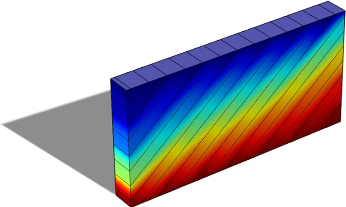
Fig. 4.19shows the potential distribution over a transverse thermoelectric device
with heat flux applied of 137,000(W/m2) to top, and 0V held at right side. The
choice of 137,000(W/m2) for the input heat flux simulates a magnification of 100
times that of sunlight which has a heat flux of 1370(W/m2). The bottom surface is
the heat sink.
Figure 4.19: ILM surface plot of the potential distribution over a transverse ther-moelectric device with heat flux applied of 137,000(W/m2) to top, and 0V held at
right side.
4.3.2
ASM
The ILM geometries are more realistic than the ASM, so the ILM CAD device
geometries are more complicated. Consequently, creating devices for the ILM takes
much longer than creating devices in the ASM. It is possible to create geometries
in other CAD programs and import them into COMSOL which could simplify the
process of creating complicated geometries in the ILM. Although the ASM is an
idealization, building a model a large set up for a device takes much less time. The
ASM Fig. 4.20plots the potential across the mathematical model of the ILM device
Figure 4.20: ASM model of a single transverse thermoelectric with heat flux applied of 137,000(W/m2) to the top section, and 0V held at bottom right side copper plate.
Fig. 4.21pictures an array of single devices electrically linked in series with copper
plates. Each leg is made of the same two types of materials, so unlike longitudinal
thermoelectric devices, only one type of thermoelectric semiconductor is needed to
build a device. The important aspect that needs to be considered is the orientation
of each thermoelectric leg. Each leg must be oriented 180◦ relative to the next. This
is must be the case if the voltages are to add in series rather than simply cancel each
other out. This being the case, the potentials add in series. The potential is higher in
the ASM Fig. 4.20 than in the ILM Fig. 4.19, and these differences need to be more
thoroughly examined. Regardless of the differences, the ASM can be used to get an
upper bound on device output. The ASM physics module needs to be generalized
somewhat in order to achieve an effective simulation. The more robust ASM will be
modeled in more complicated devices.
Figure 4.21: Transverse thermoelectric device linked in series with heat flux applied of 137,000(W/m2) to the top of each section, and 0V held at bottom right side copper plate.
This section provides the evidence that transverse thermoelectric devices can
be modeled and engineered in a computational environment in COMSOL. Further
device geometries and environmental conditions can be input in order to compare
outputs before spending the time and money creating physical devices and taking
measurements.
The transverse Seebeck and Peltier effects have been shown to be effective. Open
circuit eddy currents and surface interface electric fields have proven to be interesting
effects that must be taken into account to understand transverse thermoelectrics.
More studies are needed to determine the necessary materials and conditions needed
Chapter 5
Conclusion
COMSOL Multiphysics uses the finite element method (FEM) to compute numerical
solutions and was the main software used in the analysis of the transverse
thermo-electric effect done for this thesis. As COMSOL does not have a thermothermo-electric
module, two COMSOL physics modules were built for modeling and research. The
purely mathematical model named the anisotropic slab model (ASM) provides the
ideal case with which to compare the isotropic layer model (ILM). The ILM provides
the more realistic model as the geometries and boundary conditions match what
an actual device will encounter. The differences in ILM FEM solutions are noted
throughout the thesis and provide computational evidence as to predicted effects
such as anisotropic eddy currents and surface to surface interface effects. Validation
with measured data along with the computational evidence for the aforementioned
effects prove the reliability of the custom physics modules.
Noted also was that although no current was injected into the device, eddy currents
are generated and have a significant effect on the output potential that cannot be
neglected. The angular dependence on output was shown to originate from the
competition of the longitudinal Seebeck element Sxx and the off diagonal element
Sxz of the Seebeck tensor. The third dimension has no effect on the output and,
hence, does not need to be considered for loss mechanisms. Transverse Seebeck
effect is shown to be a reliable mechanism for thermoelectric device engineering.
The transverse Peltier effect was shown to have a cooling effect of approximately
20K. In the ILM portions of the current were directed perpendicularly to the layers’
interfaces through out the device. This perpendicular component was absent in
the ASM since it is an idealization without layer to layer interfaces. As seen in the
simulations, when the layer thickness is reduced the ILM converges to the ASM. This
is a deficiency in the ILM since certain device geometries might have comparable layer
thickness relative to the dimensions of the device. Temperature drops in the ILM
were shown to occur at the interface of the layers while the ASM was shown to have
a continuous drop. The transverse Peltier effect exhibits possibilities for applications
such as computer chip cooling.
Transverse thermoelectric devices have promising future in energy conversion and
heat transfer. At a cost of approximately $10,000 per pound to carry a load into
space, reduction in material to power spacecrafts opens up a valuable margin which
can be utilized for more computational power or simply less cost. In any process
which produces heat loss, transverse thermoelectric devices could be could be used
conversion is yet another application that should drive research and development

![Figure 3.3: Experimental set up in Zahner et al. [16] with constant heat flux appliedto sample top, the bottom face held at constant temperature, and potential differencecalculated from left to right.](https://thumb-us.123doks.com/thumbv2/123dok_us/8926289.1845497/40.612.140.465.305.571/figure-experimental-constant-appliedto-constant-temperature-potential-dierencecalculated.webp)
![Figure 3.5: Experimental set up in Kyarad et al. [6] in which a current is injectedinto the left face, and Peltier cooling occurs across the top of the device with thebottom face kept at constant temperature.](https://thumb-us.123doks.com/thumbv2/123dok_us/8926289.1845497/42.612.153.460.260.490/figure-experimental-injectedinto-peltier-cooling-thebottom-constant-temperature.webp)