Volume 3, Issue 2, 2016
12
Available online at www.ijiere.com
International Journal of Innovative and Emerging
Research in Engineering
e-ISSN: 2394 - 3343 p-ISSN: 2394 - 5494
PCIe CHECKER LIBRARY
GENERATION OF SEQUENCES & DRIVER COMPONENT FOR
EP LTSSM USING UVM
Vijayashree.Ganesh.Pyati
KLE Institute Of Technology, Hubli, Karnataka, India
ABSTRACT:
Verification of complex systems like PCIe in SystemVerilog is a complicated process for a verification engineer, but if we adopt a standard methodology like UVM we can reduce time to verify and hence increase the efficiency. One can exploit object oriented programming to the core in UVM rather than using SystemVerilog. The objective of the project is to construct a PCIe checker library which verifies LTSSM of PCIe i.e passive monitor which can be hooked on a PCIe interface connecting different PCIe devices. The devices can be upstream or downstream. In this project we are creating a Bus functional model(BFM) PCIe endpoint, which drives PCIe packet to the serial interface, creating a stimulus library. This provides meaningful transaction which consists of different ordered sets (control information) to the BFM model for establishing the link between the two PCIe devices. This information is continuously monitored by the passive monitor. All test cases are subjected to verification of the functionality of passive monitor and coverage report is generated. This checkers Library will be compatible with version 1.0, 2.0, 3.0 of PCIe Specification and has been implemented in UVM.
Keywords— PCIe, LTSSM, passive monitor, BFM, endpoint, UVM.
I. INTRODUCTION
PCI Express (Peripheral Component Interconnect Express), officially abbreviated as PCIe, is a high-speed serial computer expansion bus standard designed to replace the PCI, PCI-X, and AGP bus standards. PCIe has numerous improvements over the older standards, including higher maximum system bus throughput, lower I/O pin count and smaller physical footprint, better performance scaling for bus devices, a more detailed error detection, reporting mechanism (Advanced Error Reporting, AER), and native hot-plug functionality. PCI Express link represents a dual-simplex communications channel between two components. The fundamental PCI Express link consists of two, low-voltage, differentially driven signal pairs: a transmit pair and a receive pair. The primary link attributes are link, lane, signaling rate, initialization. There are three discrete logical layers: the transaction layer, the data link layer, and the physical layer. Each of these layers is divided into two sections: one that processes outbound (to be transmitted) information and one that processes inbound (received) information [5].The different layers of PCIe is shown in figure 1.1.
Volume 3, Issue 2, 2016
13 Figure. 1. 1. PCIe layers [5].
II. PCIE 3.0 LTSSM
Link Training and Status State Machine defines the set of rules for root complex, end point and switch devices. The LTSSM has been characterized in five different categories as follows:
Link training states Link re-training states Power management states Active power management states Other states
Figure. 2. 1. Link training status and state machine [3]. The state and sub-states of link training status state machine is shown in figure 2.1.
A. DETECT STATE
Volume 3, Issue 2, 2016
14 Figure. 2. 2. Detect sub-states [3].
B. POLLING STATE
In the polling state, port transmits training ordered sets and responds to the received training ordered sets. The bit lock and symbol lock are established and lane polarity is configured[3]. The sub states of polling are shown in figure 2.3.
Figure. 2. 3. Polling sub-states [3].
C. CONFIGURATION STATE
In the configuration state, both the transmitter and receiver are sending and receiving data at the negotiated data rate. The lanes of a port configure into a link through a width and lane negotiation sequence[3]. The sub states of configuration are shown in figure 2.4.
Volume 3, Issue 2, 2016
15
D. L0 STATE
In the L0 state has normal operation where data and control packets can be transmitted and received. All power management states are entered from this state[3].
E. RECOVERY STATE
In the recovery state, both the transmitter and receiver are sending and receiving data using the configured link and lane number as well as the previously supported data rate(s). Recovery allows a configured link to change the speed of operation[3]. The sub states of recovery are shown in figure 2.5.
Figure. 2. 5. Recovery sub-states [3].
F. L0s STATE
L0s is intended as a power savings state.L0s allows a link to quickly enter and recover from a power conservation state without going through recovery. Transmitter and receiver lane pair on a port are not required to both be in L0s simultaneously [3]. The sub states of L0s transmitter and receiver are shown in figure 2.6 and figure 2.7 respectively.
Figure. 2. 6. L0s transmitter sub-states [3].
Volume 3, Issue 2, 2016
16
G. L1 STATE
L1 is intended as a power savings state. The L1 state allows an additional power savings over L0s at the cost of additional resume latency. The entry to L1 occurs after being directed by the Data Link Layer[3]. The sub states of L1 are shown in figure 2.8.
Figure. 2. 8. L1 sub-states [3].
H. L2 STATE
In the L2 state, power can be aggressively conserved. Most of the transmitter and receiver may be shutoff. Main power and clocks are not available, but auxiliary power is available. When beacon support is required by the associated system or form factor specification, an upstream port that supports the wakeup capability must be able to send; and a downstream port must be able to receive; a wakeup signal referred to as a beacon. The entry to L2 occurs after being directed by the Data Link Layer [3]. The sub states of L2 are shown in figure 2.9.
Figure. 2. 9. L2 sub-states [3].
I. DISABLED STATE
In the disabled state, the configured link is disabled until directed or electrical idle is exited (i.e., due to a hot removal and insertion) after entering disabled [3].
J. LOOPBACK STATE
In the loopback state, test and fault isolation is performed. Only the entry and exit behavior is specified, all other details are implementation specific. Loopback can operate on either per lane or configured link basis. A loopback master is the component requesting loopback. A loopback slave is the component looping back the data [3]. The sub states of L2 are shown in figure 2.10.
Volume 3, Issue 2, 2016
17
K. HOTRESET STATE
In the hot reset state,the system is reset and entered to this state if directed by a higher layer and ordered sets[3].
III. VERIFICATION
The verification of above LTSSM design for downstream port i.e endpoint device is carried out to check the coverage of states and substates. The link training and link re-training states has been monitored by creating test cases and sequences. Verification is done using UVM.
Figure. 3. 1. UVM test bench architecture[6].
A. TOP
Top level module has a clock generation block, instance of the interface. It also imports the PCIe_package and uvm_package.
Clock generation block selects the different clock speeds depending on the generation of the device, the default value is 2.5 GT/s. The frequency of which is changed in recovery speed state. The instance of Interface is passed to UVM_test_top environment by using the config_db.The test is started in the top level module by using run_test().The PCIe_package has all the user defined variable for change of state change, constant parameters and different ordered sets.
B. UVM_TEST_TOP
UVM_test_top consists of a base class which constructs the environment in the build phase and runs the different sequences on the sequencer. This is the place where the execution starts in the simulation phase by passing the handler of the sequence to sequencer. It has collection of different tests which passes different sequences to the sequencer. It get the virtual interface from the config_db and adds the configuration information and passes down to all the lower level components.
C. ENVIRONMENT
It is extended from uvm_env base class. It consists of handlers to the configuration item, agents, coverage collector. It gets the configuration items form config_db and passes to the agent. During build phase it builds the agents and the coverage monitor for RC and EP. The analysis ports of the agents are connected to analysis exports of the coverage_collector.
D. AGENT
Volume 3, Issue 2, 2016
18
E. RC SEQUENCER & EP SEQUENCER
Both the sequencer generates a sequence which consists of different ordered sets according to different LTSSM states. Both sequencer classes are derived from uvm_sequencer class. The transaction is transmitted to driver using start_item() and finish_item().
F. RC DRIVER & EP DRIVER
The ordered sets which are generated in sequencer are driven serially at the output by the both drivers. Both driver are derived from uvm_driver. These get transaction from RC sequencer and EP sequencer using seq_item_port. get_next_item() and seq_item_port.item_done().
G. RC MONITOR & EP MONITOR
Both the monitors are divided into two level of hierarchy namely bus monitor and LTSSM monitor with different functionalities. In the build phase the interface is obtained from the config_db, the TLM ports built which are used for communication among the monitors and communicating to the sequencer for change of state. The interface consists of RX, TX pins, d_clk and reset signals. Bus monitor are directly connected to the RX and TX bus which reads the differential signaling and decodes the data values and sends to the LTSSM monitor. LTSSM monitor does all the logical operations by taking the information from the bus monitor and updates the different states and also gives back the information to the bus monitor about when to go to idle state and when to obtain the symbol lock and read the data from the bus. It gives the information to the sequencer to change the sequences. It send the information to coverage collector to trigger different bins based on the states and state transitions condition covered.
H. COVERAGE COLLECTOR
Coverage collector is extended from uvm_subscriber. It consists of coverpoints for state covered, state transition conditions. The cross coverage information between state covered and state transition conditions gives all the information about all the conditions.
IV. TESTCASES
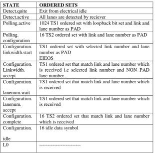
For the end point (downstream) device using different ordered tests i.e TS1, TS2, EIOS, EIEOS, SKIP 36 testcases and 12 sequences are generated. Table 1 explains the different ordered sets which are generated in particular states and sub-states.
TABLE 1. Ordered sets generated in all LTSSM states
STATE ORDERED SETS
Detect.quite Exit from electrical idle
Detect.active All lanes are detected by reciever
Polling.active 1024 TS1 ordered set with loopback bit set and link and lane number as PAD
Polling. configuration
16 TS2 ordered set with link and lane number as PAD
Configuration. linkwidth.start
TS1 ordered set with selected link number and lane number as PAD
EIEOS Configuration.
Linkwidth. accept
TS1 ordered set that match link and lane number which is received i.e selected link number and NON_PAD lane number..
Configuration. lanenum.wait
TS1 ordered set that match link and lane number which is received
Configuration. lanenum. accept
TS1 ordered set that match link and lane number which is received
Configuration. complete
16 TS2 ordered set that match link and lane number which is received
Configuration. idle
16 idle data symbol
Volume 3, Issue 2, 2016
19 Recovery.
rcvrlock
TS1 or TS2 ordered set with speed change bit 0 or 1 or TS1 or TS2 with speed change bit 1 and current speed is greater than 2.5GT/s or advertised data rate is greater than 2.5GT/s.
Electrical idle exit ordered sets(EIEOS)
TS1 or TS2 ordered set and speed not changed to new speed or speed changed to new speed.
Recovery. rcvrcfg
32 TS2 Ordered set and supported data rates are greater than 2.5 GT/s or current speed is greater than 2.5 GT/s. 16 TS2 with same link and lane number with identical data rate identifier and speed change bit as 0 or current data rate is 2.5GT/s or not higher data rate than 2.5GT/s Electrical idle exit ordered sets(EIEOS)
Recovery. speed
all lanes exit from electrical idle and speed changed to greater than 2.5GT/s or changed to speed when entered recovery state or changed to 2.5GT/s
Recovery. idle 16 idle data symbol
Skip ordered sets are transmitted at an average interval between 1180 to 1538 symbol timesin all states.
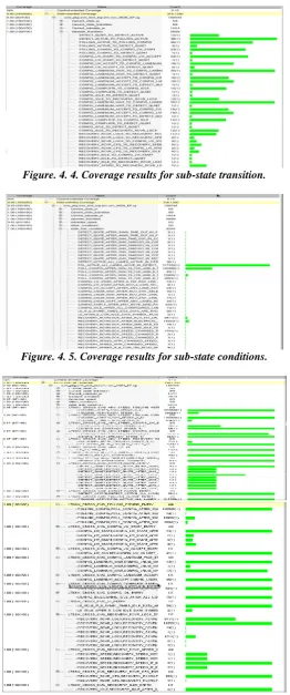
V. RESULTS
All the states of LTSSM are covered using sequences and test cases generated. Coverage of LTSSM state, state transition, sub-states, sub-states transition, sub-state conditions is obtained. All possible speeds i.e. 2.5GT/s and 5GT/s are obtained. Link width of X1, X2, X4, X8, X16, X32 are covered.
Figure. 4. 1. Coverage results for state covered and states transition.
Figure. 4. 2. Coverage results for sub-states.
Volume 3, Issue 2, 2016
20 Figure. 4. 4. Coverage results for sub-state transition.
Figure. 4. 5. Coverage results for sub-state conditions.
Volume 3, Issue 2, 2016
21
VI. CONCLUSIONS
Generation of sequences and driver component for end point device is successfully built and each and every test cases are covered for link training and link retraining process. Each and every states are entered at least once hence all states are covered. The speed 2.5GT/s and 5 GT/s is obtained. Fig 4.6 shows cross coverage of all states with the conditions is successfully obtained. The overall coverage obtained is 93%. For end point device the condition covered are 159 out of 165 as verification for 8 GT/s conditions are not performed. Hence this implementation can be extended for 8 GT/s.
REFERENCES [1] “PCI Express Base Specification,” Revision 1.0, April 29, 2002. [2] PCI Express 2.0 Base Specification,” Revision 0.9, September 11, 2006 [3] PCI Express Base Specification,” Revision 3.0, November 10, 2010.
[4] Rohit Kumar, Hardik Trivedi, Nitish Alok, “Design and Verification of USB 3.0 Link Layer(LTSSM).” International Journal of Computer Science and Information Technologies, Vol. 5 (4) , 2014.
[5] Ravi Budruk, Don Anderson & Tom Sanely,“ PCI Express System Architecture” , Mindshare Inc., 2003,pp 397-451.
![Figure. 1. 1. PCIe layers [5].](https://thumb-us.123doks.com/thumbv2/123dok_us/8874613.1816107/2.595.223.378.66.261/figure-pcie-layers.webp)
![Figure. 2. 2. Detect sub-states [3].](https://thumb-us.123doks.com/thumbv2/123dok_us/8874613.1816107/3.595.208.425.480.710/figure-detect-sub-states.webp)
![Figure. 2. 5. Recovery sub-states [3].](https://thumb-us.123doks.com/thumbv2/123dok_us/8874613.1816107/4.595.164.426.179.424/figure-recovery-sub-states.webp)
![Figure. 2. 9. L2 sub-states [3].](https://thumb-us.123doks.com/thumbv2/123dok_us/8874613.1816107/5.595.256.354.589.734/figure-l-sub-states.webp)
![Figure. 3. 1. UVM test bench architecture[6].](https://thumb-us.123doks.com/thumbv2/123dok_us/8874613.1816107/6.595.124.471.182.396/figure-uvm-test-bench-architecture.webp)