78
Improve Performance Static Random Access Memory Based on Design PLPSRAM
Lalit Gupta
1, Prof. Sumit Gupta
2Electronics and Communication Engineering, Department Oriental College of Technology, Bhopal, India 1[email protected], 2[email protected]
ABSTRACT: - In this field research paper explores the design and analysis of Static Random Access memories (SRAM) that focuses on optimizing delay and power. CMOS SRAM cell consumes very less power and have less read and write time. Higher cell ratios will decrease the read and write time and improve stability. PMOS semiconductor unit with fewer dimensions reduces the ability consumption. Our propose design propose low power static access memory (PLPSRAM) cell is implemented with reduced power and performance is good according read and write time, delay and power consumption. It’s been noticed typically that increased memory capability will increase the bit-line parasitic capacitance that successively slows down voltage sensing, to avoid this drawback use optimized scaling techniques and more, get improve performance of the design. Memories are a core a part of most of the electronic systems. Performance in terms of speed and power dissipation is that the major areas of concern in today’s memory technology. PLPSRAM cells supported 6T; 10T configurations are compared on the basis of performance for read and write operations. during this paper completely different static random access memory are designed so as to satisfy low power, high performance circuit of our propose design circuit PLPSRAM..
Keywords: - Static Random Access memories, Delay,
Power, six transistors, Write, Read, CMOS, PMOS.
I.
I
NTRODUCTIONRandom-access memory (RAM) is a form of pc data storage that stores frequently used program instructions to extend the final speed of a system. A random-access device permits knowledge things to be read or written in nearly the same quantity of your time irrespective of the physical location of information within the memory. In contrast, with different direct-access data storage media comparable to hard disks, CD-RWs, DVD-RWs and also the older drum memory, the time needed to read and write knowledge things varies considerably depending on their physical locations on the recording medium, because of mechanical limitations such as media rotation speeds and arm movement Static Random Access memories (SRAM) is scan/write memory devices which will read data from or write data to any of its memory addresses. The requirement for low power integrated circuits is well known due to their extensive use within the electronic portable equipments. On chip SRAMs
(Static Random Access Memory) confirm the power dissipation of SoCs (System on Chips) additionally to its speed of operation. Therefore it is important to own energy economical SRAMs. The use of SRAM is expected to extend in future for each portable and high performance micro chip. SRAM plays a crucial role in modern micro chip system, portable devices like pda, cellular phones, and transportable multimedia system devices. To achieve higher speed micro chip, SRAM primarily based cache memories are ordinarily used. The trend of scaling of device brings many challenges like power dissipation, sub threshold run, reverse diode run, and stability [1]. These days analysis on terribly low threshold voltage and ultra-thin gate chemical compound are in progressive stage, thanks to reduction within the threshold voltage and also the gate oxide thickness. The phenomena like intrinsic parameter fluctuation, random dopant fluctuation, oxides thickness fluctuation, and line edge roughness more degrade the stability of SRAM cells. Giant scale integration and fabrication process has resulted in increased density of devices by decreasing the device physical dimensions. Performance in terms of low power dissipation and high speed operation are the most important challenges of computer circuit style in deep submicron and nanoscale technologies. Designing high performance VLSI chip is becoming necessity for mobile communication and computing devices. Advances in battery technology haven't taken place as quick as advances within the electronic devices and systems. So, designing electronic systems having high performance in terms of high speed and low power dissipation may be a difficult task [2].
1.1 Types of Ram
79 it's the predominant type of memory device utilized in modern computers. Dynamic RAM is thought of volatile, because it lost |the information or data once power is off from the system [3].
1.2 Design of SRAM
A typical SRAM cell is created from six MOSFETs. Every bit in an SRAM is hold on four transistors (M1, M2, M3, and M4) that kind two cross-coupled inverters. This secondary cell has 2 stable states that are wont to denote zero and one. Two extra access transistors serve to manage the access to a secondary cell throughout read and write operations. Additionally to such six-transistor (6T) SRAM, different kinds of SRAM chips use four, 8, 10 (4T, 8T, 10T SRAM), or a lot of transistors per bit. Four-transistor SRAM is sort of common in complete SRAM devices (as critical SRAM used for CPU caches), implemented in special processes with an additional layer of polysilicon, allowing for very high-resistance pull-up resistors. The principal disadvantage of using 4T SRAM is increased static power because of the constant current flow through one in all the pull-down transistors. Access to the cell is enabled by the word line that controls the two access transistors M5 and M6 that, in turn, control whether or not the cell ought to be connected to the bit lines: BL and complementary BL. they're wont to transfer data for each scan and write operations. Though it's not strictly necessary to possess two bit lines, each the signal and its inverse are usually provided so as to enhance noise margins. Throughout read accesses, the bit lines are actively driven high and low by the inverters within the SRAM cell. The symmetric structure of SRAMs additionally permits for differential signaling, which makes little voltage swings a lot of simply detectable [4].
Fig1: Design approach of SRAM
1.3 SRAM Memory Cell Operation
AN SRAM cell has three completely different states.
Standby: - If the word line isn't declared, the access transistors M5 and M6 disconnect the cell from the bit lines. The 2 cross-coupled inverters shaped by M1 – M4
can still reinforce one another as long as they're connected to the supply [5].Reading:- In theory, reading only needs asserting the word line WL and reading the SRAM cell state by one access semiconductor and bit line, e.g. M6, BL. however, bit lines are comparatively long and have massive parasitic capacitance. to speed up reading, a additional advanced method is used in practice: The browse cycle is started by precharging each bit lines BL and BL, i.e., driving the bit lines to a threshold voltage (midrange voltage between logical one and 0) by an external module (not shown within the figures). Then asserting the word line WL permits each the access transistors M5 and M6, that causes the bit line BL voltage to either slightly drop m3 is ON and high PMOS transistor M4 is off) or rise (top PMOS transistor M4 is on). It ought to be noted that if BL voltage rises, the BL voltage drops, and vice versa. Then the BL and BL lines can have little voltage distinction between them. Ways amplifier can sense that line has the upper voltage and therefore verify whether or not there was 1 or 0 stored [6]. Writing:- The write cycle begins by applying the value to be written to the bit lines. If we tend to would like to put in writing a zero, we'd apply a zero to the bit lines, i.e. setting BL to one and BL to zero. This is often like applying a reset pulse to an SR-latch that causes the flip flop to alter state. A one is written by inverting the values of the bit lines. WL is then declared and therefore the value that's to be kept is secured in. This works as a result of the bit line input-drivers are designed to be much stronger than the relatively weak transistors within the cell itself so that they will simply override the previous state of the cross-coupled inverters. In follow, access NMOS transistors M5 and M6 have to be compelled to be stronger than either bottom NMOS (M1, M3) or high PMOS (M2, M4) transistors. This is often simply obtained as PMOS transistors are much weaker than NMOS once same sized. Consequently once one semiconductor combine (e.g. m3 and M4) is only slightly overridden by the write method, the other transistors combine (M1 and M2) gate voltage is additionally modified. This means that the M1 and M2transistors are often easier overridden, and so on. Thus, cross-coupled inverters amplify the writing method [7-8].
II. LITERATURE SURVEY
80 discharging bitbar line. Thus, a differential voltage develops between the BL and BL. This small potential difference between the bit lines is sensed and amplified by the sense amplifiers at the data output.
Fig 2: Design 6T SRAM
Shilpi Birla1 et al. [10]. Analyzed 8T Static Random Access Memory cell at 65nm process technology is shown in fig.3 This topology was originally proposed for a subthershold static RAM design and optimized for functionality and performance over a large voltage rang. A write operation is performed through WWL, WBL and WBLX port, where as single ended read operation is exercised through RWL and RBL ports.RBL is precharged at the end of each read cycle and keeps precharged during a write cycle.
Fig3: 8T SRAM cell
In this bit cell write and read ports are decoupled in contrast to the traditional 6T cell. Read-SNM problem is eliminated and 6T static RAM part can be sized for better writeablity without trading off RSNM. This makes the voltage drop across unaccessed read buffers zero and hence leakage on read bit line is highly reduced. Vdd is the virtual supply nodes for the cross coupled inverters and its voltage can be brought down during a write access to weaken PMOS load device and easewriteability problem at low voltage. Since the entire bit cells on a row are written and read at the same time, Vdd is shared across one row of memory cells.
Kursun V. et al. [11]. Introduce 9T SRAM is shown in Fig.4 Write occurs just as in the 6T SRAM cell. Reading occurs separately through N5, N6 and N7 controlled by the read signal (RWL) going high. This design has the problem of the high bit line capacitance with more pass transistors on the bit line.
Fig 4: 9T SRAM Cell
Arora N et al. [12]. proposes the fully differential low power 10T SRAM [10] bit cell is shown in Fig.5. The design strategy of cell is the series connection of tail transistor. The gate electrode of this device is controlled by the output of an XOR gate, inputs of which are tapped from write word line (WWL) and read word line (RWL) control signals coming from the WWL and the RWL drivers. The XOR gate and the tail transistor are shared by all the cells in a row. The tail transistor has to be appropriately up sized for sinking currents from all the cells in the row. Without this read buffer, a cell with such small drivers and series connected tail transistor would exhibit unacceptably low read static noise margin (RSNM), resulting in read instability.
81
III.
PROBLEM
FORMULATION
The main purpose of this paper is to reduce power dissipation during the Write operation in CMOS SRAM cell. Other factor like- cell area, switching delay, power dissipation and how many transistors are used in the implementation of SRAM are also optimizing.
IV. SIMULATION & RESULT ANALYSIS
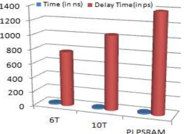
Micro-wind tool is truly integrated Electronic design automation software encompassing IC designs from concept to completion, enabling chip designers to design beyond their imagination. Microwinds integrate traditionally separated front-end and back-end chip design into an integrated flow, accelerating the design cycle and reduce design complexities. It tightly integrates mixed-signal implementation with digital implementation, circuit simulation, transistor-level extraction, and verification providing an innovative education initiative to help individuals to develop the skills needed for design positions in virtually every domain of IC industry. The MICROWIND software allows the designer to simulate and design an integrated circuit at physical description level. Microwind3 unifies schematic entry, pattern based simulator, SPICE extraction of the schematic, Verilog extractor, layout compilation, on layout mix-signal circuit simulation, cross-sectional & 3D viewer, netlist extraction, BSIM4 tutorial on MOS devices and sign-off correlation to deliver unmatched design performance and designer productivity.Fig 6 Delay Time Analysis between pervious circuit and Propose LSRAM
The package contains a library of common logic and analog ICs to view and simulate. Microwind3 includes all the commands for a mask editor as well as, you can gain access to Circuit Simulation by pressing just one single key. The electric extraction of your circuit is automatically
performed and the analog simulator produces voltage and current curves immediate. The tool features full editing facilities, various views, and an on-line analog simulator. The MICROWIND software has following segments in it
Fig 7 Power Consumption Analysis between pervious circuit and Propose LSRAM
IV.
PROPOSED
MEHTOD
The circuits have been simulated on Micro Wind tool. To make the impartial testing environment all the circuits has been simulated on the same input patterns the consumption of power and speed of SRAMs are some important issues among a number of factors that provides a solution which describes multiple designs that minimize the consumption of power our propose SRAM . An SRAM is designed and how it works is essential to building advanced logic circuits.
VI.
C
ONCLUSIONDesign of low power Static Random Access Memory (PLPSRAM). SRAM designs are well preferred for different low power applications. Our PLPSRAM techniques to reduce the power dissipation have been developed and it can be used for low power and high speed applications. Design low power dissipation SRAM, low switching delay and less area optimization. It is a basic structure block of the CPU of a computer. SRAM is a structure block of several circuits. Understanding how an SRAM is designed and how it works is essential to building any advanced logic circuits design. Circuits design consists of different kind of logic invertors, NMOS and flip-flop. Simply, to operate on bit SRAMs. The microwind program allows the designer to design and simulate an integrated circuit at physical description level. designed circuits Minimum sense delay. And Minimum power consumption.
REFERENCES
82 Technology”, 19th International Conference on VLSI Design, Hyderabad, India, pp. 495-498, 2006.
[2]. Asenov, A., Brown, A. R., Davies, J. H., Kaya, S., and Slavcheva, G. “Simulation of Intrinsic Parameter Fluctuations in Decananometer and Nanometer-scale MOSFETs”, IEEE Transactions on Electron Devices, vol. 50, No. 9, pp. 1837-1852, 2003.
[3]. Anurag Dandotiya and Amit S. Rajput,” SNM Analysis of 6T SRAM at 32NM and 45NM Technique,” IJCA, vol.98, no.7, July 2014.
[4]. Rupesh Maheshwari , Yogeshver Khandagre , Alok dubey, “A Survey of Design Technology for SRAM”, International Journal of Emerging Technology and Advanced Engineering, (ISSN 2250-2459, ISO 9001:2008 Certified Journal, Volume 3, Issue 11, November 2013.
[5]. Naveen Verma, Ultra-Low-Power SRAM Design In High Variability Advanced CMOS, May 2009.
[6]. Sanjeev K. Jain and Pankaj Agarwal “A Low Leakage and SNM Free SRAM Cell Design in Deep Sub micron CMOS Technology “Proceedings of the 19th International Conference on VLSI Design (VLSID’06), 2006.
[7]. Shigeki Ohbayashi, Makoto Yabuuchi, Koji Niiand, Susumu Imaoka “A 65-nm SoC Embedded 6T-SRAM Designed for Manufacturability With Read and Write
Operation Stabilizing Circuits” IEEE journal of solid-state circuits, Vol. 42, pp820 -829, April 2007.
[8]. Rajasekhar Keerthi and Chein-in Henry Chen “Stability and Static Noise Margin Analysis of Low-Power SRAM” I2MTC 2008 – IEEE International Instrumentation and Measurement Technology Conference, Victoria, Vancouver Island, Canada, May 12-15, 2008.
[9]. Kim TH, Liu J, Keane J, Kim CH. Circuit techniques for ultra-low power sub threshold SRAMs. In: IEEE international symposium on circuits and systems (ISCAS), p. 2574–77, 2008.
[10]. Shilpi Birla1, Neeraj Kumar Shukla, Kapil Rathi, Rakesh Kumar Singh, Manisha Pattanaik, ”Analysis of 8T SRAM Cell at Various Process Corners at 65 nm Process Technology,” Circuits and Systems, pp.326- 329, 2011.
[11]. Liu Z, Kursun V. Characterization of a novel nine-transistor SRAM cell. IEEE Trans Very Large Scale Integration (VLSI) System 16:488–92. No. 4, 2008. [12]. Singh S, Arora N, Gupta N, Suthar M. Leakage