Touch Sensitive E
-
Skin
P. Bhavasudha Vardhini
UG Student, Department of Electronics and Communication Engineering, PSNA College of Engineering and Technology, Dindigul, Tamil nadu.
I.
Introduction
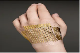
E-Skin has become the new emerging technology and also has great developing aspects as it is going to be one of the most futuristic projects to be enhanced and it also represents the next generation technology. This latest advance is an example of the progress in the field of micro fluidic stretchable radio frequency electronics (µFSRFE), which have demonstrated the possibility of combining established stiff electronic components with channels of elastomers filled with fluid metal. This design means it is possible to build systems that can return to their original after major mechanical deformation. This E-Skin could be used for a vast array of applications such as medical instruments that need to make controlled incision. Likewise, bandages could be equipped with sensors to ensure they are applied with proper tightness. Electronic pressure sensitive material that could become a sort of ―skin‖ Imitation for different applications. It was developed by engineers at Berkeley University of California. Artificial skin called ―e-skin‖ and described in an article published in the journal Nature Materials, is the first material of this kind, made of crystal inorganic semiconductors. The idea is of a material able to function like human skin, and this involves the integration capabilities of perception and touch objects. The team believes the sensors can act as a second layer of smart ‗e-skin ‗to monitor an individual‘s health.It is a thin material that contains electrical components and acts like a real skin in one or more ways. It could sense temperature, pressure, stretch and repair.The development of artificial skin is a hot research topic due to its relevant countless applications e.g. in robotics and in biomedical systems. It is an ultrathin electronic device that attaches to the skin which can measure electrical activity of heart, brain waves and other vital signals. Human skin provides sensory perception of temperature, pressure and air flow. Goal is to develop sensors on flexible substrates that are complaint to curved surfaces. Researcher‘s objective is for making an artificial skin is to make a revolutionary change in robotics, in medical field, in flexible electronics. Skin is large organ in human body so artificial skin replaces it according to our need. The main objective of artificial skin is to sense temperature, pressure, touch and whatever which human skin sense. It is a replacement for prosthetic and robotic arm.
E-Skin is also called as artificialskin. Some scientists call it as sensitive skin and synthetic skin. It is also called as fake skin. Such different names are available but the applications are same .It is used as a skin replacement for people who have suffered skin trauma. An artificial skin has also been demonstrated at the
Abstract:
The advancement of technology has enabled various approaches for developing artificial organ such as artificial ears, lungs and bionic eyes, etc. The best achievement as well as future example of integrated electronics in medical field is Electronic skin (e-skin). It can be used as skin replacement for people who have skin trauma such as skin disease or robotic applications. This paper focuses on the e-skinto build a skin work similar to that of the human skin and also it is embedded with several sensations or the sense of touch acting on the skin. This skin is already being stitched together. It consists of millions of embedded electronic measuring devices: thermostats, pressure gauges, pollution detectors, cameras, microphones, glucose sensors. This device would enhance the new technology which is emerging and would greatly increase the usefulness of robotic probes in areas where the human cannot venture. The sensor could pave the way for a overabundance of new applications that can wirelessly monitor the vitals and body movements of a patient sending information directly to a computer that can log and store data to better assist in future decisions. This paper offers an insight view of the designing, developing, implementing and usage of e-skin.University of Cincinnati for in-vitro sweat simulation and testing, capable of skin-like texture, wetting, sweat pore-density and sweat rates.
II.
System Structure and Implementation
The implementation of E-skin is illustrated in the following section.
A. Organic field effect transistors:
An organic field effect transistor (OFET) is a field effect transistor using an organic semiconductor in its channel. OFETs can be prepared either by vacuum evaporation of small molecules, by solution casting of polymers or small molecules, or by mechanical transfer of a peeled single-crystalline organic layer onto a substrate. These devices have been developed to realize low-cost, large-area electronic products and biodegradable electronics. OFETs have been fabricated with various device geometries. One of their main technological attractions is that all the layers of an OFET can be deposited and patterned at room temperature by a combination of low-cost solution- processing and direct-write printing, which makes them ideally suited for realization of low-cost, large-area electronic functions on flexible substrates.
B. Flexible array sensors:
Using organic transistors with a floating gate embedded in hybrid dielectrics that comprise a 2-nanometer-thick molecular self-assembled monolayer and a 4-2-nanometer-thick plasma-grown metal oxide, a nonvolatile memory arrays on flexible plastic substrates is prepared which is used in electronic skin. The small thickness of the dielectrics allows nonvolatile, reversible threshold-voltage shift. By integrating a flexible array of organic floating gate transistors with a pressure sensitive rubber sheet, a sensor matrix that identifies the distribution of applied mechanical pressure and stores the analog sensor input as a two-dimensional image over long periods of time is obtained
.
C. Nano wire arrays:
The nanowire arrays are made of germanium and silicon (semi conductors). The semiconductor nanowires enable fabrication of high performance, bendable transistors and sensors.
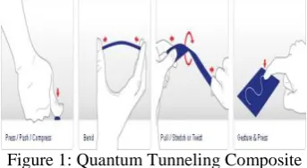
D. Quantum tunneling composite:
Quantum Tunneling Composite (QTC) is a new class of electrically conductive material that has been developed to advance the capability of switching and sensing systems as shown in figure 1. QTC is a pressure switching and sensing material technology. The QTC material can transits from an electrical insulator to a conductor due the deformation in material caused due to applied mechanical pressure
.
Figure 1: Quantum Tunneling Composite
E. Using Highly Sensitive Flexible Pressure Sensors with Micro-structured Rubber Dielectric Layers: The development of an electronic skin is critical to the realization of artificial intelligence that comes
into direct contact with humans, and to biomedical applications such as prosthetic skin depicted in figure 2.
A technology for the production of electronic skin needs to be reasonably priced and able to produce the skin with high throughput.
Need for a low-cost, large-area compatible technology for the production of pressure-sensitive pixels that are sensitive in both the medium pressure regime (10-100 kPa) to low-pressure regime (<10 kPa, gentle touch around 1kPa).
Flexible pressure sensors that utilizes the thin film capacitor and the organic field effect transistor device structures. The key component that enables the sensing of pressure in these devices is a thin dielectric layer of the biocompatible elastomer polydimethylsiloxane into which tiny structures has been molded.
Figure 2: Fabrication Rubber Dielectric Layers
F. Fabrication of E-skin
a. By using zinc oxide with vertical nanowires
Figure3:Zinc oxide with vertical nanowires e-skin
stating that it provides greater sensitivity and resolution. The system is based on piezoelectricity, a phenomenon that occurs when materials such as zinc oxide are pressed. Changes in the electrical polarization of the mass can be captured and translated into electrical signals thereby creating an artificial touch feeling.
b. By using Gallium Indium
The development of highly deformable artificial skin with contact force (or pressure) and strain sensing capabilities is a critical technology to the areas of wearable computing, haptic interfaces, and tactile sensing inmore autonomously and be more responsive to unexpected contacts by detecting contact forces during activities such as manipulation and assembly. Application areas include haptics humanoid robotics, and medical robotics.
Figure 4: By using Gallium indium (GaIn) e-skin
We describe the design, fabrication, and calibration of a highly compliant artificial skin sensor. The sensor consists of multilayered micro channels in an elastomeric matrix filled with a conductive liquid, capable of detecting multiaxis strains and contact pressure. A novel manufacturing method comprised of layered molding and casting processes is demonstrated to fabricate the multilayered soft sensor circuit. Silicone rubber layers with channel patterns, cast with 3-D printed molds, are bonded to create embedded micro channels, and a conductive liquid is injected into the micro channels. The channel dimensions are 200 μm (width) × 300 μm (height). The size of the sensor is 25 mm × 25 mm, and the thickness is approximately 3.5 mm. The prototype is tested with a materials tester and showed linearity in strain sensing and nonlinearity in pressure sensing. The sensor signal is repeatable in both cases. The characteristic modulus of the skin prototype is approximately 63 kPa. The sensor is functional up to strains of approximately 250%.
A highly elastic artificial skin was developed using an embedded liquid conductor. Three hyper-elastic silicon rubber layers with embedded micro channels were stacked and bonded. The three layers contain different channel patterns for different types of sensing such as multi-axial strain and contact pressure. A novel
manufacturing method with layered molding and casting techniques was developed to build a multi-layered soft sensor circuit. For strain sensing, the calibration results showed linear and repeatable sensor signal. The gauge factors of the skin prototype are 3.93 and 3.81 in x and y axes, respectively, and the minimum detectable displacements are 1.5 mm in x-axis and 1.6 mm in y-axis. For pressure sensing, the prototype showed repeatable but not linear sensor signals. The hysteresis level was high in a high pressure range (over 25 kPa). The sensor signal was repeatable in both cases.
c. By using Organic Transistors
By Nature Journal
In July they reported the success of our experiments in the journal Nature. They fabricated organic transistors and tactile sensors on an ultrathin polymer sheet that measured 1 micrometer thick—one-tenth the thickness of plastic wrap and light enough to drift through the air like a feather. This material can withstand repeated bending, crumple like paper, and accommodate stretching of up to 230 percent. What‘s more, it works at high temperatures and in aqueous environments—even in saline solutions, meaning that it can function inside the human body. Flexible electronics using organic transistors could serve a range of biomedical applications. For example, they‘ve experimented with electromyography, the monitoring and recording of electrical activity produced by muscles. For this system, they distributed organic transistor-based amplifiers throughout a 2-μm-thick film. This allowed us to detect muscle signals very close to the source, which is key to improving the signal-to-noise ratio, and thus the accuracy of the measurements. Conventional techniques typically use long wires to connect sensors on the skin with amplifier circuits, which results in a pretty abysmal signal-to-noise ratio. And they can imagine more medically urgent applications of such a system. In collaboration with the medical school at the University of Tokyo, we‘re working on an experiment that will place our amplifier matrix directly on the surface of an animal‘s heart. By detecting electric signals from the heart with high spatial resolution and superb signal-to-noise ratios, we should be able to zoom in on the exact location of problems in the heart muscle that can lead to heart attacks.
Skin is essentially an interface between your brain and the external world. It senses a tap on the shoulder or the heat from a fire, and your brain takes in that information and decides how to react. If we want bionic skins to do the same, they must incorporate sensors that can match the sensitivity of biological skins. But that is no easy task. For example, a commercial pressure-sensitive rubber exhibits a maximum sensitivity of 3 kilopascals, which is not sufficient to detect a gentle touch. To improve an e-skin‘s responsiveness to such stimuli, researchers are experimenting with a number of different techniques. Zhenan Bao and her colleagues at Stanford University created a flexible membrane with extraordinarily well touch sensitivity by using precisely molded pressure-sensitive rubber sandwiched between electrodes. A novel design of the thin rubber layer, using pyramid-like structures of micrometer size that expand when compressed, allowed the material to detect the weight of a fly resting on its surface. With such structures embedded in it, a bionic skin could sense a breath or perhaps a gentle breeze. This kind of sensitivity would be a great benefit in a prosthetic hand, for example, by giving the wearer the ability to grip delicate objects. In the most recent application of Bao‘s technology, her team turned the pressure sensors around so that instead of detecting external stimuli, they measured a person‘s internal functions. The researchers developed a flexible pulse monitor that responds to each subtle surge of blood through an artery, which could be worn on the inner wrist under a Band-Aid. Such an unobtrusive monitor could be used to keep track of a patient‘s pulse and blood pressure while in the hospital or during surgery.
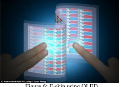
d. By Organic Light Emitting Diode
Figure 6: E-skin using OLED
and components that the researchers combined to make the light-emitting pressure-sensor array is impressive, says John Rogers, a professor of materials science at the University of Illinois at Urbana-Champaign. Rogers, whose group has produced its own impressive flexible electronic sensors (see ―Electronic Sensors PrintedDirectly on the Skin), says the result illustrates how research in nanomaterials is transitioning from the fundamental study of components and simple devices to the development of sophisticated, macro scale demonstrator devices, with unique function.‖ In this artist's illustration of the University of California, Berkeley's interactive e-skin, the brightness of the light directly corresponds to how hard the surface is pressed. Semiconducting material and transistors are fitted to flexible silicon to mimic pressure on human skin. The team is working on samples that respond to temperature. Scientists have created what's been dubbed the world's first interactive 'electronic skin' that responds to touch and pressure. When the flexible skin is touched, bent or pressed, built-in LED‘s light up - and the stronger the pressure, the brighter the light. The researchers, from the University of California, claim the bendy e-skin could be used to restore feeling for people with prosthetic limbs, in smart phone displays, car dashboards or used to give robots a sense of touch. Scientists from the University of California have created what's been dubbed the first 'electronic skin' that responds to touch and pressure by lighting up using built-in lights
.
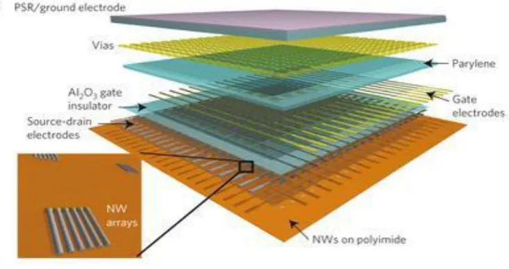
G. Using nano wires, sensor arrays rolled onto a polyimide base:
E-Skin is operated through a complex working principal and construction. The basic technology of the sensor material is a vast network of semiconductor nanowires as shown figure 7. These nanowires are made of germanium and they are rolled onto a polyimide base. This forms a substrate for a rubber film that, when pressure is applied, changes thickness. This change in material thickness is electrically measured through transistors and capacitors. Germanium and silicon are used in the nano wires. This material has good electrical properties and can thus operate at low voltages less than 5 volts. Using nano wires, sensor arrays rolled onto a polyimide base
:
Figure 7: Semiconductor Nanowires
H. A diagram of the construction layers required for E-Skin:
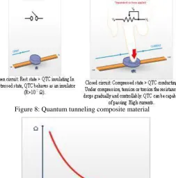
I. Using quantum tunneling composite material:
Quantum tunneling composite material has a feature of transiting from an electrical insulators into an conductor based on the influence of deformation in the material due to the result of applied mechanical pressure.QTC can be used to produce low profile, low cost, pressure activated switches or sensors that display variable resistance with applied force and return to a quiescent state when the force is removed. And the resistance range. The following figure 8, illustrate the QTC transition from an insulator into a conductor
.
Figure 8: Quantum tunneling composite material
Figure 9: Switching Performance
The Force (N) and Resistance (Ω) the transition from insulator to conductor follows a smooth and repeatable curve as shown in figure 9, with the resistance dropping exponentially. In theory, the resistance of QTC decreases exponentiallywith compression subsequently, allowing increasing current flow through the material. In practice uniform compression is rarely achieved and therefore the resistance alter with compression will diverge from a true exponential
.
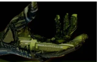
J. Robotic sensors implementing the E-skin technology
Figure 10: Example of E-Skin post Implementation
Scientists for the Department of Electrical Engineering and Computer Sciences of the University of California at Berkeley have created an electronic skin that can give robots an almost human sense of touch for them. Scientists have figured out how to give robots a sense of touch nearly as sensitive as that of humans. The electronic skin can distinguish extremely subtle texture differences far beyond the capabilities of current robotic. The E-skin is made of QTC material is durable, low cost, flexible integration using very small sensor material profile. The flexible E skin is more sophisticated. The above E-skin fabricated with the PDMS film substrate, flexible sensor arrays, nanowire arrays and the tactile sensors would sense the quantities like pressure and provide the sense of touch to the robot
.
III.
Conclusion
The artificial skin represents a new kind of material that uses an inorganic single crystalline semiconductor to mimic the touch-sensitivity of human skin. The researchers believe further development of this technology could restore the sense of touch in patients with prosthetic limbs. Further advances regarding the integration of electronic sensors with the human central nervous system are needed before this is made possible. Previous studies conducted to obtain artificial skin were based on organic materials, flexible and easy to treat, unfortunately, weak semiconductor materials are organic, which means that electronic devices built with them would require high voltage circuits to make it work. On the other hand, inorganic materials such as crystalline silicon and can operate at low voltages, in addition to being more stable and chemically. This time, the group of researchers at Berkeley has shown, however, that bands of inorganic materials miniature cables can be very flexible, ideal for making electronic circuits and sensors with high performance. In the near future, the scientists hope tocreate what they call e-skin, a second layer of skin that would move as a smart health monitoring gadget feature for humans. Thus E-skin would be the new and useful technology in the days to come.
Acknowledgment
I would like to thank Ms. M. Niranjana Priyadarshini, Assistant Professor, Department of ECE,PSNA College of Engineering and Technology.Dindigul for her continuous help and suggestions to improve the eminence of this paper.
References
[1]. http://hardware.slashdot.org/story/11/06/30/142249/Electronic-Skin
[2]. http://www.smartplanet.com/blog/science- scope/electronic- skin/6940
[3]. www.seas.harvard.edu/suo/papers/167.pdf [4]. www.pcworld.com
[5]. www.science20.com
[6]. www.nature.com/sifinder/10.1038/nmat2835
[7]. Kawai H. The piezoelectricity of PVDF. J. Appl. Phys. 1969;8:975–976.
[8]. Ikeda T. Fundamentals of Piezoelectricity. Oxford: Oxford Science Publications; 1996.
[9]. Singh M, Haverinen HM, Dhagat P, Jabbour GE. Inkjet printing – Process and Its Applications. Advanced Materials 2010;22:673-685.
[11]. Seminara L, Pinna L, Capurro M, Valle M. Smart Actuation and Sensing Systems: Recent Advances and Future Challenges. In: Berselli G, Vertechy R, Vassura G [Eds.]. Rijeka: InTech; 2012, pp. 611-638.
[12]. Dahiya RS, Cattin D, Adami A, Collini C, Barboni L, Valle M, Brunetti F. Towards tactile sensing system on chip for robotic applications. IEEE Sensors Journal 2011;11(12):3216-3226.
[13]. Dahiya RS et al. CMOS implementation of POSFET tactile sensing arrays with on chip readout. Fourth International Conference on Sensor Technologies and Applications (SENSORCOMM) 2010.
[14]. Caviglia S, Valle M, Bartolozzi C. Asynchronous, event-driven readout of POSFET devices for tactile sensing. Accepted for presentation at IEEE ISCAS 2014.