of the SiGe driver circuit for a silicon electro-optic ring modulator
A. Fatemi1, H. Gaul2, U. Keil2, and H. Klar1
1Institute of Microelectronics, Technical University of Berlin, Berlin, Germany 2FCI Deutschland GmbH, Berlin, Germany
Correspondence to: A. Fatemi (adel.fatemi@tu-berlin.de)
Received: 03 December 2014 – Revised: 09 June 2015 – Accepted: 18 June 2015 – Published: 3 November 2015
Abstract. This paper reports on a new SiGe driver IC to ad-dress the low breakdown voltage level of modern BiCMOS transistors. An optical modulator driver IC in SiGe 250 nm technology with a supply voltage of 4.5 V is presented. This driver IC consists of pre- and main driver stages where a newly modified cascode topology and capacitance degener-ation technique is employed to meet current applicdegener-ation re-quirements; high voltage swing at high datarate. The sim-ulation results show a differential output voltage swing of 3.9 Vp-p at 14 Gbps data rate, according to the FDR Infini-band standard.
1 Introduction
In recent years, many studies have worked to solve the band-width limitations of wire interconnection and the resulting cross talk in data communication. Photonics could be one way to solve this issue, even at higher transmission distances. By integrating optics into electronics, silicon phonic tech-nology promises to offer a higher level of integrity, greater bandwidth and lower energy consumption in data transmis-sion (Zuffada, 2012).
The optical modulator is a key element to implement the electrical-to-optical data conversion chain on the transmit-ter side. A micro-ring resonator, fabricated on a silicon sub-strate, is a high speed optical modulator (Zuffada, 2012). It maps voltage swing across its terminal to a specific level of optical output power. The proper Extinction Ratio (ER) is one of the main quality factors for optical modulation and is therefore dependent on the amplitude of the swing across the ring. Measurement results indicate (Giesecke et al., 2014) that voltage modulation must be in the range of 3–4 V to
provide an acceptable ER. Since a back plane electrical sig-nal could not directly fulfill this requirement (InfiniBand Ar-chitecture, 2012), an inter-stage broadband amplifier (here known as a driver IC) is needed to complete the electrical-to-optical conversion chain.
In broadband amplifier, Current Mode Logic (CML) con-figuration is typically used as the last stage of amplifier. Nowadays, with increasing transient frequency of modern BiCMOS transistors, their breakdown voltage capability is going to lower values (Mandegaran and Hajamiri, 2004). Therefore, obtaining high voltage swing in high transmission data rate is not straightforward.
In Sect. 2 of the present paper, a new modified cascode topology that divides all of the voltage stress among three transistors is explored, and a capacitance degenerative tech-nique that extends bandwidth is also reviewed. Driver IC de-signed in SiGe 250 nm technology will be explored in Sect. 3.
2 Design concept
2.1 Modified breakdown voltage doubler of bipolar transistors
Figure 1. The idea behind modified cascode topology.
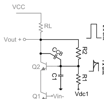
If the output voltage is at its maximum, it is desired to evenly divide the stress across two transistors in the case of similar devices in the stacks. A possible solution reported (Li et al., 2005a) is to use the intrinsic collector-base capacitance (CCB) of the upper transistor, Q2, to feed part of the output signal back to its base. In this way, both the base of the up-per transistor and its emitter follow the collector as shown in Fig. 2.
The precise analysis of the feedback network is not straightforward, as the influence of the feedback network and transistor, Q2, must be taken into account as is explained here (Li and Tsai, 2006). The simplified feedback network, with neglecting the effects of large base-collector ohmic re-sistance and other parasitic capacitances, can be modeled by C1, CCB, R1, and R2 as is highlighted in Fig. 3.
A resistive feedback network (R2 and R1) defines low fre-quencies of amplitude voltage of base of transistor, Q2, and C1 with collector-base capacitance provides voltage drop for higher frequencies. Choosing right value for C1 is quite im-portant as smaller capacitance brings some spikes at the base of the transistor and higher values of C1 limits the bandwidth as is shown in Fig. 3. It should be considered that R1 and R2 are chosen comparably larger than RL to reduce power con-sumption and have less influence on 50 ohm load impedance (Li and Tsai, 2006). Vdc controls the DC voltage of the base and emitter of Q2. Maximum single-ended output swing is calculated using the following equation:
1Vout=Vout,OFF−Vout,ON= 2×VCE,max+VCE,sat
−3×VCE,sat. (1)
In the present paper, the idea of using the intrinsic collector-base capacitance for the feedback network is extended into a
Figure 2. Modified cascode topology with feedback network and proper amplitude voltage ratio.
Figure 3. Simplified feedback network in half circuit differential mode.
three-stage cascode topology. This method can increase the maximum allowable output voltage swing while breakdown voltage is becoming less for upcoming downsized technolo-gies. Now, maximum single-ended output swing is calculated using the following equation:
1Vout=Vout,OFF−Vout,ON= 3×VCE,max+VCE,sat
−4×VCE,sat. (2)
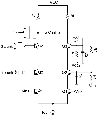
am-Figure 4. New modified multi-cascode topology with feedback net-work and corresponding voltage swing.
plitude. As is shown in Fig. 4, the feedback network must convey two-thirds, and one-third of the output signal for the base of Q2 and Q3 respectively, so as to drop one third of the whole output swing over each transistor. Here, the intrinsic collector-base capacitances, together with C1 and C2, pro-vide a high frequency feedback network for Q1 and Q2. 2.2 Capacitance degenerative technique
In a differential configuration pair, a capacitance degenera-tion technique could improve bandwidth by adding a pole and a zero to the system (Razavi, 2012). The zero is designed to coincide with and cancel the pole of the system, and the 3dB bandwidth is determined by the second pole, which is away from the first one.
Figure 5 shows how the pole and the zero are added to the CML in a differential configuration. For half of the cir-cuit in Fig. 5b, conductance of the common-emitter circir-cuit is (Razavi, 2012):
Gm=
gm
1+gm×
Rs
2|| 1+gm×Rs2
RS×CS
. (3)
If one assumes that the output pole of the differential pair is dominated byRL×CL, it would coincide with the added
zero to cancel each other out, only if:
RS×CS=RL×CL. (4)
Figure 5. (a) Capacitance degeneration technique, (b) half circuit in differential mode.
Figure 6. (a) Bandwidth of Gm, (b) overall system frequency re-sponse.
Therefore, overall bandwidth of the system is extended to the second pole of the system, (1+gm×Rs/2)/(RS×CS),
as shown in Fig. 6.
3 Design and implementation
Using the concepts discussed in Sect. 2, a driver IC was im-plemented in SiGe 250 nm technology. This driver IC con-sists of two parts: a pre-driver stage and a main driver stage. 3.1 Pre-driver stage
Back-plane electrical signals fall within a certain standard range. This range is normally not strong enough to com-pletely switch the current from one differential side to an-other one, a requirement for maximizing output swing and minimizing power consumption. In addition, a high ampli-tude input signal could bring the transistors into a deep sat-uration region where switching speed is reduced. Therefore, the pre-driver stage is placed before the main driver stage in order to prepare both the amplitude and the DC level of the input signal for the main stage driver IC.
Figure 7. Proposed pre-driver stage.
Figure 8. Proposed three stage cascode configuration.
for the common-emitter amplifier and cascade stage. In the present paper, the pre-driver output is designed to generate 500 mVp-p for the main driver stage.
3.2 Main driver stage
As target differential output swing is 4 Vp-p, supply volt-age is increased to 4.5 V. Figure 8 shows how the main stvolt-age driver IC is constructed, it consists of a three-stage cascode and capacitance degeneration technique. A simulated eye di-agram is depicted in Fig. 9, where its eye opening is 3.9 V at 14 Gbps.
Figure 10 shows how much voltage stress is on each de-vice. This figure indicates that stress is less than 1.5 V, which
Figure 9. Simulated eye diagram of output signal at 14 Gpbs.
Figure 10. Simulated collector-emitter voltage stress in multi-cascode topology.
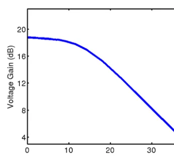
Figure 11. Simulated small signal voltage gain of driver IC.
third for high voltage swing application. Finally, the SiGe driver IC in 250 nm technology was investigated. Simulation results claim an output voltage swing of 3.9 Vp-p at 14 Gbps.
Acknowledgements. This work is funded by the Federal min-istry of education (BMBF) in the SHyWA project under Grant No. 16BP1103. The Author would like to thank Friedel Gerfers for his valuable discussions and guidance.
Edited by: D. Killat
Reviewed by: two anonymous referees
feedback networks, IEEE J. Solid-St. Circ., 1, 1025–1030, 2006. Li, D. U., Haung, L. R., and Tsai, C. M.: Low power consumption 10-Gbps SiGe modulator drivers with 9VPPdifferential output swing using intrinsic collector base capacitance feedback net-work, IEEE Rad. Freq. Integr., 1, 317–320, 2005a.
Li, D. U., Haung, L. R., and Tsai, C. M.: 10 Gbps CMOS laser driver with 3.3 V output swing, IEEE Cust. Integr. Cir., 1, 333– 336, 2005b.
Mandegaran, S. and Hajimiri, A.: A breakdown voltage doubler for high voltage swing drivers, IEEE Cust. Integr. Cir., 1, 103–106, 2004.
Rakowski, M., Ryckaert, J., Pantouvaki, M., Yu, H., Bogaerts, W., De Meyer, K., Steyaert, M., Absil, P. P., and Van Campenhout, J.: Low power, 10-Gbps 1.5-Vpp differential CMOS driver for a silicon electro-optic ring modulator, IEEE Cust. Integr. Cir., 1, 9–12, 2012.
Razavi, B.: Capacitance Degeneration, in: Design of Integrated Cir-cuit for Optical Communications, Second Edition, John Wiley and Sons, Hoboken, New Jersey, 140–143, 2012.