Vol.9 (2019) No. 2
ISSN: 2088-5334
Design of Energy Harvester Module with a Low RF Power Input for
UHF RFID Tag
Ula Grace Rosyidah
#, Trio Adiono
#,*1, Suksmandhira Harimurti
*, Amy Hamidah Salman
# #School of Electrical Engineering and Informatics Institut Teknologi Bandung, Jl. Ganesha 10, Bandung, 40132, Indonesia
*
University Center of Excellence on Microelectronics Institut Teknologi Bandung Jl. Tamansari 126, Bandung, 40132, Indonesia
E-mail: *1tadiono@stei.itb.ac.id
Abstract— An UHF RFID system is required to be able to operate at long range coverage, typically at 1-4 m. As a result, the RF signal
power received at RFID Tag is very low, typically at -10 dBm. Moreover, practically most of commercially used RFID Tag is passive, which means that it solely relies on the RF signal transmitted from the RFID reader as the power source. Therefore, it is mandatory and critical to design an efficient and low input power RFID Tag system. In this paper, an energy harvester module for UHF RFID Tag, which is able to work at low RF input signal power and generate a stable DC voltage output, is designed. The module is able to operate at a very low RF input power as low as -10 dBm or equal to 100 mVpeak of induced voltage. To obtain such performance, a modified and optimized rectifier-using a Dynamic Vth Cancellation technique, is designed. By using this technique, the rectifier is able to produce an efficient and a high output voltage. Additionally, bandgap reference and voltage regulator circuits are designed to be independent of power supply and temperature variation. As the result, a stable DC power supply output is able to be generated. All the circuits are designed on Silterra 130nm CMOS technology. This technology allows us to design the transistor to operate at a low threshold voltage of 0.1 V, which is very suitable for the application of low input power UHF RFID Tag system.
Keywords— UHF RFID; energy harvesting; dynamic Vth cancellation rectifier; bandgap reference; voltage regulator.
I. INTRODUCTION
Nowadays, the use of Radio Frequency Identification (RFID) system has been applied in various applications, such as stock inventory and logistics management system, access control, smart grid, and healthcare [1]-[3]. Besides, with the new paradigm of Internet of Things (IoT) technology, the use of RFID technology increases significantly. RFID, together with IoT, creates an innovation, called RAIN RFID, which allows the tagged items at different places can be monitored remotely via cloud [4]. Twenty eight million devices that apply this technology projected in 2020 [5].
In real practice, plenty of items or devices use a radio identification system at the same time. This may cause ambiguity or signal interference in the communication between Reader and Tag. Therefore, the RFID system needs to be developed by adding processor and security system. However, as a consequence, the addition of these features will increase the required power supply. The use of external power supply such as a battery is not preferred due to low efficiency, short lifetime, area consuming, high production cost, and packaging issue. To solve these issues, the system
must use an energy harvesting technique in generating the power supply. RFID Tag, which uses energy harvesting technique, is called a passive RFID tag [6]. Passive RFID Tag is a type of RFID Tag device that obtains the power solely from the incident radio frequency energy.
Therefore, in passive RFID Tag, it is required to design an energy harvester module. This module is responsible for converting the RF signal, sent by the reader, into a stable DC power supply. In this conversion, efficiency is a very crucial parameter to obtain a stable and sufficient power supply output level. The main circuit in the energy-harvesting module, which has the function to convert the RF signal into the DC signal, is rectifier. Several methods have been proposed to obtain a high-power efficiency rectifier. J. Yi et
al. [7] proposed a rectifier, using a diode-connected CMOS
highest efficiency is obtained by using Differential CMOS Rectifier or DVC. Additionally, in practical, RF signal received at the Tag antenna will vary depends on the distance between the Tag and Reader. In the worst case, the RF signal power may be very low, reaching -10dBm, which results in a low induced voltage at the Tag antenna, as low as 100 mV [11], [13]. In this work, the Silterra 130nm CMOS technology is used to utilize the 0.1 V threshold voltage (Vth) of the CMOS transistor. Furthermore, to obtain an efficient and high output voltage of the rectifier circuit, a modified and optimized DVC rectifier is designed. As previously stated that K. Lin.et al [12] has presented a high-efficiency rectifier circuit using DVC technique. However, a false configuration in using their rectifier design may result in a negative output of the rectifier, so that an additional set-up or circuit may be needed to address the issue. Here, we modify the rectifier, based on DVC technique, by flipping the position of the cross-coupled transistor, which results in a direct positive output of the rectifier.
Moreover, to meet the requirement of 0.1 V threshold voltage, we optimize the W/L size of the transistors in the rectifier circuit. By using the modified and optimized DVC rectifier, the energy harvester module can generate a stable DC output voltage of 2.27 V from an RF input with the peak signal is as low as 100 mV. The steady DC power supply of 1.8 V, which is also independent of power supply and temperature variation, is obtained by designing bandgap reference and voltage regulator circuits.
II. MATERIAL AND METHOD
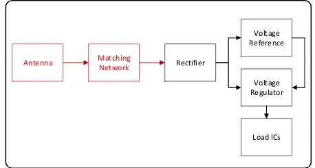
The energy harvester module consists of three main circuit blocks: rectifier, bandgap reference (BGR), and voltage regulator, as shown in Figure 1. The output of this energy harvester module will then be used as the power supply to the other circuit blocks, analog and digital blocks (load ICs). As illustrated in Figure 1 as well, aside of energy harvester module itself, a matching network is also required in designing an analog front-end circuit. The matching network has a function to increase the power transfer efficiency from the Tag antenna to the circuit blocks. However, this matching network will not be discussed in this paper since it is not the focus. The details of each circuit blocks of the energy-harvesting module are explained in the following subparts.
A. Rectifier
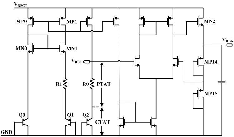
The rectifier is designed using the Dynamic Vth Cancellation (DVC) technique. The circuit configuration of our rectifier is shown in Figure 2. A discharge circuit is also added to the rectifier to avoid voltage overdrive [13]. As can be seen from Figure 2, for each stage, the PMOS transistors are placed on the right side, while the NMOS transistors are on the left side. By using this configuration, the rectifier can produce a positive voltage output directly.
The working principle of this rectifier is explained as follows. During positive half-cycles of the input signal,
• Node A experiences a positive voltage input, whereas node B is negative. Since the gate terminals of MN2 and MP2 are tied to Node A, MN2 turns on, and MP2 turns off. Reversely, since MP1 are tied to Node B, MP1 turns on, and MN1 turns off.
• A conduction path forms between the positive input terminal and the output node through CC1 and MP1. The
output storage capacitor is then charged to approximately
, 1
,pk C on
in
V
V
V
+
−
(1)Where:
Vin, pk = is the peak value of the input voltage
VC1 = is the voltage stored across CC1
Von = represents the voltage drop due to the
on-resistance of MP1.
It is assumed that CC1 is charged already to
approximately Vin, pk – Von during the preceding negative
half-cycle of the input signal.
• Another conduction path also forms between the negative input terminal and the ground node through CC2 and MN2.
The coupling capacitor CC2 is charged to approximately
Vin, pk – Von.
To obtain a 0.1 V threshold voltage of the transistors, W/L for PMOS is set to 2/0.13, while for NMOS is 6/0.13. By using this combination of W/L size, the rectifier is expected to produce the maximum voltage output at given input voltage as low as 100 mV.
Furthermore, in our design, to meet the requirement of the digital block, the rectifier has to be designed to produce an output DC voltage of more than or equal to 1.8 V. Therefore, the rectifier circuit itself has to be able to increase the voltage level to the required level. In our design, the rectifier is constructed in 4 stages to ensure a sufficient output DC level.
B. Bandgap reference and Regulator
Bandgap reference circuit is used to generate a reference voltage that is independent of temperature and power supply variation. Bandgap reference circuit generates two signals: Proportional to Absolute Temperature (PTAT) and Complementary to Absolute Temperature (CTAT) [14]. PTAT is generated by the natural response of the resistor, which produces a linear response of the voltage across the resistor as the temperature changes. On the other hand, CTAT is generated by the natural response of bipolar junction transistor (BJT) which produces a linear counter-response of the voltage across the base and emitter terminal (VBE) as the temperature changes. These two signals are then
summed up to provide a negligible output voltage change by the given temperature change, so-called a voltage reference.
Matching Network Rectifier Voltage Reference Voltage Regulator Load ICs Antenna
Fig. 2. Modified and Optimized Dynamic Vth Cancellation (DVC) Rectifier Circuit
Fig. 3. Bandgap Reference and Regulator Circuit
The bandgap reference circuit uses current mirror configuration to obtain an independent of power supply variation. The output of bandgap reference is expressed as follow:
)
(
1
,
n
N
V
V
V
iREF=
BE+
T (2)Where:
VBE = Base-Emitter voltage
x = ratio of resistor
VT = thermal voltage (approximately 26mV)
N = number of BJT
Accordingly, we design a bandgap reference circuit, which is independent of temperature change and power supply variation, as shown in Figure 3. Transistor MP0, MP1, MN0, MN1 is the current mirrors. BJT Q0 and Q1 are configured to work as a diode. Resistor R0 and BJT Q2 are the components that are responsible for generating the PTAT and CTAT signal.
RF signal at the Tag antenna will be at around -10dBm. This low and variation of the RF signal power is caused by the distance variation between the Tag and the Reader. A regulator is adopted in our design to prevent overvoltage, which can severely damage the transistor and other components. We use a regulator with Low Drop-Out (LDO)
topology, as shown in Figure 3. A differential op-amp, configured in error amplifier configuration, is employed in this design. The active loads (MP14 and MP15) divide rectifier output; the output of this voltage is then called as feedback voltage (VF). Both VF and VREF then become the
input of the amplifier. The difference between them is the error. The amplifier uses this error signal to generate a control signal for controlling the gate of MN2. As a result, the regulated voltage (VREG) is generated.
III.RESULTS AND DISCUSSION
All the circuits in this design are simulated using an input of -10dBm and in 50 Ohm system. The 50 Ohm system is chosen since most of the commercial antennas are using this system. In the 50 Ohm system, the -10dBm of RF signal input is approximately equal to 100 mV of voltage input received at the Tag antenna [11], [13]. The details of the simulation result for each circuit blocks are explained in the following subparts.
A. Rectifier Simulation
stable DC output voltage of 2.27 V can be obtained. It also has a fast time response, which is as low as 600 ns.
Fig. 4 Rectifier output
B. Bandgap Reference Simulation
Two simulations have been done for Bandgap reference to show its independence of power supply and temperature variation. These simulation results are shown in Figure 5 and 6. Figure 5 shows the simulation result of voltage reference output with the variation of power supply (VRECT). In this
simulation, the bandgap reference circuit is given a ramp input voltage from 1 V to 3 V. The simulation result shows that the bandgap reference can produce a stable voltage reference output of 1.16 V DC. Hence, it is proven that the bandgap reference circuit is independent of power supply variation.
Fig. 5. Voltage Reference Output with the Variation of Power Supply
Figure 6 shows the simulation result of voltage reference output with the variation of temperature. As explained in Part II. B, the bandgap reference circuit summed-up PTAT and CTAT signals. Hence, by summing-up these signals, the simulation proofs that the voltage reference output can be kept stable at 1.16 V DC regardless of the variation in temperature in the range of -40 to 120 °C.
Fig. 6. Voltage Reference Output with the Variation of Temperature
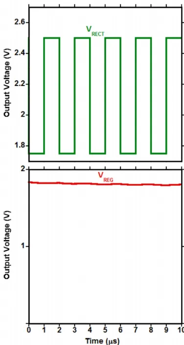
C. Regulator Simulation
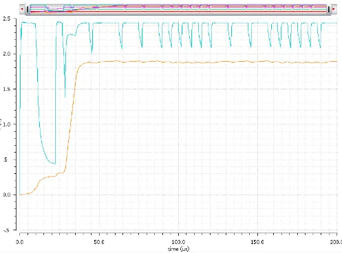
Figure 7 shows the simulation result of voltage regulator output with the input variation from the rectifier. In this simulation, the voltage regulator is given a rectangular pulse signal. The simulation result shows that the voltage regulator can produce a very stable DC output signal of 1.8 V. The simulation of the full circuit is shown in Figure 8.
Fig. 8. Simulation Result of Full Circuit Simulation
IV.CONCLUSION
An energy harvester module, which can operate at low RF power signal input, has been designed. It can work at RF power signal input of -10 dBm or approximately equal to 100 mV of induced voltage input. The modified and optimized DVC rectifier can generate a stable DC power of 2.27 V with a fast response time of 600 ns. By optimizing the design of band gap reference and voltage reference circuits, the energy harvester module can generate a stable DC power supply of 1.8 V, which is independent of power supply and temperature variation.
REFERENCES
[1] K. Jung and S. Lee, "A systematic review of RFID applications and diffusion: key areas and public policy issues," Journal of Open Innovation: Technology, Market, and complexity technology, Market, and Complexity, vol. 1, no. 9, Sep. 2015.
[2] S. Amendola, C. Occhiuzzi, and G. Marrocco, "RFID sensing networks for critical infrastructure security: A real testbed in a smart energy grid," in Proc. 2017 IEEE International Conference on RFID Technology & Application (RFID-TA), Sep. 2017, p. 106-110. [3] S.F. Wamba and E.W.T. Ngai, "Importance of issues related to
RFID-enabled healthcare transformation projects: results from a Delphi study," Production Planning & Control, vol. 26, no. 1, pp. 19-33, Oct. 2013.
[4] (2019) What is RAIN?. [Online]. Available: https://rainrfid.org/about-rain/what-is-rain/
[5] A. Shahrafidz Khalid, E. Conchon, and F. Peyrard, “Evaluation of RAIN RFID authentication schemes,” in Proc. 2016 Int. Conf. Cyber Security. Smart Cities, Ind. Control Syst. Commun. July 2007. [6] T. Adiono, A.H. Salman, Y.P. Yudhanto, N. Ahmadi, and S.
Harimurti, "Highly stable analog front-end design for NFC smart card," Analog Integr. Circ. Sig. Process., vol. 92, no. 1, pp. 71-79, Apr. 2017.
[7] J. Yi, W. H. Ki, and C. Y. Tsui, “Analysis and design strategy of UHF micro-power CMOS rectifiers for micro-sensor and RFID applications,” IEEE Trans. Circuits Syst. I Regul. Pap., vol. 54, no. 1, pp. 153–166, Jan. 2007.
[8] T. Umeda, H. Yoshida, S. Sekine, Y. Fujita, T. Suzuki, S. Otaka, "A 950-MHz rectifier circuit for sensor network tags with 10-m distance," IEEE J. Solid-State Circuits, vol. 41, no. 1, pp. 35–41, Jan. 2006.
[9] H. Nakamoto, D. Yamazaki, T. Yamamoto, H. Kurata, S. Yamada, K. Mukaida, et al., "A passive UHF RF identification CMOS Tag IC Using Ferroelectric RAM in 0.35-mm technology," IEEE J. Solid-State Circuits, vol. 42, no. 1, pp. 101–110, Jan. 2007.
[10] K. Kotani and T. Ito, "High-efficiency CMOS rectifier circuit with self-Vth-cancellation and power regulation functions for UHF RFIDs," in Proc. 2007 IEEE Asian Solid-State Circuits Conference (ASSCC’07), Nov. 2007, p. 119–122.
[12] K. Lin, B. Wang, X. Wang, J. Hou, C. Wang, X. Zhang, "A High-Efficient Energy Harvest Chain for Ultra-Low Power Passive UHF RRFID Tags," in Proc. 2014 12th IEEE International Conference on Solid-State and Integrated Circuit Technology (ICSICT 2014), Oct. 2014.
[13] D. J. Yeager, “Development and Application of Wirelessly-Powered Sensor Nodes,” M. S. thesis, University of Washington, Seattle, WA, USA, 2009.