Dr. S. Shirani COE2DI4 Midterm Test #2
Nov. 9, 2010
Instructions: This examination paper includes 11 pages and 20 multiple-choice questions starting on page 3. You are responsible for ensuring that your copy of the paper is complete. Bring any discrepancy to the attention of your invigilator. The answers for all the questions must be indicated by filling the corresponding circle on the optical scanning (OMR) examination sheet. This OMR examination sheet is the only page to be handed in. The instructions for completing the OMR examination sheet are provided on page 2. Read and follow these instructions with care! There is one mark for each question. Answer all questions. There is no penalty for guessing. This is a closed book exam. No reference material of any kind is permitted. No calculators of any kind are permitted. Time allowed is 50 minutes.
OMR examination instructions
NOTE: IT IS YOUR RESPONSIBILITY TO ENSURE THAT THE ANSWER SHEET IS PROPERLY COMPLETED: YOUR EXAMINATION RESULT DEPENDS UPON PROPER ATTENTION TO THESE INSTRUCTIONS.
The scanner, which reads the sheets, senses the bubble shaded areas by their
non-reflection of light. A heavy mark must be made, completely filling the circular bubble, with an
HB pencil. Marks made with a pen or felt-tip marker will NOT be sensed. Erasures must be thorough or the scanner may still sense a mark. Do NOT use correction fluid on the sheets. Do NOT put any unnecessary marks or writing on the answer sheet.
1. Print your name, student number, course name, section number, instructor name and the date in the spaces provided at the top of Side 1 (red side) of the sheet. Then you MUST sign the sheet in the space marked SIGNATURE.
2. Mark your student number in the space provided and fill in the corresponding bubble numbers underneath.
3. Mark only ONE choice from the alternatives (1,2,3,4,5 or A,B,C,D,E) provided for each question. If there is a True/False question, enter response of 1 (or A) as True, and 2 (or B) as False. The question number is to the left of the bubbles. Make sure that the number of the question on the scan sheet is the same as the question number on the test paper.
4. Pay particular attention to the Marking Directions on the form.
Multiple choice questions (numbered 1 to 20) –
indicate your answer by filling the
corresponding circle on the OMR answer sheet
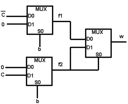
Figure 1 - Circuit for question 1.
1. The circuit show in Figure 1 is designed using two multiplexers. This circuit is equivalent to:
1. a positive edge triggered T flip flop 2. a negative edge triggered T flip flop 3. a negative edge triggered D flip flop 4. a positive edge triggered D flip flop 5. a 4-to-1 multiplexer
2. We would like to use a T flip flop and design a circuit that works like a J-K flip flop. The simplified input to the T flip flop should be:
1. T=J=K 2. T=JQ’+K’Q 3. T=JQ’+KQ 4. T=JQ+KQ’
5. We cannot build a J-K flip flop using a T flip flop
3. How many 4-to-1 multiplexers are needed to implement a 64-to-1 multiplexer?
1. 20 2. 18 3. 21 4. 16
4. How many 4-to-16 decoders are needed to implement an 8-to-256 decoder? Note, all the decoders have an enable input and all the inputs and outputs are un-inverted.
1. 2 2. 8 3. 9 4. 16 5. 17
5.What is the output, f(a,b,c,d), for the circuit of Figure 2?
1.
Σ
(1, 3, 6, 13) 2.Σ
(3, 13, 14)3.
Σ
(1, 3, 5, 6, 9, 10, 14) 4.Σ
(6, 10, 12, 15) 5.Σ
(1, 13)6. What is the output for the following circuit?
1. 2. 3. 4. 5.
[image:4.612.303.584.221.421.2]Figure 2 – Circuit for questions 5.
[image:4.612.310.522.509.681.2]7. What is the output for following circuit? 1. Z(t)=X(t)X(t-1).Z(t-1)
2. Z(t)=X(t)Z(t)Z(t-1) 3. Z(t)=X(t-1)Z(t)Z(t-1) 4. Z(t)=X(t)X(t-1)Z(t-2) 5. Z(t)=X(t-1)X(t-2)Z(t-2)
8. Which of the following statements is correct for the following circuit after using the shown clock?
1. Outputs for both flip flops will be 0. 2. Flip flops will swap their outputs. 3. Outputs for both flip flops will be 1.
[image:5.612.265.547.157.291.2]4. Outputs for both flip flops will be the same but indeterminable. 5. None of the above.
Figure 4 – Circuit for questions 7.
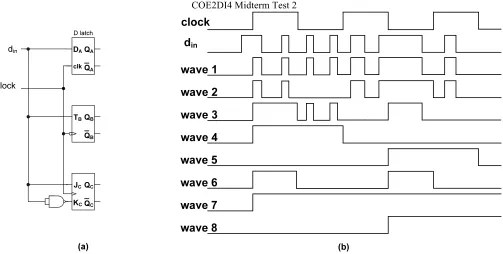
[image:5.612.87.253.401.574.2]Figure 6 - Sequential elements and output signal waveforms for questions 9, 10 and 11. Note, the sequential elements are assumed to be ideal, i.e., the propagation delay and setup and hold times are considered to be zero.
9. Given the clock and din waveforms in Figure 6(b) the waveform for QA from Figure 6(a) is:
1. wave 1 from Figure 6(b) 2. wave 2 from Figure 6(b) 3. wave 3 from Figure 6(b) 4. wave 4 from Figure 6(b) 5. wave 5 from Figure 6(b)
10. Given the clock and din waveforms in Figure 6(b) the waveform for QB from Figure 6(a) is:
1. wave 4 from Figure 6(b) 2. wave 5 from Figure 6(b) 3. wave 6 from Figure 6(b) 4. wave 7 from Figure 6(b) 5. wave 8 from Figure 6(b)
11. Given the clock and din waveforms in Figure 6(b) the waveform for QC from Figure 6(a) is:
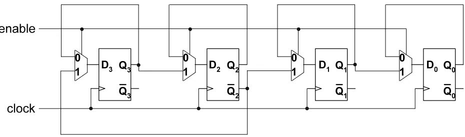
Figure 7 - Circuit for question 12.
12. In Figure 7, if enable=1 and the current (or present) state is Q3Q2Q1Q0=0101, then the next
state will be:
1. 1111
2. 1010
3. 1100
4. 0011
5. 0000
Figure 8 - Circuits for question 13 (it is assumed that after power up the state is 001).
13. Using an up counter with parallel load capability (Q2 and D2 are the most significant bits) we can generate a counting sequence 1, 2, 3, 4, 5, 6 using the circuit shown in:
1. Figure 8(a) 2. Figure 8(b) 3. Figure 8(c) 4. Figure 8(d)
[image:7.612.50.529.330.571.2]Figure 9 - Circuits for question 14 (it is assumed that after power up the state is 110).
14. Using a down counter with parallel load capability (Q2 and D2 are the most significant bits) we can generate a counting sequence 6, 5, 4, 3, 2 using the circuit shown in:
1. Figure 9(a) 2. Figure 9(b) 3. Figure 9(c) 4. Figure 9(d)
1. none of the above
15. Which of the circuits shown in Figure 10 are equivalent?
1. Figure 10(a) and Figure 10(c) only 2. Figure 10(a) and Figure 10(d) only 3. Figure 10(b) and Figure 10(c) only 4. Figure 10(b) and Figure 10(d) only 5. all of the above
Figure 11 - Implementations for function F(A,B,C) for question 16
16. Function F(A,B,C)=Σ m(0,7) can be implemented using A and B as the select (control) inputs to a 4-to-1 multiplexer. The correct implementation is:
1. shown in Figure 11(a) 2. shown in Figure 11(b) 3. shown in Figure 11(c) 4. shown in Figure 11(d) 5. none of the above
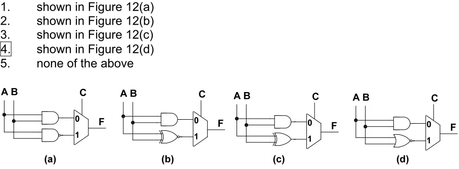
17. Function F(A,B,C)=Σ m(1,6) can be implemented using C as the select (control) input to a 2-to-1 multiplexer. The correct implementation is:
1. shown in Figure 12(a) 2. shown in Figure 12(b) 3. shown in Figure 12(c) 4. shown in Figure 12(d) 5. none of the above
[image:9.612.72.526.538.706.2]Figure 13 - Decoders without an enable signal for question 18
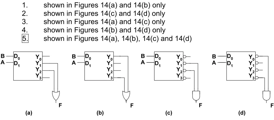
18. Figure 13 shows block diagrams and truth tables for decoders without an enable signal (Figure 13(a) for un-inverted outputs and Figure13(b) for inverted outputs). These decoders can be used for different implementations of function F(A,B)=Σ m(1,2), which are:
1. shown in Figures 14(a) and 14(b) only 2. shown in Figures 14(c) and 14(d) only 3. shown in Figures 14(a) and 14(c) only 4. shown in Figures 14(b) and 14(d) only
5. shown in Figures 14(a), 14(b), 14(c) and 14(d)
Figure 14 - Implementations for function F(A,B) for question 18
19. The single precision IEEE binary floating point representation for decimal number -0.75 is:
[image:10.612.36.490.335.535.2]20. Consider a carry look-ahead adder with two 8-bit operands A7A6A5A4A3A2A1A0
and B7B6B5B4B3B2B1B0 and an input carry C0. Then the logic equation for the output
carry is
C8=G7+P7G6+P7P6G5+P7P6P5G4+P7P6P5P4G3+P7P6P5P4P3G2+P7P6P5P4P3P2G1+
P7P6P5P4P3P2P1G0+P7P6P5P4P3P2P1P0C0, where the logic equations for carry
generate and carry propagate are Gi=AiBi and Pi=Ai+Bi respectively. We assume a
fan-in constraint of 3 and that the logic gates required for computing carry generate and carry propagate signals are not considered in the gate count for the logic used to implement the output carry C8. Then, to achieve the minimum propagation delay from
any input to C8, the minimum number of gates used to implement C8 is:
1. 14 gates (10 AND gates plus 4 OR gates) 2. 15 gates (11 AND gates plus 4 OR gates) 3. 19 gates (14 AND gates plus 5 OR gates) 4. 21 gates (16 AND gates plus 5 OR gates) 5. 23 gates (18 AND gates plus 5 OR gates)