VYSOKÉ UČENÍ TECHNICKÉ V BRNĚ
BRNO UNIVERSITY OF TECHNOLOGYFAKULTA ELEKTROTECHNIKY A KOMUNIKAČNÍCH TECHNOLOGIÍ
ÚSTAV MIKROELEKTRONIKY
FACULTY OF ELECTRICAL ENGINEERING AND COMMUNICATION DEPARTMENT OF MICROELECTRONICS
UNCONVENTIONAL CIRCUIT ELEMENTS FOR
LADDER FILTER DESIGN
DOKTORSKÁ PRÁCE
DOCTORAL THESIS
AUTOR PRÁCE
ING. MAHMOUD SHAKTOUR
AUTHOR
VEDOUCÍ PRÁCE
PROF. ING. DALIBOR BIOLEK, CSc.
SUPERVISOR
ABSTRACT
Frequency filters are linear electric circuits that are used in wide area of electronics. They are also the basic building blocks in analogue signal processing.
In the last decade, a huge number of active building blocks for analogue signal processing were introduced. However, there is still the need to develop new active elements that offer new possibilities and better parameters. The current-, voltage-, or mixed-mode analog circuits and their various aspects are discussed in the thesis. This work reflects the trend of low-power (LP) low-voltage (LV) circuits for portable electronic and mobile communication systems and the problems of their design. The need for high-performance LV circuits encourages the analog designers to look for new circuit architectures and new LV techniques.
This thesis presents various active elements such as Operational Transconductance Amplifier (OTA), Current Conveyor of Second Generation (CCII), and Current Differencing Transconductance Amplifier (CDTA), and introduces novel ones, such as Voltage Differencing Transconductance Amplifier (VDTA) and Voltage Differencing Voltage Transconductance Amplifier (VDVTA). All the above active elements were also designed in CMOS bulk-driven technology for LP LV applications.
This thesis is also focused on replacement of conventional inductors by synthetic ones in passive LC ladder filters. These replacements can lead to the synthesis of active filters with interesting parameters.
KEYWORDS
Analog signal processing, current-mode, voltage-mode, frequency filter, first-order all-pass filter, universal filter, KHN, active floating inductance simulator, OTA, CCII, CDTA, DVCC, VDTA, VDVTA.
ANOTACE
Kmitočtové filtry jsou lineární elektrické obvody, které jsou využívány v různých oblastech elektroniky. Současně tvoří základní stavební bloky pro analogové zpracování signálů.
V poslední dekádě bylo zavedeno množství aktivních stavebních bloků pro analogové zpracování signálů. Stále však existuje potřeba vývoje nových aktivních součástek, které by poskytovaly nové možnosti a lepší parametry. V práci jsou diskutovány různé aspekty obvodů pracujících v napěťovém, proudovém a smíšném módu. Práce reaguje na dnešní potřebu nízkovýkonových aplikací pro přenosné přístroje a mobilní komunikační systémy a na problémy jejich návrhu. Potřeba těchto výkonných nízkonapěťových zařízení je výzvou návrhářů k hledání nových obvodových topologií a nových nízkonapěťových technik.
V práci je popsána řada aktivních prvků, jako například operační transkonduktanční zesilovač (OTA), proudový konvejor II. generace (CCII) a CDTA (Current Differencing Transconductance Amplifier). Dále jsou navrženy nové prvky, jako jsou VDTA (Voltage Differencing Transconductance Amplifier) a VDVTA (Voltage Differencing Voltage Transconductance Amplifier). Všechny tyto prvky byly rovněž implementovány pomocí "bulk-driven" techniky CMOS s cílem realizace nízkonapěťových aplikací.
Tato práce je rovněž zaměřena na náhrady klasických induktorů syntetickými induktory v pasivních LC příčkových filtrech. Tyto náhrady pak mohou vést k syntéze aktivních filtrů se zajímavými vlastnostmi.
KLÍČOVÁ SLOVA
Analogové zpracování signálů, proudový mód, napěťový mód, kmitočtový filtr, fázovací článek 1. řádu, univerzální filtr, KHN, simulátor plovoucího induktoru, OTA, CCII, CDTA, DVCC, VDTA, VDVTA.
SHAKTOUR, M. Unconventional Circuit Elements for Ladder Filter Design:doctoral thesis. Brno: Brno University of Technology, Faculty of Electrical Engineering and Communication, Department of Microelectronics, 2011. 108 p. Supervised by prof. Ing. Dalibor Biolek, CSc.
DECLARATION
I declare that I have elaborated my doctoral thesis on the theme of “Unconventional Circuit Elements for Ladder Filter Design” independently, under the supervision of the doctoral thesis supervisor and with the use of technical literature and other sources of information which are all quoted in the thesis and detailed in the list of literature at the end of the thesis.
As the author of the doctoral thesis I furthermore declare that, concerning the creation of this doctoral thesis, I have not infringed any copyright. In particular, I have not unlawfully encroached on anyone‟s personal copyright and I am fully aware of the consequences in the case of breaking Regulation § 11 and the following of the Copyright Act No 121/2000 Vol., including the possible consequences of criminal law resulted from Regulation § 152 of Criminal Act No 140/1961 Vol.
Brno, 06. 04. 2011. ……….
Acknowledgments
I would like to express my gratitude to my supervisor, Prof. Dalibor Biolek, whose expertise, understanding, and patience, added considerably to my graduate experience. No teacher in my career has had a larger influence on my development than Prof. Dalibor Biolek. He has always had an open door for questions, comments, or discussions.
My thanks also goes to all those who have provided me with advice and assistance throughout my four years of doctoral study at the Brno University of Technology. Finally, I thank my family, especially my mother and father, my wife, Zayneb for their support during this process and throughout my life. Everything that I have and will accomplish is a direct reflection of their unending love and encouragement.
LIST OF ABBREVIATIONS
ABB Active Building Block AP All-Pass
BJT Bipolar Junction Transistor
BOTA Balanced-Output Operational Transconductance Amplifier BP Band-Pass
BS Band-Stop
CCII Second-generation Current Conveyor
CCII+/- Dual-Output Second-generation Current Conveyor CCs Current Conveyors
CDBA Current Differencing Buffered Amplifier
CDTA Current Differencing Transconductance Amplifier CDU Current Differencing Unit
CE Characteristic Equation CF Current Follower CM Current Mode
CMOS Complementary Metal Oxide Semiconductor DVCC Differential Voltage Current Conveyor FDNR Frequency Dependent Negative Resistor HP High-Pass
KHN Kerwin-Huelsman-Newcomb LP Low-Pass
MISO Multi-Input Single-Output
MOSFET Metal Oxide Semiconductor Field Effect Transistor OTA Operational Transconductance Amplifier
SIMO Single-Input Multi-Output SITO Single-Input Three-Outputs
SNAP Symbolic Network Analysis Program
SPICE Simulation Program with Integrated Circuit Emphasis VC Voltage Conveyor
VDTA Voltage Differencing Transconductance Amplifier
VDVTA Voltage Differencing Voltage Transconductance Amplifier VM Voltage Mode
LIST OF SYMBOLS
a, b coefficients of general transfer function
ai coefficients of non-cascade synthesis
C capacitance
D denominator of transfer function
f frequency
f0 characteristic frequency ϕ phase of all-pass filter
G conductance
gm transconductance of the OTA
R resistance
VDD, VSS supply voltages of CMOS structures
W/L CMOS transistor dimensions (Width / Length)
X, Y, Z+, Z– input or output, current or voltage terminals of the CCII Vin+, Vin-, Ioutinput or output, current or voltage terminals of the OTA
p, n, x+, x- input or output, current of the CDTA
Vp, Vn, x+, x- input or output, current or voltage terminals of the VDTA
Y admittance Z impedance
CONTEN
TS
1. State of the art ... 19
2. Thesis objectives ... 22
3. Active building blocks and their properties ... 23
3.1. Operational Transconductance Amplifier (OTA) ... 23
3.1.1. Operations using ideal OTA ... 24
Voltage Amplification using OTA ... 24
A Voltage –Variable Resistor (VVR) ... 24
Voltage summation using OTA ... 25
Integrator using OTA ... 26
3.1.2. CMOS Implementation of OTA ... 26
3.2. Current Conveyor of Second Generation (CCII) ... 27
3.2.1. Operations using the ideal CCII ... 29
Amplifiers using CCII ... 29
Integrators using CCII ... 29
Adders using CCII ... 30
Differentiators using CCII ... 31
3.2.2. Bulk-driven CCII± based on Bulk-driven OTA ... 31
3.2.3. Bulk-driven OTA with gm adjustable via external R ... 36
3.3. Current Differencing Transconductance Amplifier (CDTA) ... 41
3.3.1. Operations using the ideal CDTA ... 43
Integrator using CDTA ... 43
Current Summation using CDTA ... 43
3.3.2. CMOS Implementation of CDTA... 44
3.4. Voltage Differencing Transconductance Amplifier (VDTA) ... 49
3.4.1. Operations using the ideal VDTA ... 50
Current Summation using VDTA ... 51
3.4.2. CMOS Implementation of VDTA ... 51
3.5. Voltage Differencing Voltage Transconductance Amplifier (VDVTA) ... 53
3.6. Differential Voltage Current Conveyor (DVCC) ... 54
4. LC ladder simulation and other applications of active elements ... 57
4.1. Optimization of ladder filters with GmC simulation of floating inductors ... 57
4.1.1. MAX435 – a commercial OTA ... 57
4.1.2. Synthetic inductor based on MAX435 ... 57
4.1.3. LC Ladder simulation ... 59
4.2. Commercial active elements for filter implementation ... 65
4.2.1.Floating inductor replacement via “super-transistors” ... 67
4.2.2. Real properties of synthetic inductor ... 68
4.2.3. Utilizing synthetic inductors for LC ladder simulation ... 70
4.3. Floating GIC and its implementation... 73
4.3.1. Introduction ... 73
4.3.2. Proposed impedance converter ... 74
4.3.3. Analysis of the influence of parasitic impedances ... 75
4.3.3.1. Alternative model of impedance converter ... 75
4.3.3.2. Simulation of floating inductor ... 76
4.3.3.3. Simulation of floating capacitor ... 77
4.3.3.4. Simulation of the FDNR ... 78
4.3.4. Design example ... 79
4.4. Voltage Differencing Transconductance Amplifier for Filter Implementation ... 80
4.4.1. Synthetic inductor based on VDTA ... 81
4.4.2. Low-pass LC Ladder simulation ... 82
4.4.3. Band-pass LC Ladder simulation ... 85
4.4.5. Design of KHN filter using VDTA ... 90 5. Conclusion ... 94 6. Bibliography ... 96 7. Appendices ... 102 7.1. Appendix A ... 102 7.2. Appendix B ... 104
LIST OF FIGURES
Fig. 3-1: (a) OTA symbol, (b) ideal equivalent circuit. ... 23
Fig. 3-2: (a) Inverting and (b) noninverting voltage amplifier using OTA. ... 24
Fig. 3-3: Grounded voltage-variable resistor using OTA. ... 25
Fig. 3-4: Voltage summation using OTA. ... 25
Fig. 3-5: Integrators using OTA, (a) voltage-mode, (b) current-mode. ... 26
Fig. 3-6: Two stages Bulk-driven OTA [54]. ... 27
Fig. 3-7: (a) The CCII symbol, (b) ideal equivalent circuit. ... 28
Fig. 3-8: (a) CCII-based current amplifier, (b) CCII-based voltage amplifier. ... 29
Fig. 3-9: (a) CCII-based current integrator, (b) CCII-based voltage integrator. ... 29
Fig. 3-10: (a) CCII-based current adder, (b) CCII-based voltage adder. ... 30
Fig. 3-11: (a) CCII-based current differentiator, (b) CCII-based voltage differentiator. 31 Fig. 3-12: Bulk-driven CCII± based on Bulk-driven OTA. ... 32
Fig. 3-13: Frequency variation of the current gains IZ+/IX, IZ-/IX in dB of the CCII in Fig. 3-12. ... 32
Fig. 3-14: Voltage follower between X and Y of the CCII in Fig. 3-12. ... 33
Fig. 3-15: Current linearity between X and Y of the CCII in Fig. 3-12. ... 34
Fig. 3-16: The X node input resistance rin,x of the CCII in Fig. 3-12. ... 34
Fig. 3-17: The Z node output resistance rin,Z of the CCII in Fig. 3-12. ... 35
Fig. 3-18: (a) SISO OTA with gm adjustable, (b) DISO OTA with gm adjustable. ... 36
Fig. 3-19: Bulk-driven single input single output OTA (SISO) based on CCII. ... 37
Fig. 3-20: Bulk-driven fully differential OTA (DIDO) based on CCII and voltage buffer. ... 38
Fig. 3-21: DC transfer characteristics of bulk-driven fully differential OTA. ... 40
Fig. 3-23: (a) Symbol of the CDTA, (b) its implementation by bulk-driven OTAs. ... 42
Fig. 3-24: Integrator using CDTA. ... 43
Fig. 3-25: Current summation using CDTA. ... 43
Fig. 3-26: CMOS implementation of CDTA. ... 44
Fig. 3-27: DC curves Iz versus Ip or In, for Vz = 0. ... 46
Fig. 3-28: Frequency responses of current gains Iz/Ip and Iz/In for Vz = 0. ... 46
Fig. 3-29: DC curve Vp versus Ip for evaluating small-signal input resistance of the p- terminal. For the n-terminal, the result is identical. ... 47
Fig. 3-30: Frequency dependence of the impedances of p- and n- terminals. ... 47
Fig. 3-31: DC characteristics of OTA No. 3 with Rset linearization and transconductance control. ... 48
Fig. 3-32: Frequency responses of transconductances. ... 49
Fig. 3-33: (a) Symbol of the VDTA, (b) its implementation by OTAs. ... 50
Fig. 3-34: Integrator using VDTA. ... 51
Fig. 3-35: Current summation using VDTA. ... 51
Fig. 3-36: CMOS implementation of VDTA.. ... 51
Fig. 3-37: (a) Symbol of the VDVTA, (b) its implementation by OTA. ... 53
Fig. 3-38: CMOS implementation of VDVTA.. ... 51
Fig. 3-39: (a) DVCCII+ model, (b) DVCII+ using diamond transistors and buffer. ... 55
Fig. 3-40: Implementation of DVCII+ by current conveyor and by OTA. ... 56
Fig. 3-41: CMOS Implementation of DVCII+ by Bulk-driven current conveyor and by OTA. ... 56
Fig. 4-1: Synthetic inductor and the corresponding signal flow graphs. ... 58
Fig. 4-2: 5MHz lowpass ladder filter. ... 59
Fig. 4-3: Active ladder simulation by means of synthetic inductors and OTAs. ... 60
Fig. 4-5: PSpice analysis of synthetic inductors by means of dependences described by Signal- Flow-Graphs from Fig. 4-1, (a) before, (b) after optimizing the dynamic range. ... 63
Fig. 4-6: Frequency responses of ideal LC ladder (LC) and optimized active filter. ... 64
Fig. 4-7: (a) OTA, (b) CCII with nonzero x-terminal resistance, (c) „super-transistor“ as CCII, (d) „super-transistor“ with a degeneration RE resistance as single-input single-output OTA. ... 66
Fig. 4-8: Simulation of floating inductor. ... 67
Fig. 4-9: Model of the synthetic inductor in Fig. 5-8, with the real effects considered. 70
Fig. 4-10: 5MHz LC ladder filter. ... 71
Fig. 4-11: Active implementation of the filter from Fig. 5-10. Blocks „L1“ and „L2“ are synthetic inductors from Fig. 4-8. ... 71
Fig. 4-12: Frequency responses of the active filter from Fig. 4-11.. ... 72
Fig. 4-13: (a) Proposed impedance converter, (b) Parasitic impedances of active element. ... 74
Fig. 4-14: Model of the impedance converter from Fig. 4-13, with real effects taken into consideration. The black impedances in (b) are working, the remaining are parasitic. ... 76
Fig. 4-15: Simulation of the frequency dependence of the impedance of the synthetic floating capacitor. ... 80
Fig. 4-16: (a) Synthetic inductor circuit employing DISO OTA and SIDO OTA, (b) simplified representation of the synthetic inductor by VDTA. ... 81
Fig. 4-17: 25kHz LC ladder filter. ... 83
Fig. 4-18: Active implementation of the filter from Fig. 4-17. ... 83
Fig. 4-19: The frequency responses of ideal LC ladder and VDTA-based active filter. 84
Fig. 4-20: The group delay response of ideal LC ladder and VDTA-based active filter. ... 84 Fig. 4-21:The impedance values relative to frequency of the ideal and simulated inductors. ... 85
Fig. 4-22: Band-pass 8th order LC ladder filter.. ... 83
Fig. 4-24: The frequency responses of ideal LC ladder and VDTA-based active filter. 87
Fig. 4-25: The all-pass filter by OTAs. ... 88
Fig. 4-26: Implementation of all-pass filter in Fig. 4-25 by using VDVTA. ... 88
Fig. 4-27: Amplitude frequency responses of all-pass filters. ... 89
Fig. 4-28: Phase frequency responses of all-pass filters. ... 89
Fig. 4-29: Classical structure of the KHN filter. ... 90
Fig. 4-30: The corresponding flow-graph of KHN in Fig. 4-29. For R1 = R2 = R5 = R6, b2 = b1 = - b0 = 1. ... 90
Fig. 4-31: VDTA-based CM KHN circuit. ... 91
Fig. 4-32: The corresponding flow-graph of KHN in Fig. 4-31. ... 92
Fig. 4-33: Results of circuit simulations for CM KHN circuit using CMOS-based VDTAs. ... 93
LIST OF TABLES
3-1: Simulation results of the Bulk-driven OTA. --- 273-2: Simulation results of the Bulk-driven CCII. --- 35
3-3: Aspect ratios of the transistors used in the CCII. --- 39
3-4: Aspect ratios of the transistors used in the voltage buffer. --- 39
3-5:Variations of gm by Radj. --- 41
3-6: Simulation results of the Bulk-driven CDTA. --- 49 4-1:Parameters of elements of the synthetic inductors before and after optimization. - 62 4-2: Maximum values of inductor voltages and currents before and after optimization. 63
17
INTRODUCTION
Filters are widely used in analog signal processing [1] to select the particular frequency. Voltage-mode and current-mode circuits such as current conveyors [2] and current feed back operational amplifiers [3] are getting much attention as compared to other active elements due to wider bandwidth, simple circuitry, low power consumptions and dynamic ranges.
In the last decade, a huge number of active building blocks were introduced for analogue signal processing. However, there is still the need to develop new active elements that offer new and better advantages. This thesis is, therefore, focused on definition of other novel analog building blocks (ABBs) and, furthermore, novel filter structure designs.
In the present days, a number of trends can be noticed in the area of analogue filter and oscillator design, namely reducing the supply voltage of integrated circuits and transition to the current-mode [4]. On the other hand, current-, voltage- and mixed-mode analog circuits design still receives considerable attention of many researches. Therefore, the proposed circuits in this work are working in current-, voltage-, or mixed-mode.
This thesis work discusses the low-voltage analog active elements and their various aspects. The need of high speed, high performance, low power circuits because of the advent of the portable electronic and mobile communication systems and difficulties faced in achieving that in today, this need for high performance LV circuits give encourages the analog designers to look for new circuit architectures, and new LV techniques. Therefore the proposed circuits are implemented using bulk-driven CMOS structures.
The thesis is organized as follows: Chapter 3 presents various active elements. These active building blocks are further used in this thesis for various filters. This Chapter also introduces novel elements defined within this work. As applications, several current, voltage and mixed-mode filter structures utilizing: Operational Transconductance Amplifier (OTA), Current Conveyor of Second Generation (CCII), Current Differencing Transconductance Amplifier (CDTA), Voltage Differencing Transconductance Amplifier (VDTA), and Voltage Differencing Voltage Transconductance Amplifier (VDVTA) are presented in Chapter 4.
Chapter 4 is focused on replacement of conventional inductors by synthetic ones in passive LC ladder filters. It belongs to well-known methods of high-order low-sensitivity filter design. An efficient way of simulating the floating inductor consists in replacing the inductor by these active building blocks. Part of this Chapter focuses on such second-order filter structures that can provide all standard filter responses without changing the circuit topology.
18
Special attention is paid to Kerwin– Huelsman–Newcomb structure that enables independent control of the quality factor Q and characteristic frequency ω0.
To verify the behavior of the proposed circuits, defined active elements are implemented using bulk-driven CMOS structures.
19
1.
State of the art
In the last decade, a huge number of active building blocks (ABBs) were introduced for analogue signal processing.
Due to disadvantages of conventional inductors, active element-based inductor design is very desirable to designers today. During the last few decades, various floating inductors have been created using different high-performance active building blocks. That is why replacement of conventional inductors by synthetic ones in passive LC ladder filters belongs to well-known methods of high-order low-sensitivity filter design.
The current conveyor (CC) is the basic building block of a number of contemporary applications both in the current and the mixed modes. The principle of the current conveyor of the first generation was published in 1968 by K. C. Smith and A. S. Sedra [5]. Two years later, today‟s widely used second-generation CCII was described in [6], and in 1995 the third-generation CCIII [7]. However, initially, during that time, the current conveyor did not find many applications because its advantages compared to the classical operational amplifier (Op Amp) were not widely appreciated and any IC implementation of Current Conveyors was not available commercially as an off-the-shelf item.
Today, the current conveyor is considered a universal analog building block with wide spread applications in the current-, voltage-, and mixed-mode signal processing. Its features find most applications in the current mode, when its so-called voltage input y is grounded and the current, flowing into the low-impedance input x, is copied by a simple current mirror into the z output.
The demand for a multiple-output current conveyor led to the DO-CCII (Dual-Output CCII), which provides currents Iz of both directions, thus combining both the positive and the negative CCII in a single device [8]. If both currents are of the same polarity, the conveyors are of the CFCCIIp or CFCCIIn types (Current Follower CCII), where the symbol p or n means positive or negative current conveyor [9]. Another generalization is represented by the so-called DVCCII (Differential Voltage Current Conveyor) [10], in which the original “voltage” input y is split into a pair of inputs y1 and y2. The voltage of the x terminal is then given by the voltage difference of the voltage inputs. This offers more freedom during the design of voltage- and mixed-mode applications.
OTA (Operational Transconductance Amplifier) [11] belongs to the most widespread active elements for on-chip implementation of fast frequency filters.
20
It acts as a voltage-controlled current source with the possibility of electronic adjustment of transconductance gm.
Recently, the MO-OTA (Multiple Output OTA) has appeared as a generalization of BOTA (Bipolar OTA) and its applications in economical biquadratic filters [12], [13]. However, the drawbacks of such applications are not sufficiently emphasized. Some of them are referred to in [14]: the MO-OTA applications embody relatively high sensitivities to the attainable matching error of the current gains of the current mirrors that form the multiple output of the OTA.
Using the duality principle, the voltage conveyor (VC) has been presented in 1981 [15]. As in the theory of CCs, also here the first- and second-generation VCs (VCI, VCII, IVCI, and IVCII) were described [15], [16], [17], [18]. The best known VC is the plus-type differential current voltage conveyor (DCVC+) [19] that is more often labeled as the current differencing buffered amplifier (CDBA) [20].
By the modification of the CDBA or replacement of the VF (Voltage Follower) by the operational transconductance amplifier (OTA) [21], the current differencing transconductance amplifier (CDTA) [22] has been presented.
The methodology described, which uses the CDU (Current Differencing Unit) or CF (Current Follower) or CI (Current Inverter) as the input unit, and the following simple blocks such as voltage buffer, OTA, and CCII, represents an open system.
Continuing with the variation that the input unit will now implement voltage and not current differences, the Voltage Differencing Transconductance Amplifier (VDTA) has been introduced [23].
Recently, many papers were published about the simulation of passive ladder filters via numerous types of active elements. Direct simulation via inductor replacement by a synthetic element, indirect simulation via Bruton transformation of passive RCL cell and subsequent FDNR implementation, or leap-frog techniques was used.
In such circuits, frequently used active elements are CDBAs [24-26], CAs (Current Amplifiers) [27], MCCCIIs (Multi-Output CCCIIs) [28], CDTAs [29-31], OTRAs (Operational Transresistance Amplifier) [32], VCCs (Differential Voltage Current Conveyor) [33], CCIIs and CFAs [34], [35], DO_OTAs (Differential-Output OTAs) [36], MO_OTAs (Multiple-Output OTAs) [37], and a combination of classical Operational Amplifiers and OTAs [38]. Common drawback of the above circuit topologies consists in the circuit complexity. For example, a floating inductor is modeled via several active devices, and the
21
resulting filter structure contains large number of components, including floating resistors and capacitors. One exception from this rule is represented by recently introduced building block named CBTA (Current Backward Transconductance Amplifier) which enables simulating n-th order ladder filter via n CBTAs and n grounded capacitors [39], [40].
The above state-of-the-art clearly shows the topicality of the simulation of passive ladder filters via modern active elements as well as searching for such building blocks which would enable economical synthesis of artificial inductors. During the research activities towards finishing this work, it was shown that the VDTA element which was synthesized in the first stage of the research can be a good building block for designing economical ladder simulators.
22
2. Thesis objectives
The first aim of this thesis is to define various types of novel active building blocks for the effective synthesis of filter simulating RLC ladder structure. The second aim is to perform such a synthesis.
The first part of the thesis focuses on designing a high linearity, wideband bulk-driven OTA with tunable transconductance. This OTA is then used for designing active building blocks (CDTA, VDTA, VDVTA, and DVCC). As applications, several filters structures current-, voltage- and mixed-mode by using VDTA are presented, particularly the second-order filter structures that can provide all standard filter responses without changing the circuit topology. Special attention is paid to Kerwin–Huelsman–Newcomb structure that enables independent control of the quality factor Q and characteristic frequency ω0.
The second part of thesis deals with LC ladder simulation on the principle of inductor replacement by synthetic inductor.
The floating inductor is synthesized via:
1. MAX435, a commercial OTA [57], [64], which appears to be an optimal circuit element for such designs. Its differential input and output can be utilized for the simplification of the well-known circuitry for simulating the floating inductor. The transconductance of MAX435 is adjusted by an external two-terminal device. In the case of linear resistor, OTA has an extremely linear I&V characteristic. The limitations of the output current can be precisely set by another external resistor.
2. „super-transistor“ (S-T), which is commercially available in several versions, e.g. OPA615, SHC615, OPA860, and OPA861 [64].
3. Newly introduced VDTA and VDVTA elements [55]designed in the first part of the thesis. All the designs are verified in two steps:
In the first step, the theoretical analyses are done using SNAP software [41]. To verify the complex behavior of the proposed circuits, SPICE simulations are performed, utilizing transistor-level models of active elements.
23
3. Active building blocks and their properties
The following active elements are devices having multi ports with properties that make them useful in network synthesis [50]. Some active elements are more useful than others, depending of various design requirements.
3.1. Operational Transconductance Amplifier (OTA)
The OTAs were made commercially available for the first time in 1969 by RCA. The first publications with OTA came out in 1985, when authors in [21] presented to the general public the new CMOS OTA architectures and new filter realizations.
An ideal operational transconductance amplifier is a voltage-controlled current source, with infinite input and output impedances and frequency independent transconductance. OTA has two attractive features: 1) changing the external dc bias current or voltage can control its transconductance, and 2) It can work at high frequencies.
This research thesis focuses on the MOS implementations of the transconductance amplifiers.OTA is a voltage controlled current source.
More specifically, the term “operational" comes from the fact that it takes the difference of two voltages as the input for the current conversion. The ideal OTA is a differential-input voltage-controlled current source (DVCCS). Its symbol is shown in Fig. 3-1 (a), and its operation is defined by the following equation (3-1). Both voltages V+ and V- are with
reference to ground. The equivalent circuit of the ideal OTA is shown in Fig. 3-1 (b).
V+ V -Iout Ibias (a) Iout V+ V -+ -gm= (V+ - V-) (b) gm +
-Fig. 3-1: (a) OTA symbol, (b) ideal equivalent circuit.
24
Currently, the OTA elements are supplied on the market by many manufacturers [53].
A commercially available OTA elements are, for example, LT1228 (Linear Technology) or MAX435 (MAXIM-Dallas Semiconductor). The latter is a high-speed wideband transconductance amplifier (WTA) with high-impedance inputs and output. Due to its unique performance features, it is suitable for a wide variety of applications such as high-speed instrumentation amplifiers, wideband, high-speed RF filters, and high-speed differential line driver and receiver applications.
3.1.1. Operations using ideal OTA
Voltage Amplification using OTA
Inverting and noninverting voltage amplification can be achieved using an OTA as shown in Fig. 3-2 (a) and 3-2 (b), respectively [50]. Any desired gain can be achieved by a proper choice of gm and RL .It should be noted that the output voltage Vo is obtained from a source
with output impedance equal to RL. Zero output impedance can be achieved only if such
circuits are followed by a voltage follower.
+ -gm V+ V- Iout Vo RL + -gm Iout Vo RL Vo = - gmRL V -Vo = gmRL V+ (a) (b)
Fig. 3-2: (a) Inverting and (b) noninverting voltage amplifier using OTA.
A Voltage –Variable Resistor (VVR)
A grounded voltage-variable resistor can be easily obtained using an ideal OTA as shown in Fig. 3-3.Since Iout = -Iin, we have the following [50]:
25
+
-g
mV
-I
outV
oI
inI
out= - g
mV
_Z
inFig. 3-3: Grounded voltage-variable resistor using OTA.
Using two such arrangements cross-connected in parallel, a floating VVR can be obtained. On the other hand, if the input terminals in Fig. 3-3 are interchanged, the input resistance will be -1/gm. Thus, using OTAs, both positive and negative resistors become available without actually having to build them on the chip. These, coupled with capacitors, lead to the creation of the so called active-C filters.
Voltage summation using OTA
Voltage summation can be obtained using OTAs, which in effect translate voltages to currents. Currents are easily summed as shown in Fig. 3-4.
+
-g
m1V
1+I
in+
-g
m2V
2+I
in+
-g
m3I
outV
oI
out1I
out2Fig. 3-4: Voltage summation using OTA. It is clear that
(3-3)
26 (3-5) If gm1 = gm2 = gm3 (3-6)
By changing the grounded input of one of the input OTAs, voltage subtraction can be achieved. These operations are useful for the realization of filters which should be synthesized from their transfer functions.
Integrator using OTA
The operation of integration can be achieved very conveniently using the OTA as is shown in Fig. 3-5. The following equations can be written for Fig. 3-5 a) and b), respectively:
+
-C
g
mV
+V
-I
outV
o+
-C
g
mI
inI
out (a) (b)Fig. 3-5: Integrators using OTA, (a) voltage-mode, (b) current-mode.
( )
(3-7)
3.1.2. CMOS Implementation of OTA
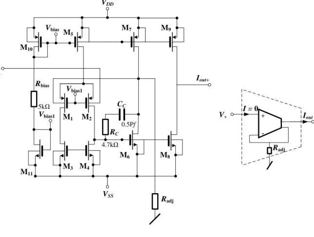
Bulk-driven CMOS implementation of OTA shown in Fig. 3-6 consists of two stage, the first which combined of the bulk-driven differential stage with pMOS input device M1 and M2 and
the current mirror M3 and M4 acting as an active load [54]. The second stage is a simple
CMOS inverter with M6 as a driver and M7 acting as an active load. Its output is connected to
the output of the differential stage by means of compensation capacitance Cc and the resistance RC since the compensation capacitance actually acts as a Miller capacitance in the
27
last stage. By setting the gate-source voltage to a value sufficient to turn on the transistor, then the operation of the bulk-driven MOS transistor becomes a depletion type.
R RC CC M1 M2 M3 M4 M5 M6 M7 VSS Vout Vbias Vbias1 Vbias1 M8 M9 V in-VDD Vin+
Fig. 3-6: Two stages Bulk-driven OTA [54].
Characteristics Simulation Result
Power consumption 30 μW
Open loop gain 70 dB
Bandwidth 4 MHz
Phase margin 70º
DC input voltage range -400, 700mV
Slow rate SRLH = 0.8V/μs , SRHL = 0.4V/μs
Measurement condition: VDD = 0.6V, VSS = 0.6V, CL = 1pF
Tab. 3.1: Simulation results of the Bulk-driven OTA.
3.2. Current Conveyor of Second Generation (CCII)
One of the most basic building blocks in the area of current-mode analogue signal processing is the current conveyor (CC). The principle of the current conveyor of the first generation was published in 1968 by K. C. Smith and A. S. Sedra [5]. CCI was then replaced by a more versatile second-generation device in 1970 [6], the CCII. Current conveyor designs
28
have mainly been with BJTs due to their high transconductance values compared to their CMOS counterparts. They are used as current-feedback operational amplifiers like the MAX477 high-speed amplifier and the MAX4112 low-power amplifier, which both feature current feedback rather than the conventional voltage feedback used by standard operational amplifiers.
Current conveyors are used in high-frequency applications where the conventional operational amplifiers can not be used, because the conventional designs are limited by their gain-bandwidth product.
The second-generation current conveyor (CCII) is used as a basic building block in many current-mode analog circuits. It is a three-terminal (X, Y and Z) device as shown in Fig. 3-7 (a), and the equivalent circuit of the ideal CCII is shown in Fig. 3-7 (b).
VX Y X Z VY IZ CCII 1 VY VX VZ (a) (b) VZ IY IX IZ
Fig. 3-7: (a) The CCII symbol, (b) ideal equivalent circuit.
The characteristics of ideal CCII are represented by the following hybrid matrix
[ ] [
] [ ] (3-8)
An ideal CCII has the following characteristics:
Infinite input impedance at terminal Y (RY = ∞ and IY = 0)
Zero input impedance at terminal X (RX = 0)
Accurate voltage copy from terminal Y to X (VX = VY)
Accurate current copy from terminal X to Z with infinite output impedance at Z (IZ =
29 3.2.1. Operations using the ideal CCII
Amplifiers using CCII
The CCII can easily be used to form the current output amplifiers and voltage-output amplifier as shown in Fig. 3-8. The voltage- and current- gains are as follows:
Y X Z CCII+ Iin Iout R2 R1 IX Y Z Y X X CCII CCII Vin Vout IX IZ R1 R2 Z (a) (b)
Fig. 3-8: (a) CCII-based current amplifier, (b) CCII-based voltage amplifier.
(3-9) (3-10)
Integrators using CCII
In Fig. 3-9, simple current- and voltage- integrators are presented.
Y Z Iin Iout R C X Y Z Vin R C X Y Z X Vout (a) (b) IX IZ CCII+ CCII CCII
30 The output signals are as follows:
(3-11)
(3-12)
Adders using CCII
In Fig. 3-10, CCII-based current adder and CCII-based voltage adder are reported, with the following equations:
I
in1I
in2X
Y
Z
I
out (a)X
Y
Z
V
in1X
Y
Z
V
in2I
1I
2R
1R
2R
V
out (b)I
ZCCII
CCII
CCII
Fig. 3-10: (a) CCII-based current adder, (b) CCII-based voltage adder.
( ) (3-13)
31 Differentiators using CCII
Current- and voltage-mode versions are shown in Fig. 3-11. The output signals are as follows:
Y X Z CCII Iin Iout R (a) C Y Z Z Y X X CCII CCII Vin Vout IX IZ (b) R C Fig. 3-11: (a) CCII-based current differentiator, (b) CCII-based voltage differentiator.
(3-15)
(3-16)
3.2.2. Bulk-driven CCII± based on Bulk-driven OTA
A new connection of Bulk-driven OTA is used to realize the CCII. In the OTA-based approach, presented in Fig.3-12, Bulk-driven OTA is used to implement the unity gain buffer between the Y and X inputs [54]. The X input current IX is sensed by duplicating buffers,
output transistors M6 and M7 using transistors M8 and M9, and extracting the X current from
them as IZ. Since transistors M8 and M9 have the same size and gate-source voltage as the
output stage transistors M6 and M7, the current IZ should be a copy of the current flowing
through M6 and M7 which is IX. Transistors M10-M15 are used to generate IZ. Since no
additional transistors need to be inserted between the OTA and rails, the approach will not increase the minimum operating voltage over that of the operational core. In addition the voltage follower is based on an OTA, thus it will maintain all the benefits and also the disadvantages of such a circuit i.e. a good voltage follower at the cost of lower bandwidth.
The simulated frequency responses of current gains Iz+/Ix, Iz-/Ix are given in Fig. 3-13. The
32 R RC CC M1 M2 M3 M4 M5 M6 M7 M8 M9 M10 M11 M12 M13 M14 M15 VSS Z+ Vbias Vbias1 Vbias1 M16 M17 Y Z -VDD X
Fig. 3-12: Bulk-driven CCII± based on Bulk-driven OTA.
Fig. 3-13: Frequency variation of the current gains IZ+/IX, IZ-/IX in Db of the CCII in Fig. 3-12. Frequency [Hz] 1.0Hz 10Hz 100Hz 1.0KHz 10KHz 100KHz 1.0MHz 10MHz 100MHz -10 -5 0 5 10 -15 Current gain [dB] Iz+/Ix Iz-/Ix
33
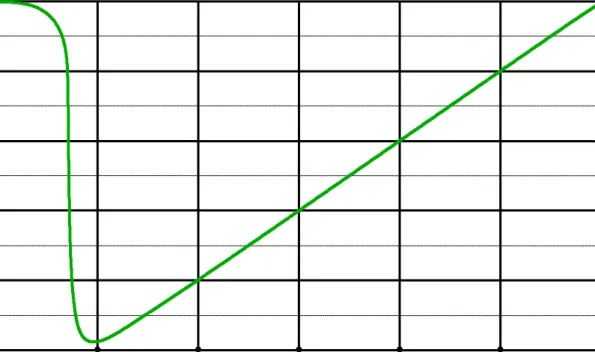
In Fig. 3-14, the input voltage buffer behavior is shown. A DC sweep simulation has been performed, to check the range in which the voltage on X node is equal to the voltage applied to Y node.
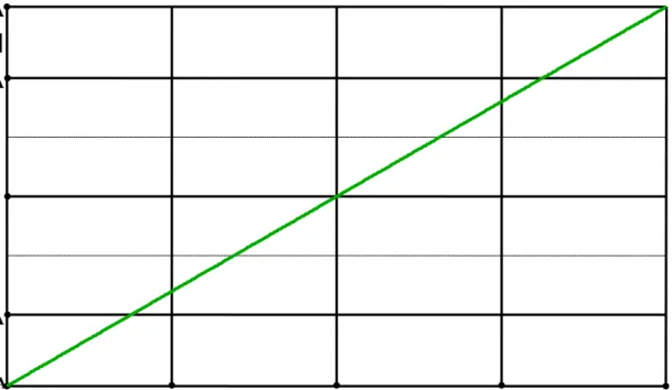
The current linearity between X and Y terminal of the bulk-driven current conveyor (CCII±) from Fig. 3-12, is demonstrated in Fig. 3-15. Note that for input currents Ix and Iz, the boundary of linear operation is ca ±16μA.
The corresponding small-signal current gains are as follows: Iz+/IX, Iz-/IX = 1, and the corresponding voltage gain VX/VY = 0.97.
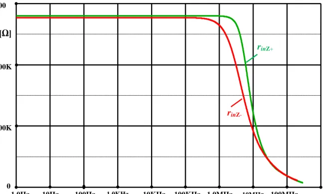
The small-signal low frequency resistance of the X terminal Rx is equal to166 Ω as shown
in Fig. 3-16. The small-signal resistance of the Y terminal RY is equal to 50GΩ. The small-
low frequency signal resistances of the Z+, Z- outputs terminals are equal to 560kΩ, and 554kΩ, respectively. Simulation results of the CCII± are summarized in Table 3-2.
Fig. 3-14: Voltage follower between X and Y of the CCII in Fig. 3-12.
-600mV -400mV -200mV 0mV 200mV 400mV 600mV -400mV -200mV 0V 200mV 400mV 600mV
VX[V]
VY[V]
34
Fig. 3-15: Current linearity between X and Y of the CCII in Fig. 3-12.
Fig. 3-16: The X node input resistance rin,x of the CCII in Fig. 3-12.
1.0GHz
Frequency
[Hz] 1.0Hz 10Hz 100Hz 1.0KHz 10KHz 100KH z 1.0MHz 10MHz 100MHz 0 5K 10K 15K 20K 24K RX[Ω]]-16uA -8uA 0A 8uA 16uA
-10uA 0A 10uA -16uA 16uA
I
X[A]
I
Z[A]
35
Fig. 3-17: The Z node output resistance rin,Z of the CCII in Fig. 3-12.
Characteristics Simulation Result
Power consumption 119 μW
3-dB bandwidth IZ+/IX 20 MHz
3-dB bandwidth IZ-/IX 52 MHz
DC voltage range -400, 600 mV
DC current range ±16 µA
Current gain IZ/IX 1
Voltage gain VX/VY 0.97
Node X parasitic DC resistance 166 Ω Node Y parasitic DC resistance 50 GΩ Node Z+ parasitic DC resistance 560 kΩ
Node Z- parasitic DC resistance 554 kΩ Measurement condition: VDD = 0.6V, VSS = - 0.6V
Tab. 3-2: Simulation results of the Bulk-driven CCII. Frequency [Hz] 1.0Hz 10Hz 100Hz 1.0KHz 10KHz 100KHz 1.0MHz 10MHz 100MHz 0 200K 400K RZ+- [Ω] 600 K rinZ+ rinZ-
36
3.2.3. Bulk-driven OTA with gm adjustable via external R
In this part, a new concept of high-linearity OTA with controllable transconductance is proposed. The OTA is simulated in a standard TSMC 0.18 mm CMOS process with a 0.6 V supply voltage.
The principle of gmadjustable via a feedback resistor Radj is show in Fig. 3-18.
+
-R
adj + 1 +-V
+I
outg
m, coreV
+I
outI = 0
I = 0
V
+V
-I
out +-R
adjV
+I
outI = 0
V
-(a) (b)Fig. 3-18: (a) SISO OTA with gm adjustable, (b) DISO OTA with gm adjustable.
In this part, a high linearity, wideband OTA with tunable transconductance is presented according to Eq. (3-18). The adjustable transconductance gm, adjust depends on Radj as follows:
37
Figs. 3-19, and 3-20 show circuit implementations of Fig.3.18, namely bulk-driven single input single output OTA (SISO) and a fully differential OTA (DIDO) based on voltage buffer and Current Conveyor of Second Generation CCII.
Radj Rbias RC CC M1 M2 M3 M4 M5 M6 M7 M8 M9 VSS 5kΩ 4.7kΩ 0.5Pf Iout+ Vbias Vbias1 Vbias1 M10 M11 V+ VDD + -Radj V+ Iout I = 0
Fig. 3-19: Bulk-driven single input single output OTA (SISO) based on CCII.
The aspect ratios of each of the transistors used the CCII and voltage buffer in Fig. 3-20 are listed in Tables 3-3 and 3-4, respectively.
38 Radj R1bias RC CC M1 M2 M3 M4 M5 M6 M7 M8 M9 M10 M11 M12 M13 M14 M15 VSS 5kΩ 4.7kΩ 0.5Pf CCII Iout+ Vbias Vbias1 Vbias1 M16 M17 V in-M18 M19 M20 M21 M22 RC1 CC1 M23 M24 VSS 4.7kΩ 0.5Pf Vbias Vbias1 Vin+ I out-VDD VDD 1 + -Radj Vin+ Iout+ Vin -I out-I = 0 Voltage Buffer
39
Transistor Length (µm) Width (µm)
M1,M2 2 30 M3,M4 2 4 M5,M16 3 20 M6,M8,M10,M12, M14 2 16 M7,M9,M11,M13, M15 3 40 M17 3 10
Tab. 3-3: Aspect ratios of the transistors used in the CCII in Fig. 3-20.
Transistor Length (µm) Width (µm)
M18,M19 2 30
M20,M21 2 4
M22 3 20
M23 2 16
M24 3 40
Tab: 3-4: Aspect ratios of the transistors used in the Voltage buffer in Fig. 3-20.
The performance of the proposed OTA in Fig. 3-20 was verified via PSPICE simulation. All the balanced CMOS OTA was simulated by using CMOS structure and MIETEC 0.18μm. The dimensions of transistors were used from Tables. 3-3 and 3-4 and the power supply voltages were set VDD= −VSS= ±0.6V.
Fig. 3-21shows the simulated transfer characteristics of the OTA in Fig. 3-20.The plots of the output current Iout versus the input voltage Vin show that, for Radj values of 1Ω, 10Ω,
100Ω, 1kΩ. 2kΩ, 5kΩ, 10kΩ, 20kΩ, 50kΩ, 100kΩ, 200kΩ, 500kΩ, and 1MΩ, the gm is controlled accordingly.
40
Fig. 3-21: DC transfer characteristics of bulk-driven fully differential OTA.
It is shown that the transconductance gain gm can be linearly tuned when Radj is increased. But for Radj bigger than 50kΩ it causes distortion. The linear range is very good for Radjof about 10kΩ.
The AC analysis of the bulk-driven OTA in Fig. 3.20 is shown in Fig. 3-22. The frequency dependence of Iout is measured by fixing AC value of Vin at 1V.
The responses are plotted for Radjof 1Ω, 10Ω, 100Ω, 1kΩ, 2kΩ, 5kΩ, 10kΩ, 20kΩ, 50kΩ, 100kΩ, 200kΩ, 500kΩ, and 1MΩ. The corresponding values of gmare shown in Table. 3-5
V
in -100mV -80mV -60mV -40mV -20mV -0mV 20mV 40mV 60mV 80mV 100mVI
out--10uA -5uA 0A 5uA 10uA Radj = 1Ω Radj = 1MΩ Radj = 10kΩ 100mV -100mV -80mV -60mV -40mV -20mV -0mV 20mV 40mV 60mV 80mVI
out+ -10uA -5uA 0A 5uA 10uAV
in Radj = 1Ω Radj = 1MΩ Radj = 10kΩ41
Fig. 3-22: AC transfer characteristics of bulk-driven fully differential OTA.
Radj gm 1Ω 2.2 ms 10Ω 2.16 ms 100Ω 1.8 ms 1kΩ 688.7 μs 2kΩ 408.5 μs 50 kΩ 184.45 μs 100 kΩ 96.82 μs 200 kΩ 50.1 μs 500 kΩ 21.04 μs 1 MΩ 11.2 μs
Tab: 3-5: Variations of gm by Radj.
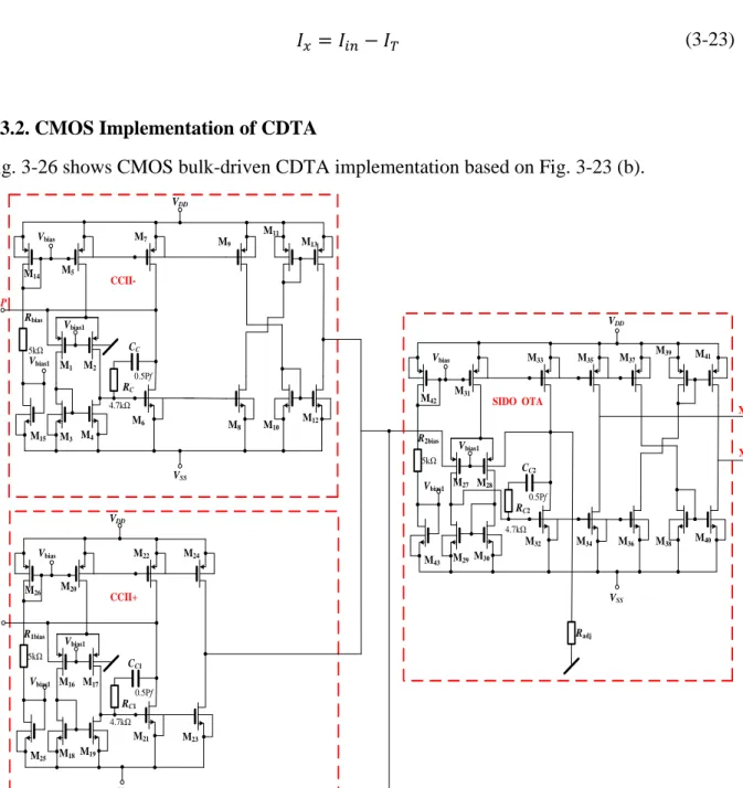
3.3. Current Differencing Transconductance Amplifier (CDTA)
The CDTA element [55] with its schematic symbol in Fig. 3-23 (a) has a pair of low-impedance current inputs p and n, and an auxiliary terminal z, whose outgoing current is the difference of input currents. Also in Fig. 3-23 (b) is given a possible implementation of
Frequency
1.0Hz 10Hz 100Hz 1.0KHz 10KHz 100KHz 1.0MHz 10MHz 100MHzI
out-0A 1.0mA 2.0mA 3.0mAI
out+42
CDTA using the OTA components. Here, output terminal currents are equal in magnitude, but flow in opposite directions, and the product of transconductance gm and the voltage at the z terminal gives their magnitudes. Therefore, this active element can be characterized with the following equations:
(3-18)
(3-19)
Where Vz = Iz.Zz and Zz is the external impedance connected to Z terminal of the CDTA.
CDTA can be thought as a combination of a current differencing unit [13] followed by a dual-output operational transconductance amplifier, DO-OTA. Ideally, the OTA is assumed as an ideal voltage-controlled current source and can be described by Ix = gm(V+ − V−), where Ix is
output current, V+ and V− denote non-inverting and inverting input voltage of the OTA,
respectively.
CDTA applications do not require the use of external resistors, which are substituted by internal transconductors. Analogously to the well-known “gmC” applications, the “CDTA-C”
circuits are formed by CDTA elements and grounded capacitors. Such structures are well-suited for on-chip implementation.
x-x+ p n x+ x-z Ix Ix Ip In Iz CDTA (a) n p + -z (b) + -+ - CCII -+ + + + Ip In Iz = Ip - In Ip In CCII+ OTA -Ip Radj 2 1 3
Fig. 3-23: (a) Symbol of the CDTA, (b) its implementation by bulk-driven OTAs.
Marking the voltages of p, n, x, and z terminals in Fig. 3-23 (a) with symbols Vp, Vn, Vx,
43 ( ) ( )( ) (3-20)
3.3.1. Operations using the ideal CDTA
Integrator using CDTA
The operation of integration can be achieved very conveniently using the CDTA as shown in Fig. 3-24. Clearly [56], (3-21) p n x+ x-z Ix Ix Ip In Iz= Ip CDTA C
Fig. 3-24: Integrator using CDTA.
Current Summation using CDTA
Current summation can be obtained using CDTA as shown in Fig. 3-25.
p
n
x+
x-z
I
xI
xI
inI
x+ I
TI
z= 0
CDTA
I
T44 We let z node outlet open, thus
(3-22)
(3-23)
3.3.2. CMOS Implementation of CDTA
Fig. 3-26 shows CMOS bulk-driven CDTA implementation based on Fig. 3-23 (b).
VDD Rbias RC CC M1 M2 M3 M4 M5 M6 M7 M8 M9 M10 M11 M12 M13 M14 M15 VSS 5kΩ 4.7kΩ 0.5Pf CCII-Vbias Vbias1 Vbias1 VDD R1bias RC1 CC1 M16 M17 M18M19 M20 M21 M22 M23 M24 VSS 5kΩ 4.7kΩ 0.5Pf CCII+ Vbias Vbias1 Vbias1 M26 M25 VDD Radj R2bias RC2 CC2 M27 M28 M29M30 M31 M32 M33 M34 M35 M36 M37 M38 M39 M40 M41 VSS 5kΩ 4.7kΩ 0.5Pf SIDO OTA X+ X-Vbias Vbias1 Vbias1 M42 M43 P Z n
45
The simulation results for the CDTA according to Fig. 3-26 are given in Figs. 3-27 to 3-32, and its small-signal parameters are summarized in Table 4-6.
Fig. 3-27 shows the Iz/Ip and Iz/In curves of the Current Differencing Unit (CDU), simulated on the assumption of Vz = 0. Note that for positive input currents Ip and In, the boundary of linear operation is ca 16μA. The current offset ∆Iz is ca -141 nA. For the bias point Ip = In = 0, the corresponding small-signal current gains are as follows: αp = Iz/Ip = 0.986,
αn =Iz/In = 1.
The frequency responses of current gains Iz/Ip, Iz/In are given in Fig. 3-28. The cutoff frequencies for the gains αpand αnare 22 MHz and 75 MHz, respectively.
The voltage-current characteristic of the p-terminal input gate of the CDTA is shown in Fig. 3-29. Identical results also hold for the n-terminal. Note that when the input current approaches a value of ca 17 μA, the clipping property of this curve can cause a significant nonlinear distortion. However, the range of linear operation is suitable for many applications that need extra low power consumption.
For the DC bias Ip = 0, the small-signal resistances Rp and Rn are 166 Ω. The frequency
dependences of the impedances of p- and n- terminals in Fig. 3-30 show that the above values are kept up to ca one hundred kilohertz. Then the impedances increase due to the frequency dependence of the OTA transconductances.
46
Fig. 3-27: DC curves Iz versus Ip or In, for Vz = 0.
Fig. 3-28: Frequency responses of current gains Iz/Ip and Iz/In for Vz = 0.
Frequency
[Hz] 1.0Hz 10Hz 100Hz 1.0KHz 10KHz 100KHz 1.0MHz 10MHz 100MHz -20 -16 -12 -8 -4 0 4 IZ/Ip IZ/In [dB]-20uA -16uA -12uA -8uA -4uA 0uA 4uA 8uA 12uA 16uA 20uA
-20uA -10uA 0 A 10uA 20uA Ip In Ip,In [A] IZ [A]
47
Fig. 3-29: DC curve Vp versus Ip for evaluating small-signal input resistance of the p- terminal. For the n-terminal, the result is identical.
Fig. 3-30: Frequency dependence of the impedances of p- and n- terminals.
Frequency
[Hz] 1.0Hz 10Hz 100Hz 1.0KHz 10KHz 100KHz 1.0MHz 10MHz 100MHz 500MHz 0 2kΩ 4kΩ 6kΩ 8kΩ 10kΩ Rp,n[Ω]-20uA -16uA -12uA -8uA -4uA 0A 4uA 8uA 12uA 16uA 20uA -150m -100m -50m 0m 50m Vp [V]
48
The Ix versus Vz curves in Fig. 3-31 are analyzed for several values of the external resistance Rset. They clearly show the transconductance control via Rset as well as the effect of the linearization and increasing the dynamic range with increasing values of Rset. A detailed analysis also confirms that the current offset is decreasing with increasing value of Rset. For
Rset = 10 kΩ, the offset current is only -141 nA. Fig. 3-32 shows the frequency dependences of gm,set and of the x- and z-terminal impedances. The transconductance bandwidth increases with increasing Rset. For example, Rset = 10 kΩ yields gm,set ≈ 99 μA/V and the -3dB cutoff
frequency is approximately 1.1 MHz. The frequency dependence of the z-terminal impedance shows the value 277 kΩ, with a -3dB cutoff frequency of about 2 MHz. The low-frequency x -terminal resistance is ca 554 kΩ. Simulation results of the CDTA are summarized in Table 3-6.
Fig. 3-31: DC characteristics of OTA No. 3 with Rset linearization and transconductance control. -100mV -75mV -50mV -25mV 0mV 25m VV 50mV 75mV 100mV 0 A -25uA 25uA Rset :100kΩ 50kΩ 20kΩ 10kΩ 5kΩ IX+ IX-VZ [V] IX [A]
49
Fig. 3-32: Frequency responses of transconductances.
Characteristics Simulation Result
Power consumption 264 µW
3dB bandwidth IZ/Ip, IZ/In 22 MHz, 75MHz DC current range Ip, In ±16 µA
DC voltage range VZ(Rset =10kΩ) +170 mV, -310 mV
DC offset of OTA stage (Rset =10kΩ) -141 nA
Current gains IZ/Ip, IZ/In 0.986, 1
gm (Rset =10kΩ) 98.9 µA/V
3dB bandwidth gm (Rset =10kΩ) 1.2 MHz
Node n and p parasitic DC resistance 166 Ω Node z parasitic DC resistance 277 kΩ Node x parasitic DC resistance 554 kΩ
Measurement condition: VDD = 0.6V, VSS = 0.6V
Tab. 3-6: Simulation results of the Bulk-driven CDTA.
3.4. Voltage Differencing Transconductance Amplifier (VDTA)
The methodology described in the CDTA, which uses the CDU as the input unit, and the following simple block OTA represents an open system: Let us continue with the variation that the input unit will now implement voltage and not current differences. The differential-input OTA is a simple element for realizing the voltage difference. Simultaneously, it can
Frequency
[Hz] 1.0Hz 10Hz 100Hz 1.0KHz 10KHz 100KHz 1.0MHz 10MHz 100MHz 0 50 100 150 200 Rset =5kΩ Rset =10kΩ Rset =20kΩ Rset =50kΩ Rset =100kΩ gm,set[µA/V]50
provide the possibility of electronic control. The VDTA element [23] with its schematic symbol in Fig. 3-33 (a)has a pair of high-impedance current inputs p and n, and an auxiliary terminal z. A multiple copies of Iz current are indicated here in order to increase the
universality of VDTA element. Thus, according to the proposed methodology, the VDTA element should have the “zc“(Z Copy) attribute. Also a possible implementation of VDTA using two OTA components is given in Fig. 3-33 (b). Here, output terminal currents are equal in magnitude, but flow in opposite directions, and the product of transconductance (gm) and the voltage at the z terminal gives their magnitudes. Therefore, this active element can be characterized with the following equations:
( ) (3-24)
(3-25)
(3-26)
VDTA has an interesting application potential: for example, the floating loss-less inductor can be simulated only by one VDTA and one grounded capacitor.
p n x+ x-z VDTA Ix Ix Iz Ip = 0 In = 0 Vp Vn Vp n p gmx+ -OTA2 x+ x-gmz OTA1 Vn 0A 0A z zc Iz = gmz (Vp – Vn) Izc = ±Iz + -+ Ix Ix (a) (b) zc Izc
Fig. 3-33: (a) Symbol of the VDTA, (b) its implementation by OTAs.
3.4.1. Operations using the ideal VDTA
Integrator using VDTA
The operation of integration can be achieved very conveniently using the VDTA as is shown in Fig. 3-34. Clearly,
![Fig. 3-6: Two stages Bulk-driven OTA [54].](https://thumb-us.123doks.com/thumbv2/123dok_us/1871383.2773132/27.892.239.664.218.614/fig-two-stages-bulk-driven-ota.webp)