BRNO UNIVERSITY OF TECHNOLOGY
VYSOKÉ UČENÍ TECHNICKÉ V BRNĚFACULTY OF ELECTRICAL ENGINEERING AND
COMMUNICATION
DEPARTMENT OF CONTROL AND
INSTRUMENTATION
FAKULTA ELEKTROTECHNIKY A KOMUNIKAČNÍCH TECHNOLOGIÍ
ÚSTAV AUTOMATIZACE A MĚŘICÍ TECHNIKY
CHARGE CONTROLLER FOR SOLAR PANEL BASED
CHARGING OF LEAD-ACID BATTERIES
REGULÁTOR PRO NABÍJENÍ OLOVĚNÝCH AKUMULÁTORŮ Z FOTOVOLTAICKÉHO PANELU
MASTER’S THESIS
DIPLOMOVÁ PRÁCEAUTHOR
Bc. PETER KORENČIAK
AUTOR PRÁCE
SUPERVISOR
doc. Ing. PETR FIEDLER, Ph.D.
VEDOUCÍ PRÁCE
ABSTRACT
This thesis deals with the design and implementation of a charge controller for multiple lead-acid batteries to be used in a solar system. Such controller enables an independent connection and charge control for each of more batteries with possibly different age and parameters. It is in contrast with solutions with one connection for multiple batteries connected in parallel, where mixing different battery types or ages is not recommended. This controller offers very high scalability of energy storage in solar system. It is also possible to use older batteries together with new ones instead of having to replace the old batteries when their capacity falls below required level.
The requirements, hardware and software design along with the implementation of such controller with 20A nominal output current for five 12V lead-acid batteries are discus-sed in detail in this thesis. Additional features, alternative designs and algorithms are discussed as well. An important part of the work concentrates on high current switch design, short circuit protection as well as circuit for DC current measurement. Correct functionality of the implemented controller has been verified by measurements.
KEYWORDS
charge controller, charging, multiple lead-acid batteries, photovoltaic panel, solar system
ABSTRAKT
Tato diplomová práce se zabývá návrhem a realizací regulátoru pro použití v solárním systému s větším počtem olověných akumulátorů. Takový regulátor umožňuje nezávislé připojení a řízení nabíjení většího počtu akumulátorů různého stáří a parametrů. To je v kontrastu s řešeními obsahujícími jedno připojení pro více baterií připojených paralelně, kde se míchání baterií různého druhu a stáří nedoporučuje. Tento regulátor nabízí vysokou škálovatelnost skladování energie v solárním systému. Umožňuje také používat starší baterie s novými, místo nutnosti staré baterie nahradit, když jejich kapacita klesne pod požadovanou úroveň.
V této práci jsou podrobně popsány požadavky, návrh hardwaru a softwaru a implemen-tace regulátoru s nominálním výstupním proudem 20A pro pět 12V olověných baterií. Práce popisuje také další funkce, stejně jako alternativní návrhy a algoritmy. Důležitá část práce se zabývá designem spínačů pro velké proudy, ochrany proti zkratu a obvodů pro měření stejnosměrného proudu. Správná funkčnost regulátoru byla ověřena měřením.
KLÍČOVÁ SLOVA
regulátor nabíjení, nabíjení, vícero olověných akumulátorů, fotovoltaický panel, solární systém
KORENČIAK, P.Charge controller for solar panel based charging of lead-acid batteries. Brno: Brno University of Technology, Faculty of Electrical Engineering and Communi-cation, 2011. 89 p. Master’s thesis supervised by doc. Ing. Petr Fiedler, Ph.D.
DECLARATION
I declare that I have elaborated my master’s thesis on the theme of “Charge controller for solar panel based charging of lead-acid batteries” independently, under the supervision of the master’s thesis supervisor and with the use of technical literature and other sources of information which are all quoted in the thesis and detailed in the list of literature at the end of the thesis.
As the author of the master’s thesis I furthermore declare that, concerning the cre-ation of this master’s thesis, I have not infringed any copyright. In particular, I have not unlawfully encroached on anyone’s personal copyright and I am fully aware of the consequences in the case of breaking RegulationS11 and the following of the Copyright Act No 121/2000 Vol., including the possible consequences of criminal law resulting from regulations in part two, chapter VI., volume 4 of Criminal Act No 40/2009 Vol.
PROHLÁŠENÍ
Prohlašuji, že svou diplomovou práci na téma „Regulátor pro nabíjení olověných aku-mulátorů z fotovoltaického panelu“ jsem vypracoval samostatně pod vedením vedoucího diplomové práce a s použitím odborné literatury a dalších informačních zdrojů, které jsou všechny citovány v práci a uvedeny v seznamu literatury na konci práce.
Jako autor uvedené diplomové práce dále prohlašuji, že v souvislosti s vytvořením této diplomové práce jsem neporušil autorská práva třetích osob, zejména jsem nezasáhl nedo-voleným způsobem do cizích autorských práv osobnostních a jsem si plně vědom následků porušení ustanoveníS11 a následujících autorského zákona č. 121/2000 Sb., včetně mož-ných trestněprávních důsledků vyplývajících z ustanovení části druhé, hlavy VI. díl 4 Trestního zákoníku č. 40/2009 Sb.
Brno . . . . (podpis autora)
ACKNOWLEDGEMENT
I would like to express my deepest gratitude to my advisor doc. Ing. Petr Fiedler, Ph.D. for his helpful comments, suggestions and guidance throughout the work on this thesis. I thank my parents for their support during my studies and to Ing. Miloš Caha for his suggestions, designing the board layout and producing the printed circuit boards for the prototype of the charge controller.
Brno . . . . (author’s signature)
CONTENTS
Introduction 11 1 Requirements 13 1.1 Lead-Acid Batteries . . . 13 1.1.1 Background . . . 13 1.1.2 Types . . . 13 1.1.3 Issues . . . 14 1.1.4 Charging . . . 15 1.2 Considered Functionality . . . 16 1.3 Block Diagram . . . 191.3.1 Preliminary Block Diagram . . . 19
1.3.2 Updated Block Diagram . . . 20
1.4 Definition of Design Requirements for Building Blocks . . . 20
2 Hardware Design 25 2.1 Design of Fundamental Building Blocks . . . 25
2.1.1 Power Switch and Power Switch Control . . . 25
2.1.2 Current Measurement . . . 35
2.1.3 Voltage Measurement . . . 38
2.1.4 Short Circuit Protection . . . 43
2.1.5 Microcontroller . . . 43
2.1.6 Voltage Regulator . . . 45
2.1.7 Protection Against Reverse Battery Connection . . . 46
2.1.8 Thermal Protection . . . 47
2.1.9 Keyboard and LEDs . . . 48
2.1.10 LCD and LCD Backlight Control . . . 49
2.1.11 Battery Temperature Measurement . . . 51
2.1.12 Watchdog . . . 51
2.1.13 Real-Time Clock . . . 52
2.1.14 Serial Communication Interface . . . 52
2.2 Incorporating Blocks into System . . . 54
2.2.1 Decomposition of the Control System . . . 54
2.2.2 Hardware Decomposition . . . 55
2.2.3 Additional Concerns/Features . . . 56
2.2.4 Case for HW . . . 58
2.2.5 Heat Sinks for Power Components . . . 58
2.3.1 Packages of Parts . . . 61 2.3.2 Trace Width . . . 62 2.4 Prototype Implementation . . . 63 3 Software Design 65 3.1 Main Loop . . . 65 3.2 Measuring Data . . . 65 3.3 Control Logic . . . 67 3.3.1 Possible Algorithms . . . 67 3.3.2 Implemented Algorithm . . . 68 4 Measurements on Prototype 74 4.1 Method of Measurement . . . 74 4.2 Results . . . 75 Conclusion 77 Bibliography 79
List of Symbols, Physical Constants and Abbreviations 84
List of Appendices 86
A CD with Software and This Document 87
B Schematic Diagram of Power Board 88
LIST OF FIGURES
1.1 The diagram of charging stages of lead-acid battery [41] . . . 16
1.2 Preliminary block diagram of solar charge controller . . . 21
1.3 Updated block diagram of solar charge controller . . . 22
2.1 An example of a using MOSFET as a switch [9] . . . 26
2.2 Scheme of power switches for one battery . . . 29
2.3 The schematic of a power switch for one battery – second design . . . 31
2.4 Test implementation of second design of power switch . . . 33
2.5 The schematic of a power switch for one battery – third design . . . . 34
2.6 The connection of IR3313 current measurement ICs in the circuit . . 37
2.7 Scheme of voltage reference circuit . . . 41
2.8 Schematic of input circuitry for ADC . . . 42
2.9 Schematic of a reset circuit connection . . . 45
2.10 Scheme of the voltage regulator . . . 45
2.11 Schematic of temperature sensor for thermal protection . . . 48
2.12 The connections for LEDs and switches for keyboard . . . 49
2.13 The schematic diagram of LCD connection to PCB and microcontroller 50 2.14 The circuit design for powering the LCD and its backlight . . . 50
2.15 A schematic diagram of connection for DS18B20 temperature sensor . 51 2.16 Scheme of the connection of UART to RS-422/485 transceiver . . . . 53
2.17 The block diagram of connecting subsystems using RS-485 network . 55 2.18 Sketch of dimensions of case KT 250. . . 58
2.19 The PCB design of Logic Board . . . 60
2.20 The PCB design of Power Board – bottom . . . 60
2.21 The PCB design of Power Board – top . . . 61
2.22 Treatment of high current traces on Power Board . . . 62
2.23 Prototype implementation of the charge controller . . . 64
3.1 The principle flowchart of main function . . . 65
3.2 The principle flowchart of measure_all() function . . . 66
3.3 Methods for charging/discharging multiple batteries . . . 68
3.4 Method no.3 for charging/discharging multiple batteries . . . 68
3.5 The principle flowchart of control_logic() function . . . 70
3.6 The flowchart of choose_bat_for_discharging() function . . . 71
3.7 The flowchart of choose_bat_for_charging() function – part 1 . . . . 72
3.8 The flowchart of choose_bat_for_charging() function – part 2 . . . . 73
4.1 Graphs of the measured data . . . 76
B.1 Schematic diagram of the Power Board . . . 88
LIST OF TABLES
4.1 Simulated scenarios and their occurence in time . . . 74
INTRODUCTION
First photovoltaic (PV) solar panels1 have been designed and used mainly in space
technology, as the production costs of such panels were very high. As the time passes, the photovoltaic cells can be produced cheaper and cheaper and their efficiency is rising. This is also a reason why they are being used much more frequently and it is not rare to see them on the rooftops any more. The future offers even bigger possibilities, as new thin plastic solar cells are being developed with prospects of cheap large scale production using printing technology [4].
Photovoltaic solar systems can be divided into two basic categories – grid
con-nected and off-grid (also stand alone orisolated) solar systems. The grid connected systems feed the electricity produced by solar panels to the grid using an inverter. When the electricity is needed during night or periods with little sunlight, the energy is taken back from grid. In isolated systems, the excess electricity is usually stored in batteries during the day and batteries are used to power the appliances in times when photovoltaic panels do not produce enough energy.
Solar regulators (also known as charge controllers) play an important part in isolated solar systems. Their goal is to ensure the batteries are working in optimal
conditions, mainly to preventovercharging (by disconnecting solar panel when
bat-teries are full) and toodeep discharge (by disconnecting the load when necessary).
There are plenty of such controllers to choose from on the market, but up to author’s knowledge and research none of them has more than one output for charging the battery. The aim of this master thesis is to design a solar regulator that could control more lead-acid batteries at the same time. The design is limited to lead acid batteries, as they are currently the most used type in the isolated photovoltaic applications due to their high capacity and very good price per capacity compared with other battery types.
Why would anyone want to use such controller when you can easily connect more batteries in parallel when needed? As one may know, lead-acid batteries can only be connected in parallel to increase the overall battery pack capacity when the individual batteries are of the same batch and age. The reason for this is that as the batteries get older, their parameters such as internal resistance are changing and this affects their voltage level. If a new battery is interconnected with an old one, the old battery with lower voltage levels acts as a load for the new battery which usually loses its capacity faster.
Having solar regulator that would be able to keep the individual batteries at
1Photovoltaic means that the primary purpose is producing electricity out of light. The term
solar panel can be sometimes used also for systems designed to convert sunlight into heat, but this is not the case in this thesis.
their own independent voltage levels would have many advantages. It would enable the user to use the old battery pack with the new batteries instead of replacing the battery when the capacity of the old ones drops below useful levels. Increasing the capacity of a battery pack after some time in use would be also without problems using this charge controller. Being able to use the older (less efficient) batteries till the very end of their service life together with new (more efficient and more reliable) ones would increase the overall capacity of the battery pack and increase the performance of the solar system while ensuring safe and robust operation.
The positive economic impact of such solution is indisputable. The fact that lead acid batteries have a lifetime of about 5 years and that their price is not marginal emphasizes the possible savings even more.
This thesis will be divided into several fundamental blocks. The optimal charging of lead-acid batteries, the intended functionality of the controller, block diagrams and the subsequent design requirements will be discussed in the first chapter called Requirements. The chapters Hardware design and Software design will discuss speci-fic design possibilities considered and choices made in respective parts. Last chapter will present the measurements performed on the implemented prototype of charger controller.
1
REQUIREMENTS
The main purpose of this thesis is to produce a prototype of charge controller (solar regulator) that could control multiple lead-acid batteries at the same time. It is to be applied on 12V batteries, because this voltage is most commonly used in isolated solar systems. The reason is that there are a lot of appliances for cars (which usually use 12V batteries) that can be easily used instead of more expensive ones designed for non-standard voltage.
The background about lead-acid batteries and their charging will be mentioned in the following section, as this is the basis for designing a useful solar regulator.
1.1
Lead-Acid Batteries
“A lead-acid battery is a electrical storage device that uses a reversible chemical reaction to store energy. It uses a combination of lead plates or grids and an electro-lyte consisting of a diluted sulphuric acid to convert electrical energy into potential chemical energy and back again” [39].
1.1.1
Background
Before an initial charge, the lead electrodes of lead-acid batteries are both the same and the electrolyte is sulphuric acid. When they are initially charged, the cathode is oxidized into lead (II) oxide, while the anode remains unchanged.
Subsequent discharging changes both electrodes to lead sulfate and the sulfuric acid is diluted. Recharging simply restores the previous state (the electrodes return to lead and lead oxides). [5]
When the batteries are overcharged (charged even after most of the sulfate has been converted), the excess energy is used to split the water in the electrolyte into hydrogen and oxygen gases.
A battery “capacity, C, refers to the number of ampere-hours that a charged battery is rated to supply at a given discharge rate. A battery’s rated capacity is generally used as the unit for expressing charge and discharge current rates, i.e., a 2.5 amp-hour battery charging at 500mA is said to be charging at a C/5 rate” [40].
1.1.2
Types
Lead-acid batteries can be divided according two basic criteria – purpose and con-struction. According to purpose they are divided into [39], [5]:
Starter batteries – their purpose is to start the engines in cars, so they are made
so that they can supply very high currents. However, they are not suitable to be deeply discharged, as they have thinner electrodes that are more susceptible to mechanical stress arising from cycling.
Deep cycle batteries – these batteries tolerate the deep discharges much better
thanks to thicker plates.
According to construction, the batteries are divided into:
Flooded – the type, where the gases and vapours are allowed to escape from the
container. In some of them the lost water can be replenished.
Valve regulated lead-acid (VRLA) – “VRLA batteries remain under constant
pressure of 1-4 psi. This pressure helps the recombination process under which 99+% of the Hydrogen and Oxygen generated during charging are turned back into water. The two most common VRLA batteries used today are the Gel and Absorbed Glass Mat (AGM) variety” [39].
1.1.3
Issues
The lead-acid batteries experience several phenomenons, that affect their perfor-mance [5]:
Self-discharge – this is common to all battery types, not only lead-acid.
Gassing – happens when batteries are overcharged and it is caused by hydrolysis
of water from the electrolyte into hydrogen and oxygen.
Sulfation – refers to crystallization of lead sulfate that is released on the plates
when the battery is discharged. When in crystalline form, it cannot take part in the chemical reaction and effectively blocks the access of electrolyte to electrodes. It causes the battery capacity to drop over time and it is accelerated by leaving the battery in an uncharged state. According to sources of [5], it is possible to prevent or hinder this process “by a desulfation technique called pulse conditioning, in which short but powerful current surges are repeatedly sent through the damaged battery. Over time, this procedure tends to break down and dissolve the sulfate crystals, restoring some capacity.”
Stratification – this term refers to division of electrolyte into layers with different
concentrations of the electrolyte due to different density of water and sulfuric acid. This “can lead to greater corrosion of the bottom half of the plates” [5]. It is prevented when the battery is frequently in motion (such as in car) or by gassing, where the gas bubbles stir the electrolyte when moving through it.
Freezing – the electrolyte can freeze, especially when the battery is discharged
when it contains more water (added by the chemical reaction during dischar-ging). The freezing point therefore depends on a state of charge of battery.
Freezing can mechanically damage the battery.
Dehydration – happens when the flooded battery loses water due to overcharging.
The water has to be replenished, so that the electrodes do not dry up. Therefore it is not desirable to overcharge flooded batteries significantly.
1.1.4
Charging
The issues listed in the previous chapter can be avoided when adhering to very simple basic rules for charging the lead-acid batteries (the voltages mentioned are valid for 6 cell, 12V batteries [5]):
• disconnect the load when the battery voltage decreases below typically 10.5V when loaded,
• it is possible to charge the battery indefinitely (float charging or also called
preservation charging), if its voltage is kept below certain threshold (varies according to battery type between 13.4 and 13.8V),
• when cycled (going through charging and discharging phases consecutively), the battery termination voltages are higher than when charging indefinitely (14.2 to 14.5V),
• it is not good to charge battery beyond the gassing voltage (about 14.4V) for longer periods of time,
• it is good to change the voltage levels according to battery temperature, as the voltage values have a significant temperature characteristics,
• it is safe to charge most of lead-acid batteries by currents up to C/10h, where C is the battery capacity in Ah.
However, the ideal charging of lead-acid batteries consists (according to sources
[41], [40]) of three stages: constant-current charge, topping charge and float charge.
Battery voltage and current levels per cell during these stages are illustrated in Fig. 1.1.
Most of the energy is transferred to the battery during the first stage. The second stage overcharges the battery a little while the current decreases. This is important to recharge battery to 100% of its previous capacity. The losses due to self-discharge are compensated during the last stage.
The charge controller can be devised in several stages, so that the simple guide-lines for charging are met in the prototype stage. After this functionality is imple-mented and verified, the algorithms to achieve ideal charging (described above) can be implemented to improve the quality of charging process.
From the basic guidelines it is clear, that the minimum functionality that the hardware of the controller has to implement is voltage measurement and switching off the load and input from solar panel.
Fig. 1.1: The diagram of charging stages of lead-acid battery [41]
Further requirements have however not been specified in the assignment of this master thesis. So in order to guarantee a sensible design that could possibly compete with other available solar regulators the list of features considered to be ideal for this controller has been put together in the next section.
1.2
Considered Functionality
Except for standard features (overcharge protection, low voltage disconnect) of solar regulator, the following functionality would be ideal for solar regulator:
1. Multiple high current terminals for connecting batteries – the
termi-nals and all other power electronics should be able to withstand at least 20A of current at nominal voltage of 12V. This value should be high enough for most practical applications on 12V system, since the controller would be able to deliver 240W of power to the load and charge the batteries with the same amount of power. Being able to deliver higher currents would be useless for most practical applications, since the resistance of cables would become an
issue. It is assumed that if user requires more power to be delivered from the solar system, he will use systems with higher nominal voltage (24V or higher). 2. Input and output power measurement and logging – this capability is
the basis for using many of the below-mentioned functions. It requires measu-ring the instantaneous current and voltage on each battery. Using this data, the power flowing to and from the battery could be calculated.
3. Battery performance analysis– an algorithm for analyzing the data logged
from the power measurements could be implemented. This could calculate the efficiency of energy storage in each battery and compare the quality of installed batteries over time. Such algorithm could easily identify the end of useful life of individual batteries and the need for their replacement.
4. Condition monitoring and display – the measurements of supplied and
received energy of the whole battery pack could be used to estimate the re-maining energy in storage. This and the data from the instantaneous measu-rements (of current and voltage) could be presented to the user using Liquid Crystal Display (LCD).
5. Over-current protection – as the charge controller will be designed to
wi-thstand some specific maximum value of continuous current, surpassing this value could lead to damage of regulator as well as batteries due to excessive generation of heat. The over-current condition should be monitored and the load disconnected, should this condition last for longer periods of time. 6. Short circuit protection– even though short circuit condition can be
thou-ght of as an over-current condition, special care has to be taken in this case. The main objective is to protect the semiconductor switches (that will most probably be used) from instantaneous large spikes of current that occur during short circuit. The reason is that semiconductor switches are very susceptible to damage from such condition, even if it takes only short periods of time and no other effects (especially thermal) can be observed. That is why the protection will have to be designed to be quick enough to protect these devices.
7. Interface for connection to PC– this functionality would be useful if data
logging functionality is implemented to download measured data to PC using RS232 or USB port. The user could for example analyze the data of daily electricity usage and production and make informed decisions about any sys-tem modifications (such as addition of solar panels, batteries, complementary sources of power for periods when solar energy output is not sufficient). 8. Reverse battery connection protection– it is not needed for normal
ope-ration, but this feature would protect the device from improbable but otherwise very dangerous mistake when connecting the device to other components of solar system.
9. Thermal protection– this functionality is considered to be implemented in
case the power dissipation of the power switches is higher than the implemen-ted cooling can dissipate. The reason is that in the prototyping phase one can not be sure of the exact operating conditions (temperature range) and possible problems that may arise during operation. Temperature sensing on the most thermally stressed components (or on their heat sinks) and over temperature shutdown would ensure the device is operating safely under any conditions. 10. Battery temperature measurement – since the electrical characteristics
of batteries are temperature dependent, the charging currents and conditions could be adjusted to instantaneous battery temperature to improve the overall charging performance and prolong the battery lifetime. The implementation may require a separate temperature sensor to be connected to controller so that the temperature can be detected as close to batteries as possible.
Implementing these features or at least making the system expandable with these advanced features or algorithms would be great advantage in the future. It would make the final product competitive with other solar regulators.
There are also features that have been considered, but are not intended to be
implemented in the charge controller:
1. Input for external power supply – this feature could be useful for
ap-plications, where analysis of electricity production from solar panel would be required feature. It would enable differentiation of supplied current from solar panel and external source of power that could be used during longer peri-ods without enough sunshine for the solar panels to produce enough energy. An output of a diesel generator, wind turbine or any other source of power would be needed to recharge the batteries. This feature is not intended to be implemented, as the added costs and complexity (due to additional HW requi-rements) are higher than the possible benefits that are limited only to few users, who would care about the detailed performance analysis. The reason is that when needed, external source of power for recharging batteries can be easily used in parallel with solar panel, if both this source and solar panel are each connected through a simple diode that would prevent the current flowing into the solar panel.
2. Peak power tracking – special controllers use this technology to maximize
the power output from the solar panel. It is based on DC/DC converter that adjusts its power throughput so that the solar panel works at its maximum power point (the maximum power point of solar panel varies with momentary temperature and illumination). Several methods for maximum power peak tracking have been designed and implemented, e.g. a solution described in [8]. One of the most important parts of peak power tracking controller is current
and voltage sensing. As the proposed controller should implement this feature, peak power tracking capability was considered to be implemented as well. However, due to potential problems, bigger complexity, the fact that peak power tracking controllers are commercially available, and because they can be used in series with the regular solar regulators, plans for implementing this feature have been abandoned.
3. Current limiting– This ability would be useful to limit the charging current
for batteries with small nominal capacity to C/10 or other value that would be suitable for the battery. Instead of implementing this feature, it is expected that the user pairs the power of the solar panel with the appropriate battery sizes. Alternatively, if the maximum current from the photovoltaic panel is higher than the maximum allowed charging current for the batteries, the user will be advised to put the batteries of the same batch and age in parallel to ensure the maximum charging current condition for each battery is met. The main reason for not implementing this feature is the fact that in most systems the battery sizes are high enough. Therefore the probability of occurrence of this problem is low. Furthermore the added concerns for the user would be similar with or without this feature, as he would have to manually enter the battery capacity value (or maximum charging current) for every battery even if it was implemented.
After the desired features of the product have been defined, it is possible to create a block diagram that could roughly implement most of the features.
1.3
Block Diagram
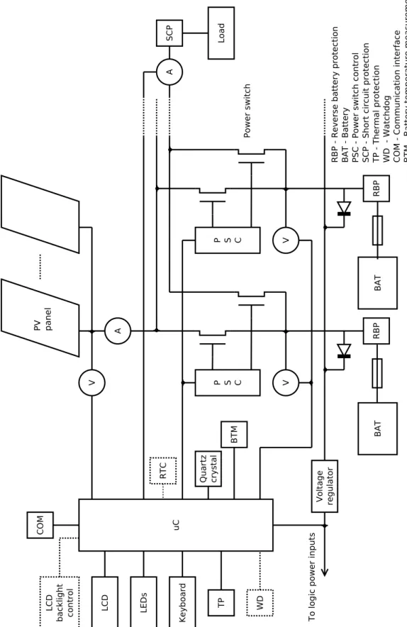
Based on the intended functionality mentioned in the previous chapter, the prelimi-nary block diagram of the charge controller in Fig.1.2 has been devised.
1.3.1
Preliminary Block Diagram
The exact number of batteries is not indicated in the Fig.1.2, as it is not defined yet. It will be determined according to hardware design possibilities that will be clearer at a later stage. It will mostly depend on the added cost and complexity of hardware and the design will aim to make this number as high as is practical.
The regulator built according to this block diagram will have capability to mea-sure the voltages of all batteries. These meamea-surements can be used by the microcon-troller (µC) to control the inputs from solar panel to each battery separately and the outputs to load in the same way. So the controller will have possibility to stop
charging, when the battery is fully charged as well as disconnect the load, when it is fully discharged.
The diagram contains also some optional blocks that may not be implemented in final version. However, these have been included in order to show the configuration of blocks if all of the desired functionality is implemented.
1.3.2
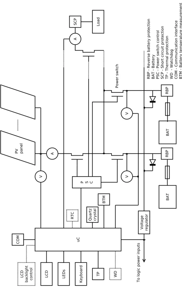
Updated Block Diagram
The block diagram in Fig. 1.2 has been used throughout most of the design phase, because the switches were assumed to be unidirectional. However, later it was dis-covered that it can be simplified.
The simplification is based upon using only one common path for currents from solar panel to batteries and from batteries to load, as shown in Fig. 1.3. This was possible after a specific design of power switches done in Section 2.1.1 was changed so that the switches were made bidirectional.
In order to ensure that the regulator can perform charging correctly, two more switches had to be added. Namely a switch that can disconnect a solar panel and a switch to disconnect load, when all of the batteries on the common bus are fully charged or discharged. The regulator will of course be able to choose which battery will be connected to the bus. This way all the major objectives can be fulfilled.
For more details about the design of power switches, reasons for making the change and the details about the simplification please refer to Section 2.1.1.
The preliminary block diagram has set a basic shape for the controller design that could lead to fulfilment of highest level requirements as well as created logical sub-blocks. For these blocks, separate detailed requirements can be made.
1.4
Definition of Design Requirements for Building
Blocks
The elements of the block diagrams from the previous section should ideally have following characteristics:
LCD – for displaying information about battery and controller state and measured
data. The display may need to be switched on only for short periods of time after any key is pressed due to power saving reasons.
LEDs – two low power consumption LEDs (red and green) for indication of correct
PV panel V A V RB P Rev er se ba tte ry protection B AT B atte ry PSC Pow er s w itch control SCP Short cir cuit pr ot ection TP Th erma l prot ec tion W D - Wa tch d og C O M C o mm unica tio n interface B TM B attery t em p e ra ture meas uremen t RBP BAT P S C V RBP BAT P S C A SCP Load TP WD Voltage regulator LCD K eyb oa rd uC To log ic p ower input s Power switch LCD
backlight control LEDs
COM
Quartz crystal
BTM
RTC
PV panel V A V RB P Rev er se ba tte ry protection B AT B atte ry PSC Pow er s w itch control SCP Short cir cuit pr ot ection TP Th erma l prot ec tion W D - Wa tch d og C O M C o mm unica tio n interface B TM B attery t em p e ra ture meas uremen t RBP BAT V RBP BAT P S C A SCP Load TP WD Voltage regulator LCD K eyb oa rd uC To log ic p ower input s Power switch LCD
backlight control LEDs
COM
Quartz crystal
BTM
RTC
Keyboard – for controlling regulators’ functionality and setting parameters. Only
three keys (up, down and enter) should be needed, if sophisticated menu is
implemented.
Thermal protection – a temperature sensor capable of measuring temperatures
in the range from -30 to about +160∘C.
Battery temperature measurement – a temperature sensor capable of
measu-ring temperatures in the range from -30 to about +50∘C.
External watchdog (optional) – should restart a µC after specified time interval
(between 150 and 1200ms) and after a power failure.
Voltage regulator – will have to be chosen according to sum of maximum
con-sumption of active components such as µC that it will feed power to.
Reverse battery protection – has to be able to withstand voltage of about 30V
and prevent damage of controller and/or batteries.
Short circuit protection – should disconnect the load when it is shorted. Its
pa-rameters depend on the kind of switches used, as this is mainly for their pro-tection. It also has to have least possible series resistance.
Power switch control – should convert voltages that will be an output of the µC
to levels that are large enough for power switches used.
Battery – a lead-acid battery with nominal voltage of 12V.
Serial communication interface – to be able to communicate with a PC or to
decompose the regulator into more parts (e.g. main part and a user interface module and/or datalogging module).
Voltmeter by the PV panel – should be able to withstand voltages in range of 0
to +25V (as the PV panel nominal voltage of 12V generates about 24V when load is disconnected).
Voltmeters by the batteries – should work in range of 0 to +15V.
Ammeter – the measuring range should be 0 to little over 20A to be able to detect
over-current condition.
Power switch – should be able to handle currents of 20A or higher (ideally at least
30A so that there is some reserve) and withstand voltages of 30V or higher. Very low series resistance is also a must.
LCD backlight control – should be able to switch the currents needed by
backli-ght of the LCD module according to a logic signal on one pin of the µC. The backlight should ideally be switched off after about 15s from pressing one of the keys last time in order to decrease the overall power consumption of the device.
Quartz crystal resonator – for the internal clock signal generator of µC. Its
va-lue should be considered according to computational power requirements of algorithms used and the power consumption of the µC. Currently 2MHz value
is considered to be a good compromise.
Microcontroller – needed as most of the planned functionality of charge
cont-roller requires use of digital electronics for implementation. The µC should have enough pins for at least the mandatory features (if µC with fewer pins is selected, some of the optional functionality may not be implemented). As the exact memory requirement will not probably be known until most of the algorithms are actually developed, µC with more built in memory should be preferred (even if not used by algorithms, it can be utilized for logging pur-poses). The µC may have internal Analog to Digital Converter (ADC) to save an extra part, but in this case must have enough inputs for it.
Real-Time Clock (optional) – using it for timekeeping instead of counting the
time in the microcontrollers main loop will allow the µC to sleep when no other tasks need to be calculated, thus saving power.
When the design requirements for all of the individual building blocks have been specified, it is possible to carry out the design by these requirements itself, as is done in the following chapter.
2
HARDWARE DESIGN
This chapter concentrates on all aspects of hardware (HW) design of the controller, such as the realization of individual building blocks, issues connected to intercon-nection of these blocks, producing the Printed Circuit Board (PCB) and prototype of the regulator.
2.1
Design of Fundamental Building Blocks
There are three stages of designing this block that have been labelled as the first design, second design and the third (and final) design. After encountering problems that will be specified later, the original conceptual solution (first design) has been redesigned. Later was found that the second design can be substantially simplified with little or no effect on functionality.
The biggest difference between the first two designs is that the first design relied on using the positive terminals of the batteries as 0V and was supposed to work with negative voltages. This idea has been abandoned later and the second design uses the minus pole as a common reference and works with positive voltages. The reason for this change will be explained in detail in paragraph Second design (Section 2.1.1).
The siplifications that lead to the third design deal mainly with the power swit-ching and do not impact other building blocks very much. More details will be discussed in paragraph Third design (Section 2.1.1).
2.1.1
Power Switch and Power Switch Control
As the power switches are probably the most important parts of the proposed regu-lator, their design is considered first. Their significance is due to fact there are more of them and also because they have the biggest impact on the final performance.
Switching Technology Selection
Following technologies have been considered as a possible building block for indivi-dual switching element:
• relay,
• Solid State Relay (SSR), • bipolar transistor, and
• Metal-Oxide-Semiconductor Field-Effect Transistor (MOSFET).
The relays have an advantage that they behave like an ideal switch – infinite resistance in open position and very little resistance in closed state. Among the disadvantages are their size and the fact that they are electromechanical devices
so they may be more prone to failure after some time. They are also quite slow compared to bipolar and unipolar transistors, so they can hardly be used for Pulse-Width Modulation (PWM).
Solid State Relays have fewer disadvantages than usual relays thanks to no me-chanical components, but they are not suitable for DC switching application. The commercially available SSRs suitable for high enough currents actually contain tri-acs. Besides this, the devices that can handle 20A or more continuously cost about 11 times more than MOSFET transistors for comparable currents.
Bipolar transistors have an obvious disadvantage of a voltage drop equivalent to a diode drop (so about 0.6V) on them even if closed. This would result in huge power losses if currents as high as proposed nominal current of 20A flew through them. In such case the transistor would dissipate 12W of power (in reality even more, because the voltage drop over the transistor would be bigger with current of 20A, which is the highest nominal current that this regulator will be designed for).
The MOSFETs are currently capable of switching more than one hundred Ampe-res continuously (for example transistor IRFP064N made by International Rectifier can withstand 110A continuously with proper cooling) have a static drain-to-source
on-resistance (RDS(on)) as low as 5mΩ. What is more, the prices are competitive with
any of the above-mentioned technologies. They come in two flavors: N-channel and P-channel. The N-channel transistors usually have better performance
characteris-tics (lower RDS(on), able to switch higher currents) and lower price than P-channel
transistors. However, they have one big disadvantage: The only simple way of con-necting them in the circuit requires that the terminal that is switched is negative.
Fig. 2.1: An example of a using MOSFET as a switch [9]
The situation and the reason for this can be illustrated on diagram in Fig. 2.1. The MOSFET is turned on by a positive voltage applied between Gate and Source
terminals. This voltage can be taken directly from VDD if it is less than 20V,
otherwise the voltage divider has to be used. Note that the Source is placed at 0V in this case, so the voltage to turn on the transistor can be related to 0V. If the
transistor was placed between the VDD and lamp, the voltage to turn the transistor
on would have to be applied between Gate and Source terminal and it would have
to be more positive than VDD. Another problem is that the Source would not have
a defined potential, because that depends on the current flowing through the lamp. That is why N-channel MOSFETs are usually used in circuits such as in Fig. 2.1.
After considering all these facts, N-channel MOSFETs have been chosen as the most suitable switching technology. The reason is mainly that using this technology PWM switching will be possible if needed and the power losses can be kept as low as possible.
But this decision comes at a cost of adding complexity to the design. As was already mentioned, there is a problem with switching the positive poles with the N-channel MOSFET switches. To overcome this problem, the two approaches can be used:
1. connecting MOSFETs so that they disconnect negative poles of batteries. As a result the positive terminals will have to be used as common poles (or 0V) instead of negative terminals, as is normal under usual conditions. The negative voltages will have to be used, which means more complicated design of voltage regulation for logic and more complicated voltage measurement, as ADCs work with positive voltages only. This approach was used in the first design that will be described in the next chapter.
2. placing MOSFETs in the positive branches (and using negative poles of bat-teries as a common terminal) and generating a higher voltage for the
gate-to-source voltage (VGS) than the voltage to be switched. This will require some
switching power supply or charge pump that could create higher voltage than the 12V nominal voltage that is already present in the system. There will also be problems with the gate potential floating. However, designing other subsystems (e.g. current measurement, ADC, etc.) will be easier due to ha-ving negative pole as a ground. This was later used in the Second design (Section 2.1.1).
After a preliminary selection a concrete type of MOSFET transistor has been selected: IRF3205 produced by International Rectifier. This transistor can handle
drain-to-source voltage (VDSS) up to 55V, continuous drain current (ID) of 110A,
its RDS(on) is equal to 8.0mΩ and it comes in TO220A package [17]. It is readily
available in retail stores for prices of about 0.8 Euro.
This transistor clearly suffices our maximum current requirement and has also
However, if the price of MOSFETs with better quality drops to an adequate le-vel, it can easily be replaced as most power MOSFETs are produced in TO220A package as well.
First Circuit Design
This is the design, where the positive terminals are used as common poles.
In the very beginning, there was only one transistor planned in one branch to be switched. After a test on the real circuit it is clear, that such design is not satisfactory. The reason is the MOSFET’s body diode in the reverse direction. With this diode, the MOSFET can be used as a unidirectional switch only. If the voltage is applied in the reverse direction, the transistor conducts current as soon as the voltage reaches threshold level for diode conduction (about 0.6V).
The problem is that for successful isolation of the batteries from each other a bidirectional switch is needed (the current can not flow in any direction when the switch is open). Two solutions for this situation have been thought of:
• using a diode in series of the MOSFET, and • using another MOSFET in opposite direction.
If the diode was used, the power losses would increase dramatically, since power would be lost due to a relatively high voltage drop on the diode. On the contrary, with using another MOSFET, the power loss would be smaller, because of the low
RDS(on)value of MOSFETs used. At currents equal to 20A MOSFET would dissipate
power equal to
𝑃MOSFET=𝑉 ·𝐼 =RDS(on)·𝐼2 = 0.008·202 = 3.2W (2.1)
whereas diode would dissipate
𝑃diode=𝑉 ·𝐼 = 0.6·202 = 12W (2.2)
Of course the less power hungry solution was selected, even though it is still not ideal, because the power losses on the switch will be effectively doubled.
When used in practice, the second MOSFET has to be switched on together with the first one. Otherwise the current would flow through the body diode. That would result in the same heat dissipation as calculated in formula 2.2.
The bidirectional design of the power switch can be seen in Fig. 2.2. Note that the displayed types of transistors Q1, Q2, Q5 and Q6 are not correct and should be IRF3205. In this case it makes no difference, since the symbol and package of the two types of transistors are the same.
Fig. 2.2: Scheme of power switches for one battery
Theory of Operation The transistors Q1 and Q2 in Fig. 2.2 make up a pair that
connects or disconnects the supply from the PV panel to battery (BAT1). As they are turned on by positive voltage applied between their Drain and Source terminals the transistors Q3 and Q4 with the resistors R3 and R4 have to be used.
The source of the Q2 is connected to –UBAT1, which means the transistor is open when its gate is at potential of –UBAT1 (or lower) and closed when the gate is at potential of –UBAT+5V or higher (up to –UBAT+20V). The Q4 with R4 actually convert the voltage levels of 0 and -5 volts from microcontroller applied to SWITCH_1A wire into either –UBAT or almost 0V (this was inspired by an example in [1]). Transistor Q4 is a P-channel MOSFET, so in this position (when source is at 0V) is turned on by -5V. When Q4 is off, there is no current flowing through R4, so the voltage between Q2’s gate and source is 0V and Q2 is closed. On the other hand, if Q4 is open, there is a voltage of almost UBAT on the R4 due to current flowing which in turn turns on Q2.
The same logic applies in case of Q1 and Q3. The only difference is that there is a Zener diode D2 and a resistor R9 added. They serve as a protection against overvoltage from PV panel that could happen because PV panel for nominal voltage of 12V can generate up to 25V when no load is connected. The MOSFETs can
protection can be applied directly at the input from PV panel. That way the D2 and R9 and their counterparts in switching circuitry for other batteries can be omitted. Q5 and Q6 switch the output from the battery to load according to logic sig-nal from µC applied at SWITCH_1B. The VOLTAGE_REGULATOR_IN output feeds should be connected to voltage regulator that will power the microcontroller and other logic.
In this configuration the block in Fig. 2.2 can be used for any number of bat-teries and the VOLTAGE_REGULATOR_IN, PV_PANEL and LOAD wires out-puts can be connected in parallel. This way only logic levels on SWITCH_nA or SWITCH_nB inputs will decide which battery is connected to solar panel and/or to load.
Drawbacks The biggest problem with this approach lies in voltage and current
measurement. Mainly it is the issue of powering the ADC and what potential to use as a ground potential.
The ADC could be connected with its VCC terminal directly to 0V and -5V could be generated by 7905 circuit, which references its output to positive terminal. The problem is that the ground for ADC generated this way changes a little, because the load regulation on 7905 circuit can’t be perfect. This would add another error to measurement, as all the measured voltages will be referenced to 0V and not to -5V.
This problem could be eliminated by using the 0V as a ground for ADC and powering it by +5V generated by some external circuit. This solution requires a more complicated component (power source), but does not solve the problem with grounds in current measurement, for which a specialized circuit will be used (current measurement will be discussed in subsequent chapter).
As a workaround for the abovementioned issues in this first design could not be found, a second design has been proposed.
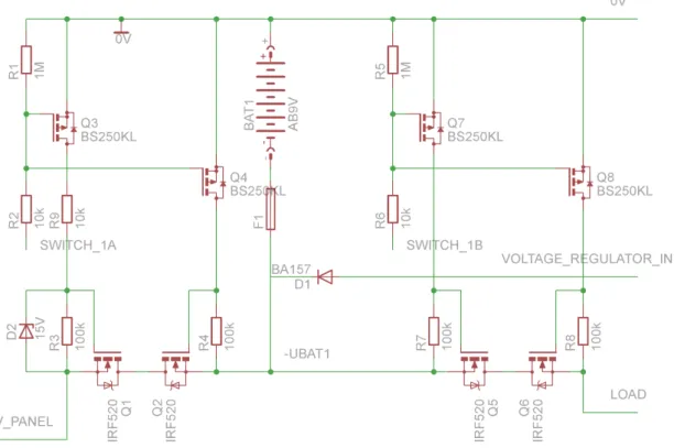
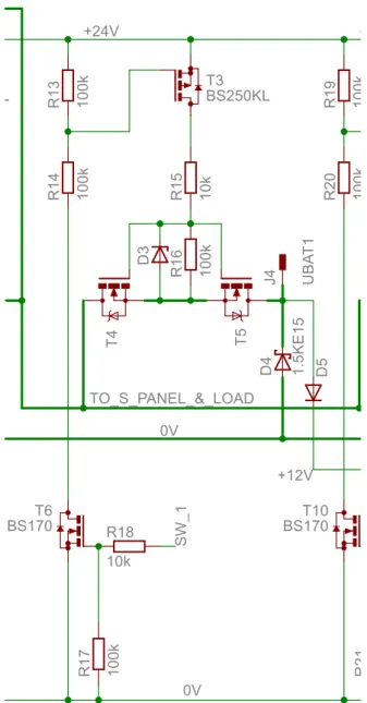
Second Design
As was already mentioned, in this design the negative terminals of all batteries will be connected and this will be treated as 0V. The plus poles of the batteries will be switched. This can be seen on a schematic of a switching circuit for one battery in Fig. 2.3.
The plus pole of the battery will be connected to board via connector labeled as J4. The connector for the negative pole is not drawn in the picture, but it will be connected to 0V elsewhere.
2 1 . 1 2 . 2 0 1 0 1 6 :4 3 :5 2 C :\U se rs\ P e te r_ 2 \D o cu m e n ts\ e a g le \d ip l_ 0 3 \p o w _ b o a rd _ 4 0 .sch ( S h e e t: 1 /1 ) BS170 1 0 0 k 10k 2 k 1 .5 K E 1 5 1 0 k BS170 1 0 0 k 10k 2 k 1 .5 K E 1 5 1 0 k 1 0 0 k 1 0 k BS250KL 1 0 0 k 1 0 0 k 1 .5 K E 1 5 BS170 1 0 0 k 10k 2 k 1 0 0 k 1 0 k BS250KL 1 0 0 k 1 0 0 k BS170 1 0 0 k 10k 2 k 1 0 0 k 1 0 k BS250KL 1 0 0 k 1 0 0 k 1 .5 K E 1 5 BS170 1 0 0 k 10k 2 k 1 0 0 k 1 0 k BS250KL 1 0 0 k 1 0 0 k BS170 1 0 0 k 10k 2 k ICL7662CPA 9 k 1 4 k 7 L M 3 3 5 IF B 2 O U T 5 V C C 3 IN 1 T1 R 4 R5 R 6 R 1 R 2 C3 J1 J2 D 1 C1 C2 R 3 IF B 2 O U T 5 V C C 3 IN 1 T2 R 7 R8 R 9 R 1 0 R 1 1 C4 D 2 C5 C6 R 1 2 J3 T 4 T 5 D 3 R 1 6 R 1 5 T3 R 1 3 R 1 4 J 4 D 4 D 5 T6 R 1 7 R18 R 1 9 T 7 T 8 D 6 R 2 0 R 2 1 T9 R 2 2 R 2 3 T10 R 2 4 R25 R 2 6 T 1 1 T 1 2 D 7 R 2 7 R 2 8 T13 R 2 9 R 3 0 J 5 D 8 D 9 T14 R 3 1 R32 R 3 3 T 1 5 T 1 6 D 1 0 R 3 4 R 3 5 T17 R 3 6 R 3 7 T18 R 3 8 R39 R 4 0 TEST 1 GROUND 3 CAP- 4 V+ 8 VOUT 5 LV 6 OSC 7 CAP+ 2 IC3 D11 D12 C7 C8 R 4 1 1 2 3 4 5 6 7 8 9 10 11 12 13 14 15 16 CON1 F1 F2 F3 R 4 2 IC 4 R 4 3 A E S R 4 5 L E D 8 L E D 7 L E D 6 L E D 5 L E D 1 L E D 2 L E D 3 L E D 4 J6 CON2-1 CON2-2 CON2-3 CON2-4 CON2-5 CON2-6 CON2-7 CON2-8 TO_LOAD T O _ L O A D TO_LOAD LOAD S W _ 1 SW_1 0V 0V 0V 0V 0V 0V 0V S_PANEL S_PANEL S W _ 2 SW_2 UBAT2 U B A T 2 +24V +24V + 2 4 V +24V +12V +12V +12V S W _ 3 SW_3 S W _ 4 SW_4 UBAT1 U B A T 1 S W _ 5 SW_5 S W _ 6 SW_6 TEMP_SENSE T E M P _ S E N S E TO_S_PANEL CUR_SENSE_2 C U R _ S E N S E _ 2 CUR_SENSE_1 C U R _ S E N S E _ 1 IC1 + IC2 + + +
Fig. 2.3: The schematic of a power switch for one battery – second design There are again two MOSFETs in each switched branch (to solar panel and to load). However, another improvement against first design is that the source terminals of both transistors are connected together, instead of drain terminals. This allows
one driving voltage to be applied to both transistors as VGS. This voltage is created
on R16 and R20 when transistors T3 and T9 are turned on.
In order to create positive VGS, the transistors T3 and T9 have to switch more
positive voltage than what UBAT1 is. The reason is that the sources of the power transistors now sit on a potential UBAT1+0.7 which is the voltage drop created on the body diode of T5 for example.
As the power transistors are fully open at VGS of about 10V and the maximum battery voltage when charging should be about 14.1V, the source of about +24V
has been chosen for powering the auxiliary transistors T3 and T9. The way +24V is generated is described in Section 2.2.3.
Several elements had to be added for the protection of the power MOSFETs, namely resistors R15, R21 and Zener diodes D3 and D6 in the Fig. 2.3. The reason
is that the transistors could get damaged by excessive VGS. The absolute maximum
value the transistors can withstand is ±20𝑉. This threshold could be exceeded if
there was no battery connected to J4 and the load was connected to the output of the regulator. In this situation the load would in fact connect the TO_LOAD line to 0V. In this case the sources of T7 and T8 would sit on the potential of 0.7V. If
the T9 was opened in this situation, the VGS would be almost +24V. The situation
gets worse as the voltage on the +24V line can reach +27V. This overvoltage would definitely lead to destruction of the power transistors.
Although it seems that the protection is required only on a switch between battery and load, it is not true. The same thing could happen to transistors T4 and T5 if the switch to load would be closed in the previous situation.
The risk of damaging the power MOSFETs can be avoided by using Zener diodes D3 and D6 with a Zener voltage lower than +20V limit under the highest load condition on these diodes. In order to limit the current through them, the resistors R15 and R21 are used.
For this application the current limiting resistors R15 and R21 with nominal value 10k and diodes with Zener voltage equal to 16V have been chosen. The resistors should limit the current at worst conditions to:
Imax = V
+24Vmax−VZener
R =
27−16
104 = 1.1mA (2.3)
This current is low enough not to cause thermal problems with diode or resis-tor and low enough for the dynamic resistance of Zener diodes to have no impact on functionality of the protection (the Zener voltage of the diode selected loaded with 5mA should be in the range of 15.3-17.1V which is well below the dangerous
threshold for VGS).
Finally the transistors T6 and T10 together with resistors R13, R14, R22, R23 are used for the translation of the driving voltage from logic (0-5V) to appropriate levels for T3 and T9.
The rest of the parts are used because of integration of a power switch for single battery to the whole system and the details will be discussed in Section 2.2.2.
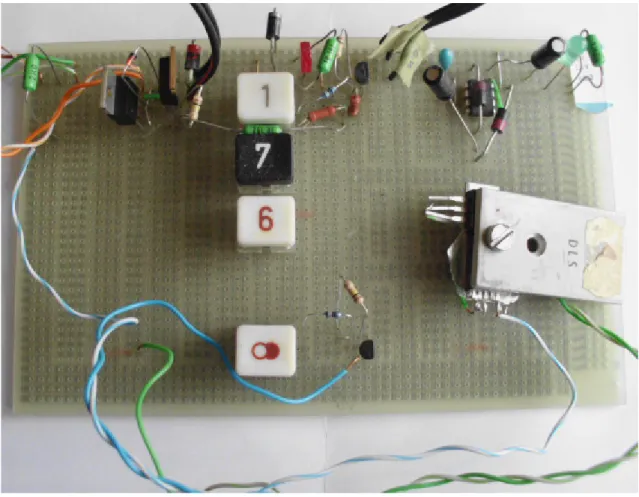
In order to verify the functionality of this switch a temporary test circuit on development board has been prepared and the correct performance was verified. The picture in Fig. 2.4 shows switch for switching one branch (from battery to load) for one battery (top, from left to center), the source of +24V (top right) and the current
measurement circuit (on an aluminium heat sink), whose correct functionality was also verified.
Fig. 2.4: Test implementation of second design of power switch
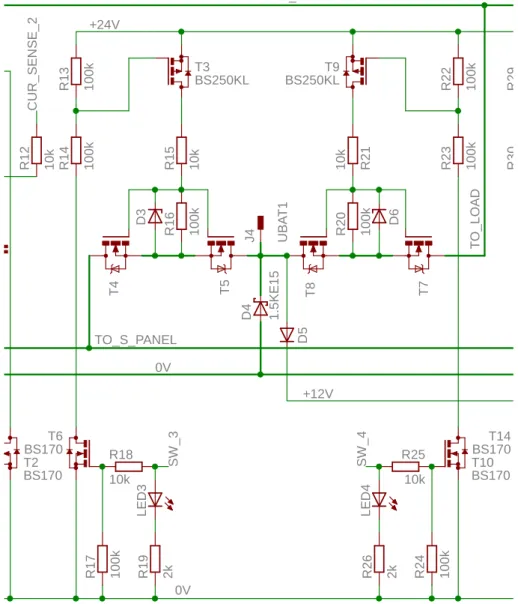
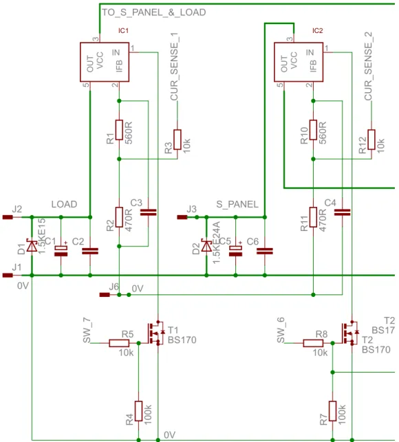
Third Design
As was already mentioned, the third design is a simplification of the second design. It is based on fact that the path connecting a battery with solar panel and a path connecting a battery with load do not have to be separate and can be combined into one, as was shown in block diagram 1.3.
Its schematic is shown in Fig. 2.5. When compared with the schematic of the previous design in Fig. 2.3, it can be seen that it was created by simply omitting the right half, that was connecting the battery to load. The power line that used to be called TO_S_PANEL has become TO_S_PANEL_&_LOAD. It is clear that the biggest changes have been made on a system level.
This systematic solution seems to have a potential disadvantage, that it is not possible to control whether the connected battery is going to be charged or dischar-ged, as it depends on the instantaneous power fed by solar panel and used by load.
BS170 1 0 0 k 10k 1 .5 K E 1 5 1 0 k BS170 1 0 0 k 10k 1 .5 K E 2 4 A 1 0 k 1 0 0 k 1 0 k BS250KL 1 0 0 k 1 0 0 k 1 .5 K E 1 5 BS170 1 0 0 k 10k ICL7662CPA 9 k 1 L M 3 3 5 1 0 0 k 1 0 k BS250KL 1 0 0 k 1 0 0 k 1 .5 K E 1 5 BS170 1 0 0 k 10k 1 0 0 k 1 0 k BS250KL 1 0 0 k 1 0 0 k 1 .5 K E 1 5 BS170 1 0 0 k 10k 1 0 0 k 1 0 k BS250KL 1 0 0 k 1 0 0 k 1 .5 K E 1 5 BS170 1 0 0 k 10k 1 0 0 k 1 0 k BS250KL 1 0 0 k 1 0 0 k 1 .5 K E 1 5 BS170 1 0 0 k 10k CON2 1 0 0 k 1 0 k BS250KL 1 0 0 k 1 0 0 k BS170 IF B 2 O U T 5 V C C 3 IN 1 T1 R 4 R5 R 1 R 2 C3 J1 J2 D 1 C1 C2 R 3 IF B 2 O U T 5 V C C 3 IN 1 T2 R 7 R8 R 1 0 R 1 1 C4 D 2 C5 C6 R 1 2 J3 T 4 T5 D 3 R 1 6 R 1 5 T3 R 1 3 R 1 4 J 4 D 4 D 5 T6 R 1 7 R18 TEST 1 GROUND 3 CAP- 4 V+ 8 VOUT 5 LV 6 OSC 7 CAP+ 2 IC3 D11 D12 C7 C8 R 4 1 1 2 3 4 5 6 7 8 9 10 11 12 13 14 15 16 CON1 F1 F2 F3 IC 4 R 4 3 A E S R 4 5 L E D 1 J6 T 7 T8 D 6 R 6 R 9 T9 R 1 9 R 2 0 J 5 D 7 D 8 T10 R 2 1 R22 T 1 1 T 1 2 D 9 R 2 3 R 2 4 T13 R 2 5 R 2 6 J 7 D 1 0 D 1 3 T14 R 2 7 R28 T 1 5 T 1 6 D 1 4 R 2 9 R 3 0 T17 R 3 1 R 3 2 J 8 D 1 5 D 1 6 T18 R 3 3 R34 T 1 9 T 2 0 D 1 7 R 3 5 R 3 6 T21 R 3 7 R 3 8 J 9 D 1 8 D 1 9 T22 R 3 9 R40 CON2-1 CON2-2 CON2-3 CON2-4 CON2-5 CON2-6 CON2-7 CON2-8 CON2-9 1 J P 1 2 T 2 4 D 2 0 R 4 2 R 4 4 T25 R 4 6 R 4 7 T26 LOAD SW_1 S W _ 1 0V 0V 0V 0V 0V 0V 0V 0V 0V 0V 0V 0V 0V 0V 0V S_PANEL S_PANEL SW_2 S W _ 2 U B A T 2 UBAT2 +24V + 2 4 V +24V +24V +24V +24V +24V +12V +12V +12V +12V +12V +12V SW_3 S W _ 3 SW_4 S W _ 4 U B A T 1 UBAT1 SW_5 S W _ 5 SW_6 S W _ 6 T E M P _ S E N S E
TO_S_PANEL_&_LOAD TO_S_PANEL_&_LOAD TO_S_PANEL_&_LOAD TO_S_PANEL_&_LOAD TO_S_PANEL_&_LOAD
TO_S_PANEL_&_LOAD CUR_SENSE_2 C U R _ S E N S E _ 2 CUR_SENSE_1 C U R _ S E N S E _ 1 U B A T 3 UBAT3 U B A T 4 UBAT4 U B A T 5 UBAT5 SW_7 S W _ 7 IC1 + IC2 + + +
Fig. 2.5: The schematic of a power switch for one battery – third design Both of these will change independently of each other. But thanks to the measu-rement of current from solar panel and to load the measured difference in current can be used to determine if we are charging or discharging the battery. So if the control algorithm decides some specific battery needs to be charged and a different one discharged, it can switch between them according to results of current measu-rement. This shows that this design can be used without the loss of generality for the control algorithm, provided that the currents from solar panel and to load are measured.
On the other hand, this solution has several advantages:
• There are fewer high current paths, which will simplify the design of PCB and make more space so that the paths can be made wider.
• There will be smaller losses than if there were two paths – if there is both current from panel and to load, part of the current will flow directly to load, thus decreasing losses thanks to shorter path.
• Fewer parts are needed – the regulator can be made smaller or it may be possible to control more batteries on the same area of the board.
• Fewer microcontroller pins are needed for more batteries – only one switch for one battery plus two switches for controlling solar panel and load, opposed to two switches per battery.
2.1.2
Current Measurement
The need for the measurement of current from solar panel to batteries and from batteries to load originates in the requirement for power measurements. It should be implemented also if the regulator worked according to the design described by updated block diagram (Fig. 1.3). The current flowing to the load can be used for detecting over-current conditions as well.
Principle and Selection of Implementation Method
Firstly we must define what properties of the current measurement circuit are of the biggest concern. These are:
• precision (the more precise the better), • range (0-20A nominal),
• low voltage drop on measurement device, and • price.
As the current to be measured is DC, there is a limited amount of proven solutions available. The following main methods have been considered:
• measuring a voltage drop on a shunt resistor, and • using specialized measurement ICs.
The first method is simple and may be very precise, but there are several disa-dvantages in our application. Due to big range of current to be measured the shunt resistor would have to be very small. Even with the shunt resistor with resistance as
low as 10mΩ there would be considerable power dissipation on it if highest nominal
current flew through it:
Pmax=R·Imax= 0.01·202 = 4W (2.4)
This heat dissipation would pose big problems with the change of the resistance of material because of temperature coefficient. Moreover, it would increase the overall consumption of the device.
Another disadvantage is that the voltage drop on such shunt would have to be amplified, which would increase the complexity of the design.
It is also possible to measure the voltage drop on a MOSFET switch or a PCB track (as is described in [10]), but these modifications suffer from the same problems as using the shunt resistor in this design. Moreover the voltage drop on MOSFET is very dependent on temperature.
There are specialized current measurement integrated circuits on the market nowadays. Most of them are in fact Hall effect sensors with integrated signal condi-tioning circuitry. These are the products that were considered more closely:
• Hall Effect-Based Linear Current Sensor ICs from Allegro microsystems – the
ACS75x family [11]. These sensors feature very small resistance (100µΩ) and
typically less than 4% total error from -40∘C to 150∘C. The devices from this
family were considered, but there was a problem with the availability of the part at a time of decision which technology to use.
• Small sized current sensor CQ-121E from company Asahi Kasei Microdevices Corporation (AKEMD) [12]. This part has not been considered either because of the same reason – no retailer for this part has been found.
• Inductive Analog Current Sensors from Honeywell, such as (CSLA2CD or CSNE151). These sensors are available, but they consume considerable amount of power (CSLA2CD – 20mA [13], CSNE151 – 10mA [14]) and are quite costly (about 15 Euros per one piece in Dec. 2010).
• Programmable current sense high side switch IR3313 from International
Recti-fier. This IC features 7mΩ on resistance, 2% error if calibrated, short circuit
protection and thermal protection for the price of about 5 Euros per piece. Its datasheet can be found in [15].
The IR3313 device has been chosen for this application, because the output signal does not need to be amplified (no added complexity), it is available in online stores and the built in short circuit protection feature will further simplify the design of the regulator (it will eliminate the need for separate module to achieve this goal).
Implementation
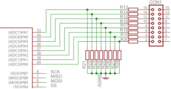
The basic circuit connection of the IR3313 devices can be seen in Fig. 2.6. The explanation below will concentrate only on one of the circuits shown (namely IC1), as the important characteristics are equivalent also for IC2.
Intelligent switch is controlled by the voltage difference between VCC and IN pin. If T1 is turned on, the voltage difference between the two pins is higher than the specified threshold and IC1 turns on as well. A current proportional to the current through the integrated power MOSFET is sourced to the IFB pin (current
BS170 1 0 0 k 10k 5 6 0 R 4 7 0 R 1 .5 K E 1 5 1 0 k BS170 1 0 0 k 10k 5 6 0 R 4 7 0 R 1 .5 K E 2 4 A 1 0 k 1 0 0 k 1 0 k BS250KL 1 0 0 k 1 0 0 k 1 .5 K E 1 5 BS170 1 0 0 k 10k ICL7662CPA 9 k 1 L M 3 3 5 1 0 0 k 1 0 k BS250KL 1 0 0 k 1 0 0 k 1 .5 K E 1 5 BS170 1 0 0 k 10k 1 0 0 k 1 0 k BS250KL 1 0 0 k 1 0 0 k 1 .5 K E 1 5 BS170 1 0 0 k 10k 1 0 0 k 1 0 k BS250KL 1 0 0 k 1 0 0 k 1 .5 K E 1 5 BS170 1 0 0 k 10k 1 0 0 k 1 0 k BS250KL 1 0 0 k 1 0 0 k 1 .5 K E 1 5 BS170 1 0 0 k 10k CON2 1 0 0 k 1 0 k BS250KL 1 0 0 k 1 0 0 k BS170 IF B 2 O U T 5 V C C 3 IN 1 T1 R 4 R5 R 1 R 2 C3 J1 J2 D 1 C1 C2 R 3 IF B 2 O U T 5 V C C 3 IN 1 T2 R 7 R8 R 1 0 R 1 1 C4 D 2 C5 C6 R 1 2 J3 T 4 T5 D 3 R 1 6 R 1 5 T3 R 1 3 R 1 4 J 4 D 4 D 5 T6 R 1 7 R18 TEST 1 GROUND 3 CAP- 4 V+ 8 VOUT 5 LV 6 OSC 7 CAP+ 2 IC3 D11 D12 C7 C8 R 4 1 1 2 3 4 5 6 7 8 9 10 11 12 13 14 15 16 CON1 F1 F2 F3 IC 4 R 4 3 A E S R 4 5 L E D 1 J6 T 7 T8 D 6 R 6 R 9 T9 R 1 9 R 2 0 J 5 D 7 D 8 T10 R 2 1 R22 T 1 1 T 1 2 D 9 R 2 3 R 2 4 T13 R 2 5 R 2 6 J 7 D 1 0 D 1 3 T14 R 2 7 R28 T 1 5 T 1 6 D 1 4 R 2 9 R 3 0 T17 R 3 1 R 3 2 J 8 D 1 5 D 1 6 T18 R 3 3 R34 T 1 9 T 2 0 D 1 7 R 3 5 R 3 6 T21 R 3 7 R 3 8 J 9 D 1 8 D 1 9 T22 R 3 9 R40 CON2-1 CON2-2 CON2-3 CON2-4 CON2-5 CON2-6 CON2-7 CON2-8 CON2-9 1 J P 1 2 T 2 4 D 2 0 R 4 2 R 4 4 T25 R 4 6 R 4 7 T26 LOAD SW_1 S W _ 1 0V 0V 0V 0V 0V 0V 0V 0V 0V 0V 0V 0V 0V 0V 0V S_PANEL S_PANEL SW_2 S W _ 2 U B A T 2 UBAT2 +24V + 2 4 V +24V +24V +24V +24V +24V +12V +12V +12V +12V +12V +12V SW_3 S W _ 3 SW_4 S W _ 4 U B A T 1 UBAT1 SW_5 S W _ 5 SW_6 S W _ 6 T E M P _ S E N S E
TO_S_PANEL_&_LOAD TO_S_PANEL_&_LOAD TO_S_PANEL_&_LOAD TO_S_PANEL_&_LOAD TO_S_PANEL_&_LOAD
TO_S_PANEL_&_LOAD CUR_SENSE_2 C U R _ S E N S E _ 2 CUR_SENSE_1 C U R _ S E N S E _ 1 U B A T 3 UBAT3 U B A T 4 UBAT4 U B A T 5 UBAT5 SW_7 S W _ 7 IC1 + IC2 + + +
Fig. 2.6: The connection of IR3313 current measurement ICs in the circuit feedback). If the voltage between IN and IFB pin is higher than about 4.7V, the over current condition is detected and the switch is turned off [15]. The current shutdown threshold is adjusted by selecting the proper resistor between IFB and ground.
The implementation devised for this application uses similar structure as is re-commended in the datasheet (the feedback resistor R2, resistor R3 and transistor T1 for turning the IC1 on). The schematic includes also capacitor C3 in case there was excessive noise that would have to be eliminated. This part will be soldered into PCB only if it is needed.
Resistor R1 together with R2 form a voltage divider that can be used to decrease the voltage going to measurement circuit and therefore eliminate the need for divider at the input of ADC.
The values of R1 and R2 are chosen according to several criteria. One of them is to set the over current shutdown threshold to a specific value. This value depends on a sum of resistances of R1 and R2 and should be higher than the nominal vol-tage, because of the inrush currents when using certain loads (e.g. filament lamps). According to application note for IR3313 [16], the inrush current can be as high as 7 times the nominal current. Therefore the threshold should be higher than the designed nominal current of 20A.
As there is a low chance that there will be filament lamps of high wattages used, we suppose there will be more lamps with lower wattages. By using our judgment we estimate that setting the current threshold to about the double of nominal current should be sufficient. If the practical experience shows later this value is underesti-mated, the value of R1 and R2 can be changed later if needed.
As was already mentioned, the 4.7V threshold of IR3313 over-current shutdown should represent about 40A, so the desired value of resistors in feedback branch can be calculated: R1+R2 = V threshold Imax Ratio = 440.7 8800 = 1034Ω, (2.5)
where Ratio is the ratio between the current through the power MOSFET of IR3313 and the current sourced to IFB pin provided by datasheet [15].
Note that setting the over current threshold on IR3313 power switch to value higher than the nominal value for the regulator does not decrease the safety of the device, as the over current conditions lasting longer can be detected by program in microcontroller based on reading from the current measurement circuitry and the load will be disconnected if the condition lasts more than predetermined period of time. But the overcurrent shutdown feature of IR3313 will still be able to protect the device during short circuit conditions.
2.1.3
Voltage Measurement
The measurement of battery voltage is the most important measurement in the charging regulator application, as the operating conditions of lead-acid batteries are determined according to their voltage.
Moreover, in our application the current sensing is achieved by changing the feedback current from IR3313 circuit proportional to the measured current through power MOSFET to voltage on a sense resistor. That is why this measurement is essentially voltage measurement as well.
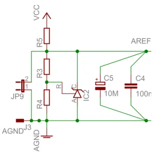
In the following chapters the required precision of an ADC will be discussed, as well as the supporting circuitry such as voltage reference and protection on ADC inputs.
The need to use an ADC comes from the fact that the charging logic will be implemented using a program running on a microcontroller chip. Its selection will not be described in this chapter, as there is a possibility to use dedicated ADC or one integrated in a microcontroller. This decision process will be mentioned in a section about choosing the microcontroller (2.1.5).
Required Precision
The resolution required for an ADC can be determined according to a maximum error that is acceptable for the measurement. This error can be compared to quanti-zation errors for a several ADC resolutions and the resolutions that produce smaller errors can be chosen. Of course the quantization error is not the only error the ADC produces. There are errors due to Differential nonlinearity, Integral nonlinearity and others as well. These depend on the exact device used, so they will be considered upon selection of an exact device from a set of particular type (such as 10-bit or 12-bit ADCs).
The required precision depends on maximum allowable error of these measure-ments:
• battery voltage measurement, • PV voltage measurement, and
• voltage measurement for a current measurement circuitry.
Firstly, the battery voltage measurement is considered. The required precision for
a battery voltage monitoring has been found in literature only for the float voltage
(“constant voltage that is applied continuously to a voltaic cell to maintain the cell
in a fully charged condition” [18]). This value is ±0.05V [5]. As this is probably the
most critical part of charging cycle, this value is considered as satisfactory for all phases of charging cycle.
The maximum absolute error on the battery terminal has to be recalculated to a maximum quantization error on an ADC’s input, because a voltage divider will be used on ADC input:
𝛿BAT=
∆𝑉
𝑉 =
0.05V
15V = 0.00¯3 = 0.¯3%, (2.6)
∆𝑉ADC =𝛿BAT·ADC_range= 0.00¯3·2.5 = 8.¯3mV (2.7)
One digit in an 8-bit ADC conversion result when using 2.5V voltage reference corresponds to: ∆𝑉bit= 2.5 28 = 2.5 256 ≈9.77mV (2.8)
The quantization error is equal to half of the smallest unit of resolution, so it is clear that the 8-bit ideal ADC would be satisfactory.
![Fig. 1.1: The diagram of charging stages of lead-acid battery [41]](https://thumb-us.123doks.com/thumbv2/123dok_us/9984889.2895549/16.892.213.721.125.631/fig-diagram-charging-stages-lead-acid-battery.webp)