An Open Platform for Development
of Network Processing Modules
in Reprogrammable Hardware
John W. Lockwood
∗Department of Computer Science
Applied Research Lab
Washington University
1 Brookings Drive
Saint Louis, MO 63130
Phone: (314) 935-4460
Email:
[email protected]Web:
http://www.arl.wustl.edu/arl/projects/fpx/ABSTRACT
Internet routers and firewalls can be enhanced by packet-processing functions implemented in reconfigurable hard-ware. Through the development of the the Field Program-ma-ble Port Extender (FPX), a platform has been built that demonstrate how networking modules can be used for rapid prototype and deployment new features in such hardware. The platform includes high-speed network interfaces, mul-tiple banks of memory, and Field Programmable Gate Ar-ray (FPGA) logic. The platform allows reprogrammable hardware modules to be dynamically installed into a router or firewall through the use of full or partial reprogram-ming of an FPGA. Applications have been developed for the FPX that include Internet packet routing, data queuing, and application-level content modification. These applica-tions have sufficient performance to process packets at the full rate of an Internet backbone.
1.
INTRODUCTION
The demands of the Internet have affected the requirements of networking routers and firewalls in two major ways. Much higher performance so that they can keep pace with the the growing demands for bandwidth. At the same time, these systems need the flexibility to implement new features and functionality.
1.1
The Need for Bandwidth
Bandwidth on the Internet has greatly increased. With the wide-scale deployment of fiber to business and Asymmetric Digital Subscriber Lines (ADSL) and cable modems to the home; broadband services are now widely available. The combined effect of higher bandwidth to each user, along with ∗This research is supported by NSF: ANI-0096052 and Xil-inx Corp.
larger base of installed users, doubles the bandwidth of the Internet nearly every 100 days.
1.2
Advanced Packet Processing
In order to be competitive, Internet Service Providers (ISPs) must provide their customers with more advanced services than the best-effort packet delivery. Quality of Service (QoS)-enabled routing is needed to support real-time services, such as audio and video conferencing. Firewall services and com-plex port filtering mechanisms are needed to protect net-works from hackers that launch denial of service attacks.
1.3
Software vs Hardware
Software-based based routers and firewalls excel in their ability to implement new reprogrammable features. These features can be added or removed in the router by upgrad-ing the code in the system. The sequential nature of the microprocessor that executes that code, however, can limit the throughput of the system. Application-Specific Inte-grated Circuits (ASICs) are typically used in routers to im-plement these performance-critical features. The static na-ture of an ASIC circuit, however, limits the functionality of the performance-critical features to a fixed set of features.
1.4
Field Programmable Gate Arrays
Field Programmable Gate Arrays can be used to simulta-neously address both of these issues. Routers and firewalls that utilize FPGAs can implement a desirable balance be-tween performance and flexibility [1]. They share the per-formance advantage of ASICs in that customized pipelines can be implemented and that parallel logic functions can be performed over the area of the device
Card OC3/ OC12/ OC48 Line
FPX
ExtenderPort programmableField− Card OC3/ OC12/ OC48 Line Internet UsersFigure 1: FPX in Standalone Configuration, for use as an Internet firewall or packet filter
1.5
Project Background
Field Programmable Gate Arrays have proven to be an ef-fective technology for implementation of networking hard-ware. In the development of the iPOINT testbed, a com-plete Asynchronous Transfer Mode (ATM) switch was built using FPGAs [2]. This system utilized a Xilinx 4013 FPGA to implement a single-stage switch [3] and multiple Xilinx 4005 FPGAs to implement queuing modules at each of the inputs of the switch [4]. The Illinois Input Queue (iiQueue) was implemented to enhance the performance of distributed input queuing by sorted packets according to their flow, des-tination, and priority. A prototype of this system was im-plemented using Xilinx XC4013 FPGAs [5].
The benefit of using reprogrammable logic in the iiQueue was that complex algorithms for queuing data could be tuned by simply reprogramming the FPGA logic. Further, the reprogrammable logic enabled additional packet processing features to be integrated into the same FPGA devices that controlled the queuing circuits.
FPGAs have also proven to be effective for implementation of “bit-intensive” functions networking, such as Forward Er-ror Correction (FEC). FPGAs have also been used as mod-ules in systems, where a software controller is used to load and unload functionality [6].
The use of modules is a common theme in the research area of active networking. An interesting extension to that body of work relates to the integration of the reprogrammable functions in both software and hardware [7].
2.
THE FPX PLATFORM
Through a University research program, a platform called the Field Programmable Port Extender (FPX) has been de-veloped. The FPX enables the rapid prototype and deploy-ment of packet processing modules in reprogrammable hard-ware. The development of this system has provided insight into several design aspects of reprogrammable networking systems, which are discussed in this paper.
3.
DATA FORMAT
Data can be transported over a network in a variety of for-mats. The FPX process data formatted in cells or packets. Cells that are processed by the FPX are assumed to be in the format of Asynchrounous Transfer Mode. Internet packets are assumed to be in the format of an encapsulated frame carried over a Adaptation Layer Five [8].
3.1
Network Topology
OPP IPP IPP OPP OPP OPP IPP IPP Fabric Switch Gigabit Card OC3/ OC12/ OC48 LineFPX
ExtenderPort programmableField−WUGS
FPX
ExtenderPort Field− programmable Card OC3/ OC12/ OC48 LineFigure 2: FPX between Line Card and switch backplane, for use in a router
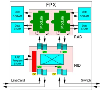
SRAM Module VC VC VC VC RAD NID Module EC EC
FPX
LineCard Switch SRAM SDRAM SDRAM Data Data SRAM Data Program RAD DataFigure 3: NID and RAD Configuration
The FPX can be used by itself or in conjunction with a network switch. In either case, the FPX resides between standard network interfaces found on a line card or switch. Utopia-like interfaces are used to transmit data to and from the interfaces of the FPX.
In the standalone configuration, the FPX interfaces to the ports of optical line card as shown in Figure 1. This con-figuration is typical of an Internet firewall, where one port is routed to the Internet (or Internet Service Provider), and the other leads to a user (or customer network).
In a router configuration, FPX modules reside between a switch fabric and each of the line cards. Currently, the FPX is used as a component in the Washington University Giga-bit Switch (WUGS) [9]. Physically, the module is inserted between an optical line card and the WUGS gigabit switch backplane. The aggregate throughput of the system scales with the number of switch ports.
3.2
Logical Configuration
The FPX implements all logic using two FPGA devices: the Network Interface Device (NID) and the Reprogrammable Application Device (RAD). The interconnection of the RAD and NID to the network and memory components is shown in Figure 3.
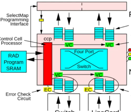
SRAM ProgrammingSelectMap Interface EC EC VC VC Four Port Switch ccp Error Check VC VC Control Cell Asynchronous LineCard Switch Interface Circuit Interface Processor Synch, Buffered NID Lookup Table RAD Virtual Circuit RAD Program
Figure 4: Network Interface Device Configuration
The RAD contains the modules that implement customized packet processing functions. Each module on the RAD con-nects to one Static RAM (SRAM) and to one, wide Syn-chronous Dynamic RAM (SDRAM). In total, the modules implemented on the RAD have full control over four inde-pendent banks of memory. The SRAM is typically used for applications that need to implement table lookup operations (like the Fast IP lookup algorithm), while the SDRAM in-terface is intended for applications like packet queuing that need only transfer bursts of data and can tolerate a higher memory latency.
The RAD communicates with the NID using the same Utopia-like interface as the NID to the network interfaces. Packets on this interface are segmented into a sequence of fixed-size cells that are formatted as IP over ATM. Each interface has a small amount of buffering and implements flow control. A Start of Cell (SOC) signal is asserted to indicate the arrival of data, and the Transmit Cell Available (TCA) signal is as-serted back towards the data source to indicate downstream congestion.
3.3
Network Interface Device
The Network Interface Device (NID) on the FPX controls how packet flows are routed to and from modules. It also provides mechanisms to dynamically load hardware modules over the network and into the router. The combination of these features allows these modules to be dynamically loaded without affecting the switching of other traffic flows or the processing of packets by the other modules in the system. As shown in Figure 4, The NID has several components, all of which are implemented in FPGA hardware. It contains a four-port switch to transfer data between ports;Virtual Cir-cuit lookup tables(VC) on each port in order to selectively route flows; aControl Cell Processor(CP), which is used to process control cells that are transmitted and received over the network; logic to reprogram the FPGA hardware on the RAD; and synchronous and asynchronous interfaces to the four network ports that surround the NID.
3.3.1
Per Flow Routing
The NID routes flows among the two modules on the RAD,
... ... VPI 1023 d4 VCI 1022 VCI 0 VCI 1023+ VPI 1 d1 d3 Table d1 d2 d3 d4 d1 d2 d3 d4 d1 d2 d3 d4 Per−Flow d2 Routing Table d1 d2 d3 d4 Aggregate Flow Routing Table NID Flow Routing
Figure 5: Per-flow routing on the NID
the network interface to the switch, and the network inter-face to the line card using a four-port switch. Each traffic flow that arrives on any incoming port can be forwarded to any destination port.
Each of the NID’s four interfaces provide a small amount of buffering for short-term congestion. Buffers on the NID are implemented using on-chip memory. When packets con-tend for transmission to the same destination port, the NID performs arbitration. For long term congestion, the NID avoids data loss by sending a back-pressure signals to source causing congestion in the outgoing flow. The design of the four-port switch and scheduling algorithm used to arbitrate among flows is based on the design of the iPOINT switch [2] [3].
The NID supports forwarding for both aggregate traffic flows and individual traffic flows. IP Packets are routed through the FPX and switch based on assignment of cell headers that transport that packet. The NID’s Virtual Circuit lookup table (VC) maps these flows into next-hop destinations at each of the four ports. As shown in Figure 5, the NID’s flow routing table contains entries for each of the four ports in the switch that identify the destination port (d1. . . d4) of each flow. The table has sufficient entries to support more than a thousand flows for aggregate traffic and another thousand entries for individual flows.
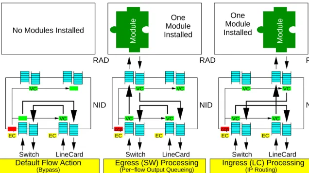
Examples that illustrate the NID’s switching functionality are shown in Figure 6. By default, cells are simply passed between the line card interface and the switch. To imple-ment egress flow processing (i.e., process packets as they exit the router), the NID routes a flow from the switch, to a RAD module, then out to the line card. Likewise, to implement ingress cell processing, the NID routes a virtual circuit from the line card, to a RAD module, then out to the switch. Full RAD processing occurs when data is processed in both directions by both modules on the RAD. Loopback and partial loopback testing can be programmed on the NID to debug experimental modules. Modules can implement selective packet forwarding by reassignment of the headers that transport each packet.
3.3.2
Control functions
The NID implements a Control Cell Processor (CCP) in hardware to manage the operation of the FPX and commu-nicate over the network. On the ingress interface from the switch, the CCP listens to responds to commands that are sent on a specific virtual circuit. The NID processes com-mands that include: (1) modification of per-flow routing entries; (2) reading and writing of hardware status regis-ters, (3) reading and writing of configuration memory, and (4) commands that cause the logic on the RAD to be
repro-VC VC
Module
ECModule
Module
VCRAD
VC EC ccp VC EC ccp VC EC VC VC VCModule
VCModule
VC ccp EC EC ccp VC VC VC EC VC ccp VC EC VC VCModule
Module
VC ECModule
EC VC VC VC EC ccp VC EC VC LineCard SwitchNID
LineCard SwitchNID
NID
LineCard SwitchNID
Switch SwitchInstalled
One
Installed
RAD
RAD
RAD
Module
NID
LineCardModule
One
LineCardNID
LineCard SwitchRAD
RAD
No Modules Installed
Full RAD Processing
(Bypass) (Per−flow Output Queueing)
Default Flow Action
Full Loopback Testing
Dual Egress Processing
Ingress (LC) Processing
Egress (SW) Processing
(Chained Modules) (System Test)
(IP Routing)
(Packet Routing and Reassembly)
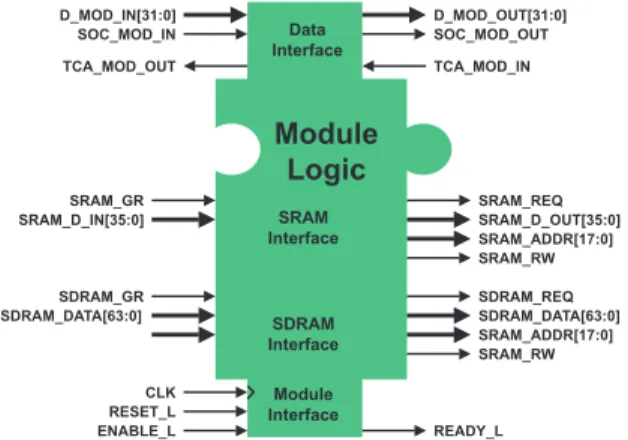
D_MOD_IN[31:0] D_MOD_OUT[31:0] SOC_MOD_OUT SOC_MOD_IN TCA_MOD_IN TCA_MOD_OUT SRAM_D_OUT[35:0] SRAM_ADDR[17:0] SRAM_RW SRAM_REQ SRAM_GR SRAM_D_IN[35:0] SDRAM_DATA[63:0] SRAM_ADDR[17:0] SRAM_RW SDRAM_REQ SDRAM_GR SDRAM_DATA[63:0] CLK RESET_L ENABLE_L READY_L Data Interface SRAM Interface SDRAM Interface Module Interface Module Logic
Figure 7: Modular Component of FPX
grammed. After executing each command, the NID returns a response in a control cell.
3.4
Reprogrammability
In order to reprogram the RAD over the network, the NID implements a reliable protocol to fill the contents of the on-board RAM with configuration data that is sent over the network. As each cell arrives, the NID uses the data and the sequence number in the cell to write data into theRAD Program SRAM. Once the last cell has been correctly re-ceived, and the FPX holds an image of the reconfiguration bytestream that is needed to reprogram the RAD. At that time, another control cell can be sent to NID to initiate the reprogramming of RAD using the contents of theRAD Program SRAM.
The FPX supports partial reprogramming the RAD by al-lowing configuration streams to contain commands that only program a portion of the logic on the RAD. Rather than is-sue a command to reinitialize the device, the NID just writes the frames of reconfiguration data to the RAD’s reprogram-ming port. This feature enables the other module on the RAD to continue processing packets during the partial re-configuration. Similar techniques have been implemented in other systems using software-based controllers [10] [11].
3.5
Modular Architecture
Application-specific functionality is implemented on the RAD as modules. A modular interface has been developed that provides a standard interface to access packet content and to interface with off-chip memory.
Hardware plugin modules on the RAD consist of a region of FPGA gates and internal memory, bounded by a well-defined interface to the network and external memory. Cur-rently, those regions are defined as one half of an FPGA and a fixed set of I/O pins.
3.5.1
Single Module
The modular interface of an FPX component is shown in Figure 7. Data arrives at and departs from a module over a 32-bit wide, Utopia-like interface. Data passes through
FPX
M
odule
FPX
M
odule
FPX
M
odule
SDRAM SRAMIntrachip Module Switching
...
Data
Figure 8: Combined Modules
modules as complete ATM cells. Larger IP datagrams pass through the interface in multiple cells.
The module provides two interfaces to off-chip memory. The SRAM interface supports transfer of 36-bit wide data to and from off-chip SRAM. The Synchronous Dynamic RAM (SDRAM) interface provides a 64-bit wide interface to off-chip memory. In the implementation of the IP lookup mod-ule, the off-chip SRAM is used to store the data structures of the fast IP Lookup algorithm [12].
3.5.2
Combined Modules
As the capacity of FPGAs increases, a larger number of modules can be integrated on the same FPGA. The modular interface on the FPX has been designed so that circuits can retain their same interface, regardless of how many mod-ules are combined into the FPGA. A configuration of an FPX module with three modules mapped into one-half of the RAD is shown in Figure 8.
4.
IMPLEMENTATION OF THE FPX
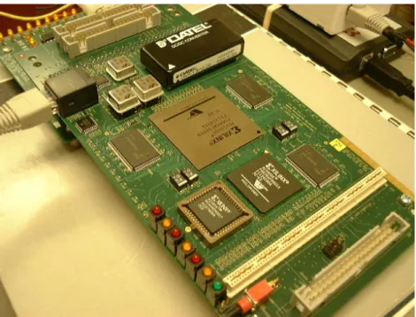
The FPX platform was implemented on the 20 cm ×10.5 cm printed circuit board shown in Figure 9. The FPX in-clude two FPGAs, five banks of memory, and two high-speed network interfaces.
4.1
FPGA Capacity
The FPGAs where chosen so that the system would have sufficient gate capacity to implement meaningful network-ing applications. The RAD is implemented with a Xilinx Virtex 1000E-fg680 FPGA, while the NID is implemented with a Virtex 600E-fg676 FPGA. The NID FPGA contains sufficient logic to interface to the switch and line card, while the larger RAD FPGA was chosen to provide sufficient logic density in order to implement complex IP routing and queu-ing functions.
OSC
100MHz 10 MHzOSC
SDRAM (backside) 8Mbit ZBTSRAM
8Mbit ZBTSRAM
Device
Interface
Network
NID
RAD
Reprogrammable
Application
Device
Virtex1000E fg680
RAD/NID Status SDRAM (backside)SRAM
Program
RAD ReprogOC3 / OC12 / OC48 Linecard Connector
EPROM
NID
62.5 MHz
VRM: 1.8V Switcher
JTAG
WUGS Switch Backplane Connector
FPX
WashU / ARL July, 2000
JL / MR
OSC
Figure 9: FPX Printed Circuit Board
Optics Fiber Pigtail
Line Card
IPP/OPP WUGS Switch Elements IPP/OPP
WUGS
Figure 10: Original configuration of WUGS backplane with line card (side view)
IPP/OPP WUGS Switch Elements IPP/OPP
Optics Fiber Pigtail
WUGS
FPX
Line Card
SDRAM NID FPGA RAD FPGA SRAMs VRMFigure 12: FPX Module
4.2
FPX Memory Configuration
The FPX contains five independent banks of memory. The NID includes a single bank of SRAM, which is used to store configuration data for the RAD. The RAD interfaces to dual banks of SRAM and SDRAM memory.
Two banks of 36-bit wide SRAM were determined sufficient to maintain pointers and data structures needed for Internet packet lookups and management of per-flow queuing data structures. The SRAM on the FPX utilizes Zero Bus Turn-around (ZBT) SRAMs to provide full-throughput.
Two banks of 64-bit wide Synchronous Dynamic Random Access Memory (SDRAM) provide sufficient bandwidth to buffer data to and from the network. At Gigabit/second rates, several Megabytes of memory are required to buffer bursts of data. SDRAM is well suited to meet these require-ments.
The total number of memory operations that can be used to process a packet depend on the Line Card rate and the length of the packet. The faster the link, the fewer the number of cycles: Fifty-six bytes is the smallest packet that would be processed by the WUGS switch/router. This size is slightly larger than the 53-byte size of an Asynchrounous Transfer Mode (ATM) cell.
For memories that operate at 100 MHz and for line cards that operate at OC3 rates (155 Mbits/second), each memory provides 53∗8/155M = 273 operations per cell. The four parallel banks of memory can, therefore, perform a total of 273∗4 = 1092 memory operations within the time period of a cell slot. At OC12 (622 Mbits/second), the same hardware can implement 273 operations. At OC48 (2.4 Gbits/second), the FPX provides 68 memory operations per slot period. Of these operations, 56/8 = 7 writes to the SDRAM memory are used to enqueue a cell, and 56/8 = 7 reads from the
SDRAM are used to dequeue a cell. All remaining memory operations can be used to implement the routing and buffer management functions.
4.3
Networking Interfaces
Networking interfaces on the FPX were optimized to en-able the simultaneous arrival and departure of data cells at SONET OC48 rates. This is the equivalent bandwidth of multiple channels of Gigabit Ethernet.
Physically, the networking interfaces on the FPX were im-plemented in a way that allows the card to be stacked be-tween the line card and backplane of a switch fabric. Fig-ure 10 shows the original configuration of the backplane switch and a line card, while Figure 11 shows the same with the addition of the addition of a FPX module.
4.4
Complete System
A photograph of the FPX module is shown in Figure 12. SRAM components on the FPX are mounted above and be-low the RAD. SDRAM memories are mounted on the back of the FPX in sockets. Reconfiguration data for the FPGAs are stored both in non-volatile Flash memory for the NID and SRAM memory for the RAD.
Figure 13 shows an FPX mounted in one port of the Wash-ington University Gigabit Switch (WUGS) [9]. By inserting FPX modules at each port of the switch, parallel FPX units can be used to simultaneously process packets on all ports of the network switch.
5.
APPLICATIONS
mod-Figure 13: Photo of FPX mounted in WUGS Switch .. Payload .. P45 P47 P44 P46 .. Payload .. Compare Write P45 P47 P44 P46 Match+ [48 bytes in 12 words] Header [5 bytes in 2 words] Payload ’H’ ’E’ ’L’ ’L’ ’O’ ’ ’ ’W’ ’O’ PAD ’R’ ’L’ ’D’ ’.’ ’H’ ’E’ ’L’ ’L’ ’O’ VPI VCI=5 PAD VPI=X P8 P9 P10 P11 P6 P7 P5
...
Copy 32 bits Copy Write Match Match...
JWL:ARL 07/00 VCI=5Figure 14: Cell processing for matching cell
ules on the FPX. The Reprogrammable Application Device is used to implement the user-defined logic. Thus far, Mod-ules have been developed for the FPX that implement IP packet routing [12], packet buffering, and application-level packet content modification. Additional hardware modules can be easily implemented on the FPX. The architecture of the FPX makes it well suited to implement applications like per-flow queuing [5], and flow control algorithms [13] in hardware.
5.1
String Matching Operations
An application called “Hello, World” illustrates how an an FPX module can be implemented to perform application-level content modification. “Hello” searches an ATM cell on particular virtual circuit for a payload starting with the string “HELLO”. If and only if a match was found, the cir-cuit concatenates the content of the cell with the string “WORLD.” A diagram of the formatted cell is shown in Figure 14.
There are several cases in which the cell may not match.
P44 P46 .. Payload .. P45 P47 P44 P46 .. Payload .. Compare +Copy P45 P47 Mismatch ’M’ ’E’ ’L’ ’L’ ’O’ PAD ’M’’E’ ’L’ ’L’ ’O’ VPI PAD VPI=X P8 P9 P10 P11 P6 P7 P5
...
Copy VCI=5 P5 P6 P7 P8 P9 P10 P11 Match...
JWL:ARL 07/00 VCI=5 CopyFigure 15: Cell processing for mismatched payload
First, cells should only be processed if they arrive on the correct virtual circuit. In this example, the module is pro-grammed to process cells on VCI=5. If the VCI doesn’t match, the cell should passes through without modification. Second, for those cells that do arrive on the correct VCI, the string must match over all words in the payload. For the string shown in Figure 15, a mismatch is found in the the first byte of the first word. Since the ”MELLO” doesn’t match ”HELLO”, the contents of the cell are left unchanged. Performing a string match on the FPX is slightly compli-cated by the fact that the payload arrives as a stream of words; not all at once. Since an FPX module receives only one word per clock cycle, the circuit must know the status of previous comparisons to ensure that all current and pre-vious words matched before it writes the word ”WORLD.” in the current and future clock cycles.
5.1.1
Logical Implementation
There are several ways to implement the “Hello World” cir-cuit on the FPX. One such implementation uses a counter
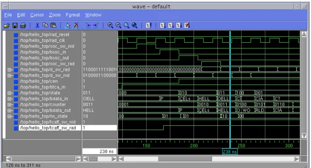
Figure 17: Post-synthesis signal timing relationships VCI Match Reset Check’Hell’ ’O’ Check Dout New Cell World Append "WORLD" to payload
Figure 16: State machine for the Hello World circuit
and the state machine shown in Figure 16. The module be-gins in the reset state. When a new cell arrives, it compares the value of the VCI. If the VCI doesn’t match, it jumps to the ‘Dout’ state. In the ‘Dout’ state, all of the remain-ing data in the cell is written out of the module with the same value it had when it arrived. If the VCI does match, the circuit next scans the first word of the payload for the first four letters of the letters of the string. For cells that do match, the state machine jumps to the ’World’ state. It stays in this state for multiple clock cycles as the content of packet is modified to contain the ”WORLD” string.
5.1.2
Module Operation
The post-synthesis timing relationships among the signals in the ”Hello World” are shown in Figure 17. Data arrives as cells on the 32-bit data bus on switch-side of the RAD logic. The arrival of a new cell on the bus is indicated by the StartOfCell (SOC) signal. The ’Start of Cell (SOC)’ and data, are buffered both internally and across the edge flops of the FPGA. The operation of the circuit can be seen by observing how the buffered output data (bdata out) is
modified from the buffered data input (bdata in). Observe that the hardware module changed the content of the cell from “HELLOELLO...” to “HELLO WORLD”.
5.1.3
Results of Physical Implementation
The circuit to implement the ”Hello World” module was synthesized for he RAD FPGA (a Xilinx V1000E-FG680-7 device) using Exemplar and Xilinx back-end synthesis tools. The resulting circuit operates at: 119 MHz. The 8.4ns criti-cal path in this circuit is well within the 10ns period provided by the RAD’s clock. Since the circuit can handle back-to-back cells; this circuit achieves the maximum packet process-ing rate of (100 MHz)/(14 Clocks/Cell)=7.1 Million packets per second.
The utilization of the FPGA to implement this circuit was 49 out of 12,288 slices on the FPGA. Thus, all of the logic to perform the search and replacement operation for this module was implemented in less than one-half of one percent of the chip resources.
A full report on the implementation of the Hello World mod-ule is available on-line [14]. The full VHDL source code and I/O pin mappings on the RAD can be downloaded from the project website [15].
6.
CONCLUSIONS
Field Programmable Gate Arrays can have an important role in network routers and firewalls. Through the devel-opment of the FPX, a platform has been built that enables features to be implemented in a router or firewall as generic, reprogrammable hardware modules.
The use of the modular interface to implement the functional components has several benefits. First, it provides hardware developers a well-defined interface for receiving and trans-mitting data between the network interfaces and off-chip memories. Second, it allows multiple modules to be eas-ily integrated together. Lastly, due to the reprogrammable nature of the FPGA, it allows all functions of the router or firewall to dynamically upgraded. The FPX allows this function to happen over a network.
Core functionality on the FPX is implemented on the the Networking Interface Device. It forwards traffic between modules; it reliably transports byte-streams over a network; and it implements the logic to dynamically reconfigure an FPGA device.
Several networking modules have been developed for the FPX, including IP routing, data queuing, and application-level packet modification. These applications demonstrated that such a system can efficiently implement performance-critical networking functions.
7.
ACKNOWLEDGMENTS
Contributors to this work include Jon S. Turner, Naji Naufel, David E. Taylor, and David Lim of Washington University and Dave Parlour of Xilinx.
8.
REFERENCES
[1] S. Hauck, “The roles of FPGAs in reprogrammable sys-tems,” Proceedings of the IEEE, vol. 86, pp. 615–638, Apr. 1998.
[2] “Illinois Pulsar-based Optical Interconnect (iPOINT) Homepage.” http://ipoint.vlsi.uiuc.edu, Sept. 1999.
[3] J. W. Lockwood, H. Duan, J. J. Morikuni, S. M. Kang, S. Akkineni, and R. H. Campbell, “Scalable op-toelectronic ATM networks: The iPOINT fully func-tional testbed,”IEEE Journal of Lightwave Technology, pp. 1093–1103, June 1995.
[4] H. Duan, J. W. Lockwood, and S. M. Kang, “FPGA prototype queueing module for high performance ATM switching,” in Proceedings of the Seventh An-nual IEEE International ASIC Conference, (Rochester, NY), pp. 429–432, Sept. 1994.
[5] H. Duan, J. W. Lockwood, S. M. Kang, and J. Will, “High-performance OC-12/OC-48 queue design pro-totype for input-buffered ATM switches,” in INFO-COM’97, (Kobe, Japan), pp. 20–28, Apr. 1997. [6] W. Marcus, I. Hadzic, A. McAuley, and J. Smith,
“Protocol boosters: Applying programmability to net-work infrastructures,” IEEE Communications Maga-zine, vol. 36, no. 10, pp. 79–83, 1998.
[7] S. Choi, J. Dehart, R. Keller, J. Lockwood, J. Turner, and T. Wolf, “Design of a flexible open platform for high performance active networks,” in Allerton Con-ference, (Champaign, IL), 1999.
[8] M. Laubach and J. Halpern, “Classical IP and ARP over ATM.” RFC 2225, Apr. 1998.
[9] J. S. Turner, T. Chaney, A. Fingerhut, and M. Flucke, “Design of a Gigabit ATM switch,” in INFOCOM’97, 1997.
[10] W. Westfeldt, “Internet reconfigurable logic for creating web-enabled devices.” Xilinx Xcell, Q1 1999.
[11] S. Kelem, “Virtex configuration architecture advanced user’s guide.” Xilinx XAPP151, Sept. 1999.
[12] J. W. Lockwood, J. S. Turner, and D. E. Taylor, “Field programmable port extender (FPX) for distributed routing and queuing,” inFPGA’2000, (Monterey, CA), pp. 137–144, Feb. 2000.
[13] M. Bossardt, J. W. Lockwood, S. M. Kang, and S.-Y. Park, “Available bit rate architecture and simulation for an input-buffered and per-vc queued ATM switch,” in GLOBECOM’98, (Sydney, Australia), pp. 1817– 1822, Nov. 1998.
[14] J. Lockwood and D. Lim, “Hello World: A simple application for the field programmable port extender (FPX),” tech. rep., WUCS-00-12, Washington Univer-sity, Department of Computer Science, July 11, 2000. [15] “Field Programmable Port Extender Homepage.”
http://www.arl.wustl.edu/projects/fpx/, Aug. 2000.

![Figure 13: Photo of FPX mounted in WUGS Switch .. Payload .. P45 P47P44P46.. Payload ..Compare WriteP45P47P44P46 Match+[48 bytes in12 words]Header[5 bytes in2 words]Payload’H’ ’E’ ’L’ ’L’’O’ ’ ’ ’W’ ’O’PAD’R’ ’L’ ’D’ ’.’’H’ ’E’ ’L’ ’L’’O’VPIVCI=5PADVPI=XP8](https://thumb-us.123doks.com/thumbv2/123dok_us/1324902.2677101/8.918.218.699.77.402/figure-mounted-switch-payload-payload-compare-writep-payload.webp)