AV-51001 Subscribe Send Feedback
The Arria® V device family consists of the most comprehensive offerings of mid-range FPGAs ranging from the lowest power for 6 gigabits per second (Gbps) and 10 Gbps applications, to the highest mid-range FPGA bandwidth 12.5 Gbps transceivers.
The Arria V devices are ideal for power-sensitive wireless infrastructure equipment, 20G/40G bridging, switching, and packet processing applications, high-definition video processing and image manipulation, and intensive digital signal processing (DSP) applications.
Related Information
Arria V Device Handbook: Known Issues
Lists the planned updates to the Arria V Device Handbook chapters.
Key Advantages of Arria V Devices
Table 1: Key Advantages of the Arria V Device Family
Advantage Supporting Feature
Lowest static power in its
class • Built on TSMC's 28 nm process technology and includes an abundance ofhard intellectual property (IP) blocks • Power-optimized MultiTrack routing and core architecture
• Up to 50% lower power consumption than the previous generation device
• Lowest power transceivers of any midrange family Improved logic integration
and differentiation capabil‐ ities
• 8-input adaptive logic module (ALM)
• Up to 38.38 megabits (Mb) of embedded memory • Variable-precision digital signal processing (DSP) blocks Increased bandwidth
capacity • Serial data rates up to 12.5 Gbps• Hard memory controllers Hard processor system
(HPS) with integrated ARM® Cortex™-A9 MPCore processor
• Tight integration of a dual-core ARM Cortex-A9 MPCore processor, hard IP, and an FPGA in a single Arria V system-on-a-chip (SoC) • Supports over 128 Gbps peak bandwidth with integrated data coherency
between the processor and the FPGA fabric
© 2015 Altera Corporation. All rights reserved. ALTERA, ARRIA, CYCLONE, ENPIRION, MAX, MEGACORE, NIOS, QUARTUS and STRATIX words and logos are
trademarks of Altera Corporation and registered in the U.S. Patent and Trademark Office and in other countries. All other words and logos identified as
Advantage Supporting Feature Lowest system cost • Requires as few as four power supplies to operate
• Available in thermal composite flip chip ball-grid array (BGA) packaging • Includes innovative features such as Configuration via Protocol (CvP),
partial reconfiguration, and design security
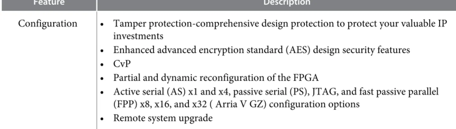
Summary of Arria V Features
Table 2: Summary of Features for Arria V Devices
Feature Description
Technology • TSMC's 28-nm process technology:
• Arria V GX, GT, SX, and ST—28-nm low power (28LP) process • Arria V GZ—28-nm high performance (28HP) process
• Lowest static power in its class (less than 1.2 W for 500K logic elements (LEs) at 85°C junction under typical conditions)
• 0.85 V, 1.1 V, or 1.15 V core nominal voltage Packaging • Thermal composite flip chip BGA packaging
• Multiple device densities with identical package footprints for seamless migration between different device densities
• Leaded(1), lead-free (Pb-free), and RoHS-compliant options High-performance
FPGA fabric • Enhanced 8-input ALM with four registers• Improved routing architecture to reduce congestion and improve compilation time Internal memory
blocks • M10K—10-kilobits (Kb) memory blocks with soft error correction code (ECC)( Arria V GX, GT, SX, and ST devices only) • M20K—20-Kb memory blocks with hard ECC ( Arria V GZ devices only) • Memory logic array block (MLAB)-640-bit distributed LUTRAM where you can
use up to 50% of the ALMs as MLAB memory
(1) Contact Altera for availability.
Embedded Hard IP blocks
Variable-precision
DSP • Native support for up to four signal processing precisionlevels: • Three 9 x 9, two 18 x 18, or one 27 x 27 multiplier in the
same variable-precision DSP block
• One 36 x 36 multiplier using two variable-precision DSP blocks ( Arria V GZ devices only)
• 64-bit accumulator and cascade for systolic finite impulse responses (FIRs)
• Embedded internal coefficient memory • Preadder/subtractor for improved efficiency Memory controller
( Arria V GX, GT, SX, and ST only)
DDR3 and DDR2
Embedded
transceiver I/O • Custom implementation:• Arria V GX and SX devices—up to 6.5536 Gbps • Arria V GT and ST devices—up to 10.3125 Gbps • Arria V GZ devices—up to 12.5 Gbps
• PCI Express® (PCIe®) Gen2 (x1, x2, or x4) and Gen1 (x1, x2, x4, or x8) hard IP with multifunction support, endpoint, and root port
• PCIe Gen3 (x1, x2, x4, or x8) support ( Arria V GZ only) • Gbps Ethernet (GbE) and XAUI physical coding sublayer
(PCS)
• Common Public Radio Interface (CPRI) PCS
• Gigabit-capable passive optical network (GPON) PCS • 10-Gbps Ethernet (10GbE) PCS ( Arria V GZ only) • Serial RapidIO® (SRIO) PCS
• Interlaken PCS ( Arria V GZ only) Clock networks • Up to 650 MHz global clock network
• Global, quadrant, and peripheral clock networks
• Clock networks that are not used can be powered down to reduce dynamic power Phase-locked loops
(PLLs) • High-resolution fractional PLLs• Precision clock synthesis, clock delay compensation, and zero delay buffering (ZDB)
• Integer mode and fractional mode
Feature Description FPGA
General-purpose I/Os (GPIOs)
• 1.6 Gbps LVDS receiver and transmitter • 800 MHz/1.6 Gbps external memory interface • On-chip termination (OCT)
• 3.3 V support (2) External Memory
Interface Memory interfaces with low latency:• Hard memory controller-up to 1.066 Gbps • Soft memory controller-up to 1.6 Gbps Low-power
high-speed serial interface • 600 Mbps to 12.5 Gbps integrated transceiver speed• Less than 105 mW per channel at 6 Gbps, less than 165 mW per channel at 10 Gbps, and less than 170 mW per channel at 12.5 Gbps
• Transmit pre-emphasis and receiver equalization • Dynamic partial reconfiguration of individual channels
• Physical medium attachment (PMA) with soft PCS that supports 9.8304 Gbps CPRI ( Arria V GT and ST only)
• PMA with hard PCS that supports up to 9.8 Gbps CPRI ( Arria V GZ only) • Hard PCS that supports 10GBASE-R and 10GBASE-KR ( Arria V GZ only) HPS
( Arria V SX and ST devices only)
• Dual-core ARM Cortex-A9 MPCore processor—up to 1.05 GHz maximum frequency with support for symmetric and asymmetric multiprocessing • Interface peripherals—10/100/1000 Ethernet media access control (EMAC),
USB 2.0 On-The-GO (OTG) controller, quad serial peripheral interface (QSPI) flash controller, NAND flash controller, Secure Digital/MultiMediaCard (SD/ MMC) controller, UART, serial peripheral interface (SPI), I2C interface, and up to 85 HPS GPIO interfaces
• System peripherals—general-purpose timers, watchdog timers, direct memory access (DMA) controller, FPGA configuration manager, and clock and reset managers
• On-chip RAM and boot ROM
• HPS–FPGA bridges—include the FPGA-to-HPS, HPS-to-FPGA, and lightweight HPS-to-FPGA bridges that allow the FPGA fabric to issue transactions to slaves in the HPS, and vice versa
• FPGA-to-HPS SDRAM controller subsystem—provides a configurable interface to the multiport front end (MPFE) of the HPS SDRAM controller
• ARM CoreSight™ JTAG debug access port, trace port, and on-chip trace storage
(2) Arria V GZ devices support 3.3 V with a 3.0 V V .
Configuration • Tamper protection-comprehensive design protection to protect your valuable IP investments
• Enhanced advanced encryption standard (AES) design security features • CvP
• Partial and dynamic reconfiguration of the FPGA
• Active serial (AS) x1 and x4, passive serial (PS), JTAG, and fast passive parallel (FPP) x8, x16, and x32 ( Arria V GZ) configuration options
• Remote system upgrade
Arria V Device Variants and Packages
Table 3: Device Variants for the Arria V Device FamilyVariant Description
Arria V GX FPGA with integrated 6.5536 Gbps transceivers that provides bandwidth, cost, and power levels that are optimized for high-volume data and signal-processing applica‐ tions
Arria V GT FPGA with integrated 10.3125 Gbps transceivers that provides enhanced high-speed serial I/O bandwidth for cost-sensitive data and signal processing applications
Arria V GZ FPGA with integrated 12.5 Gbps transceivers that provides enhanced high-speed serial I/O bandwidth for high-performance and cost-sensitive data and signal processing applications
Arria V SX SoC with integrated ARM-based HPS and 6.5536 Gbps transceivers Arria V ST SoC with integrated ARM-based HPS and 10.3125 Gbps transceivers
Arria V GX
This section provides the available options, maximum resource counts, and package plan for the Arria V GX devices.
The information in this section is correct at the time of publication. For the latest information and to get more details, refer to the Altera Product Selector.
Related Information
Altera Product Selector
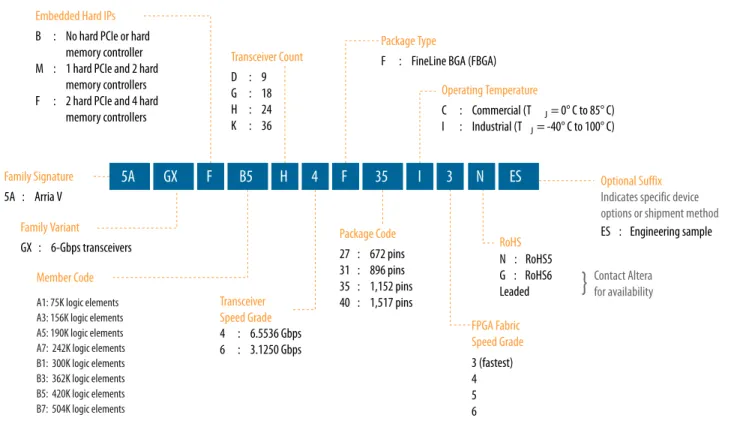
Available Options
Figure 1: Sample Ordering Code and Available Options for Arria V GX Devices
Family Signature Embedded Hard IPs
Transceiver Count Transceiver Speed Grade Package Type Package Code Operating Temperature FPGA Fabric Speed Grade GX : 6-Gbps transceivers B : No hard PCIe or hard
memory controller M : 1 hard PCIe and 2 hard
memory controllers F : 2 hard PCIe and 4 hard
memory controllers
5A : Arria V
A1: 75K logic elements A3: 156K logic elements A5: 190K logic elements A7: 242K logic elements B1: 300K logic elements B3: 362K logic elements B5: 420K logic elements B7: 504K logic elements D : 9 G : 18 H : 24 K : 36 4 : 6.5536 Gbps 6 : 3.1250 Gbps
F : FineLine BGA (FBGA)
27 : 672 pins 31 : 896 pins 35 : 1,152 pins 40 : 1,517 pins C : Commercial (T J = 0° C to 85° C) I : Industrial (T J = -40° C to 100° C) 3 (fastest) 4 5 6 5A GX F B5 H 4 F 35 I 3 Member Code Family Variant Optional Suffix Indicates specific device options or shipment method RoHS N : RoHS5 G : RoHS6 Leaded ES : Engineering sample ES N
}
Contact Altera for availabilityMaximum Resources
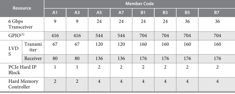
Table 4: Maximum Resource Counts for Arria V GX Devices
Resource Member Code
A1 A3 A5 A7 B1 B3 B5 B7 Logic Elements (LE) (K) 75 156 190 242 300 362 420 504 ALM 28,302 58,900 71,698 91,680 113,208 136,880 158,491 190,240 Register 113,208 235,600 286,792 366,720 452,832 547,520 633,964 760,960 Mem ory (Kb) M10K 8,000 10,510 11,800 13,660 15,100 17,260 20,540 24,140 MLAB 463 961 1,173 1,448 1,852 2,098 2,532 2,906 Variable-precision DSP Block 240 396 600 800 920 1,045 1,092 1,156 18 x 18 Multiplier 480 792 1,200 1,600 1,840 2,090 2,184 2,312 PLL 10 10 12 12 12 12 16 16
Resource A1 A3 A5 A7 B1 B3 B5 B7 6 Gbps Transceiver 9 9 24 24 24 24 36 36 GPIO(3) 416 416 544 544 704 704 704 704 LVD S Transmi tter 67 67 120 120 160 160 160 160 Receiver 80 80 136 136 176 176 176 176 PCIe Hard IP Block 1 1 2 2 2 2 2 2 Hard Memory Controller 2 2 4 4 4 4 4 4 Related Information
High-Speed Differential I/O Interfaces and DPA in Arria V Devices chapter, Arria V Device Handbook
Provides the number of LVDS channels in each device package.
Package Plan
Table 5: Package Plan for Arria V GX Devices
Member Code F672 (27 mm) F896 (31 mm) F1152 (35 mm) F1517 (40 mm)
GPIO XCVR GPIO XCVR GPIO XCVR GPIO XCVR
A1 336 9 416 9 — — — — A3 336 9 416 9 — — — — A5 336 9 384 18 544 24 — — A7 336 9 384 18 544 24 — — B1 — — 384 18 544 24 704 24 B3 — — 384 18 544 24 704 24 B5 — — — — 544 24 704 36 B7 — — — — 544 24 704 36
Arria V GT
This section provides the available options, maximum resource counts, and package plan for the Arria V GT devices.
The information in this section is correct at the time of publication. For the latest information and to get more details, refer to the Altera Product Selector.
Related Information
Altera Product Selector
Provides the latest information about Altera products.
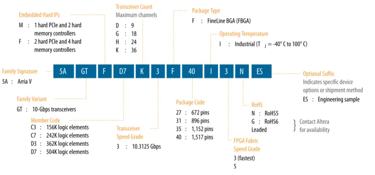
Available Options
Figure 2: Sample Ordering Code and Available Options for Arria V GT Devices
Family Signature
Embedded Hard IPs Transceiver CountMaximum channels
Transceiver Speed Grade Package Type Package Code Operating Temperature FPGA Fabric Speed Grade GT : 10-Gbps transceivers M : 1 hard PCIe and 2 hard
memory controllers F : 2 hard PCIe and 4 hard
memory controllers 5A : Arria V C3 : 156K logic elements C7 : 242K logic elements D3 : 362K logic elements D7 : 504K logic elements D : 9 G : 18 H : 24 K : 36 3 : 10.3125 Gbps
F : FineLine BGA (FBGA)
27 : 672 pins 31 : 896 pins 35 : 1,152 pins 40 : 1,517 pins 3 (fastest) 5 5A GT F D7 K 3 F 40 I 3 Member Code Family Variant I : Industrial (T J = -40° C to 100° C) Optional Suffix Indicates specific device options or shipment method RoHS N : RoHS5 G : RoHS6 Leaded ES : Engineering sample ES N
}
Contact Altera for availabilityMaximum Resources
Table 6: Maximum Resource Counts for Arria V GT Devices
Resource Member Code
C3 C7 D3 D7
Logic Elements (LE) (K) 156 242 362 504
ALM 58,900 91,680 136,880 190,240 Register 235,600 366,720 547,520 760,960 Memory (Kb) M10K 10,510 13,660 17,260 24,140 MLAB 961 1,448 2,098 2,906 Variable-precision DSP Block 396 800 1,045 1,156 18 x 18 Multiplier 792 1,600 2,090 2,312 PLL 10 12 12 16
Resource C3 C7 D3 D7 Transceiver 6 Gbps(4) 3 (9) 6 (24) 6 (24) 6 (36) 10 Gbps(5) 4 12 12 20 GPIO(6) 416 544 704 704 LVDS Transmitter 68 120 160 160 Receiver 80 136 176 176
PCIe Hard IP Block 1 2 2 2
Hard Memory Controller 2 4 4 4
Related Information
• High-Speed Differential I/O Interfaces and DPA in Arria V Devices chapter, Arria V Device
Handbook
Provides the number of LVDS channels in each device package.
• Transceiver Architecture in Arria V Devices
Describes 10 Gbps channels usage conditions and SFF-8431 compliance requirements.
Package Plan
Table 7: Package Plan for Arria V GT Devices
Memb er Code F672 (27 mm) F896 (31 mm) F1152 (35 mm) F1517 (40 mm) GPIO XCVR GPIO XCVR GPIO XCVR GPIO XCVR 6-Gbps Gbps10- Gbps6- Gbps10- Gbps6- Gbps10- Gbps6- 10-Gbps C3 336 3 (9) 4 416 3 (9) 4 — — — — — — C7 — — — 384 6 (18) 8 544 6 (24) 12 — — — D3 — — — 384 6 (18) 8 544 6 (24) 12 704 6 (24) 12 D7 — — — — — — 544 6 (24) 12 704 6 (36) 20
The 6-Gbps transceiver counts are for dedicated 6-Gbps channels. You can also configure any pair of 10-Gbps channels as three 6-10-Gbps channels—the total number of 6-10-Gbps channels are shown in brackets. For example, you can also configure the Arria V GT D7 device in the F1517 package with nine 6-Gbps (4) The 6 Gbps transceiver counts are for dedicated 6-Gbps channels. You can also configure any pair of
10 Gbps channels as three 6 Gbps channels-the total number of 6 Gbps channels are shown in brackets. (5) Chip-to-chip connections only. For 10 Gbps channel usage conditions, refer to the Transceiver Architecture
in Arria V Devices chapter.
and eighteen 10-Gbps, twelve 6-Gbps and sixteen 10-Gbps, fifteen 6-Gbps and fourteen 10-Gbps, or up to thirty-six 6-Gbps with no 10-Gbps channels.
Arria V GZ
This section provides the available options, maximum resource counts, and package plan for the Arria V GZ devices.
The information in this section is correct at the time of publication. For the latest information and to get more details, refer to the Altera Product Selector.
Related Information
Altera Product Selector
Provides the latest information about Altera products.
Available Options
Figure 3: Sample Ordering Code and Available Options for Arria V GZ Devices
Family Signature Embedded Hard IPs
Transceiver Count Maximum channels Transceiver Speed Grade Package Type Package Code Operating Temperature FPGA Fabric Speed Grade Optional Suffix
Indicates specific device options or shipment method
GZ : 12.5-Gbps transceivers M : 1 hard PCIe controller
5A : Arria V E1 : 220K logic elements E3 : 360K logic elements E5 : 400K logic elements E7 : 450K logic elements E : 12 H : 24 K : 36 2 : 12.5 Gbps 3 : 10.3125 Gbps
F : FineLine BGA (FBGA) H : Hybrid FBGA 29 : 780 pins 35 : 1,152 pins 40 : 1,517 pins 3 (fastest) 4 N : Lead-free packaging
Contact Altera for availability of leaded options L : Low-power device 5A GZ M E7 K 2 F 40 C 3 N Member Code Family Variant C : Commercial (T J = 0° C to 85° C) I : Industrial (T J = -40° C to 100° C)
Note: Low-power device option is available only for –3 speed grade at industrial temperature
Maximum Resources
Table 8: Maximum Resource Counts for Arria V GZ Devices
Resource Member Code
E1 E3 E5 E7
Logic Elements (LE) (K) 220 360 400 450
ALM 83,020 135,840 150,960 169,800
Register 332,080 543,360 603,840 679,200
Resource E1 E3 E5 E7 Memory (Kb) M20K 11,700 19,140 28,800 34,000 MLAB 2,594 4,245 4,718 5,306 Variable-precision DSP Block 800 1,044 1,092 1,139 18 x 18 Multiplier 1,600 2,088 2,184 2,278 PLL 20 20 24 24 12.5 Gbps Transceiver 24 24 36 36 GPIO(7) 414 414 674 674 LVDS Transmitter 99 99 166 166 Receiver 108 108 168 168
PCIe Hard IP Block 1 1 1 1
Related Information
High-Speed Differential I/O Interfaces and DPA in Arria V Devices chapter, Arria V Device Handbook
Provides the number of LVDS channels in each device package.
Package Plan
Table 9: Package Plan for Arria V GZ Devices
Member Code H780 (33 mm) F1152 (35 mm) F1517 (40 mm)
GPIO XCVR GPIO XCVR GPIO XCVR
E1 342 12 414 24 — —
E3 342 12 414 24 — —
E5 — — 534 24 674 36
E7 — — 534 24 674 36
Arria V SX
This section provides the available options, maximum resource counts, and package plan for the Arria V SX devices.
The information in this section is correct at the time of publication. For the latest information and to get more details, refer to the Altera Product Selector.
Related Information
Altera Product Selector
Provides the latest information about Altera products.
Available Options
Figure 4: Sample Ordering Code and Available Options for Arria V SX Devices The –3 FPGA fabric speed grade is available only for industrial temperature devices.
Family Signature Embedded Hard IPs
Transceiver Count Transceiver Speed Grade Package Type Package Code Operating Temperature FPGA Fabric Speed Grade Optional Suffix
Indicates specific device options or shipment method SX : SoC with 6-Gbps transceivers
B : No hard PCIe or hard memory controllers M : 1 hard PCIe controllers and
2 hard memory controllers F : 2 hard PCIe controllers and
3 hard memory controllers
5A : Arria V B3 : 350K logic elements B5 : 462K logic elements D : 9 E : 12 G : 18 H : 30 4 : 6.5336 Gbps 6 : 3.125 Gbps F : FineLine BGA (FBGA)
31 : 896 pins 35 : 1,152 pins 40 : 1,517 pins C : Commercial (T J = 0° C to 85° C) I : Industrial (T J = -40° C to 100° C) 3 (fastest) 4 5 6 N : Lead-free packaging Contact Altera for availability of leaded options ES : Engineering sample 5A SX F B5 H 4 F 40 I 3 N Member Code Family Variant
Maximum Resources
Table 10: Maximum Resource Counts for Arria V SX Devices
Resource Member Code
B3 B5
Logic Elements (LE) (K) 350 462
ALM 132,075 174,340 Register 528,300 697,360 Memory (Kb) M10K 17,290 22,820 MLAB 2,014 2,658 Variable-precision DSP Block 809 1,090 18 x 18 Multiplier 1,618 2,180
Resource B3 B5 FPGA PLL 14 14 HPS PLL 3 3 6 Gbps Transceiver 30 30 FPGA GPIO(8) 540 540 HPS I/O 208 208 LVDS Transmitter 120 120 Receiver 136 136
PCIe Hard IP Block 2 2
FPGA Hard Memory Controller 3 3
HPS Hard Memory Controller 1 1
ARM Cortex-A9 MPCore Processor Dual-core Dual-core
Related Information
High-Speed Differential I/O Interfaces and DPA in Arria V Devices chapter, Arria V Device Handbook
Provides the number of LVDS channels in each device package.
Package Plan
Table 11: Package Plan for Arria V SX Devices
The HPS I/O counts are the number of I/Os in the HPS and does not correlate with the number of HPS-specific I/O pins in the FPGA. Each HPS-specific pin in the FPGA may be mapped to several HPS I/Os.
Member Code F896 (31 mm) F1152 (35 mm) F1517 (40 mm) FPGA
GPIO HPS I/O XCVR FPGAGPIO HPS I/O XCVR FPGAGPIO HPS I/O XCVR
B3 250 208 12 385 208 18 540 208 30
B5 250 208 12 385 208 18 540 208 30
Arria V ST
This section provides the available options, maximum resource counts, and package plan for the Arria V ST devices.
The information in this section is correct at the time of publication. For the latest information and to get more details, refer to the Altera Product Selector.
Related Information
Altera Product Selector
Provides the latest information about Altera products.
Available Options
Figure 5: Sample Ordering Code and Available Options for Arria V ST Devices
Family Signature
Embedded Hard IPs Transceiver Count
Maximum channels Transceiver Speed Grade Package Type Package Code Operating Temperature FPGA Fabric Speed Grade Optional Suffix
Indicates specific device options or shipment method ST : SoC with 10-Gbps transceivers
M : 1 hard PCIe controller and 2 hard memory controllers F : 2 hard PCIe controllers and
3 hard memory controllers
5A : Arria V D3 : 350K logic elements D5 : 462K logic elements E : 12 G : 18 K : 30 3 : 10.3125 Gbps
F : FineLine BGA (FBGA)
31 : 896 pins 35 : 1,152 pins 40 : 1,517 pins I : Industrial (T J = -40° C to 100° C) 3 (fastest) 5 N : Lead-free packaging Contact Altera for availability of leaded options ES : Engineering sample 5A ST F D5 K 3 F 40 I 3 N Member Code Family Variant
Maximum Resources
Table 12: Maximum Resource Counts for Arria V ST Devices
Resource Member Code
D3 D5
Logic Elements (LE) (K) 350 462
ALM 132,075 174,340 Register 528,300 697,360 Memory (Kb) M10K 17,290 22,820 MLAB 2,014 2,658 Variable-precision DSP Block 809 1,090 18 x 18 Multiplier 1,618 2,180 FPGA PLL 14 14 HPS PLL 3 3 Transceiver 6-Gbps 30 30 10-Gbps(9) 16 16
Resource D3 D5 FPGA GPIO(10) 540 540 HPS I/O 208 208 LVDS Transmitter 120 120 Receiver 136 136
PCIe Hard IP Block 2 2
FPGA Hard Memory Controller 3 3
HPS Hard Memory Controller 1 1
ARM Cortex-A9 MPCore Processor Dual-core Dual-core
Related Information
• High-Speed Differential I/O Interfaces and DPA in Arria V Devices chapter, Arria V Device
Handbook
Provides the number of LVDS channels in each device package.
• Transceiver Architecture in Arria V Devices
Describes 10 Gbps channels usage conditions and SFF-8431 compliance requirements.
Package Plan
Table 13: Package Plan for Arria V ST Devices
The HPS I/O counts are the number of I/Os in the HPS and does not correlate with the number of HPS-specific I/O pins in the FPGA. Each HPS-specific pin in the FPGA may be mapped to several HPS I/Os.
Memb er Code F896 (31 mm) F1152 (35 mm) F1517 (40 mm) FPGA GPIO HPSI/O XCVR FPGA GPIO HPSI/O XCVR FPGA GPIO HPSI/O XCVR 6 Gbps 10 Gbps 6 Gbps Gbps10 6 Gbps 10 Gbps D3 250 208 12 6 385 208 18 8 540 208 30 16 D5 250 208 12 6 385 208 18 8 540 208 30 16
(9) Chip-to-chip connections only. For 10 Gbps channel usage conditions, refer to the Transceiver Architecture in Arria V Devices chapter.
I/O Vertical Migration for Arria V Devices
Figure 6: Vertical Migration Capability Across Arria V Device Packages and Densities
The arrows indicate the vertical migration paths. Some packages have several migration paths. The devices included in each vertical migration path are shaded. You can also migrate your design across device densities in the same package option if the devices have the same dedicated pins, configuration pins, and power pins.
Variant Member Code Package
F672 F780 F896 F 1152 F1517 Arria V GX A1 A3 A5 A7 B1 B3 B5 B7 Arria V GT C3 C7 D3 D7 Arria V GZ E1 E3 E5 E7 Arria V SX B3 B5 Arria V ST D3 D5
You can achieve the vertical migration shaded in red if you use only up to 320 GPIOs, up to nine 6 Gbps transceiver channels, and up to four 10 Gbps transceiver (for Arria V GT devices). This migration path is not shown in the Quartus Prime software Pin Migration View.
Note: To verify the pin migration compatibility, use the Pin Migration View window in the Quartus Prime software Pin Planner.
Note: Except for Arria V GX A5 and A7, and Arria V GT C7 devices, all other Arria V GX and GT devices require a specific power-up sequence. If you plan to migrate your design from Arria V GX A5 and A7, and Arria V GT C7 devices to other Arria V devices, your design must adhere to the same required power-up sequence.
• Managing Device I/O Pins chapter, Quartus Prime Handbook
Provides more information about vertical I/O migrations.
• Power Management in Arria V Devices
Describes the power-up sequence required for Arria V GX and GT devices.
Adaptive Logic Module
Arria V devices use a 28 nm ALM as the basic building block of the logic fabric.
The ALM, as shown in following figure, uses an 8-input fracturable look-up table (LUT) with four dedicated registers to help improve timing closure in register-rich designs and achieve an even higher design packing capability than previous generations.
Figure 7: ALM for Arria V Devices
FPGA Device 1 2 3 4 5 6 7 8 Adaptive LUT Full Adder Reg Reg Full Adder Reg Reg
You can configure up to 50% of the ALMs in the Arria V devices as distributed memory using MLABs.
Related Information
Embedded Memory Capacity in Arria V Devices on page 20
Variable-Precision DSP Block
Arria V devices feature a variable-precision DSP block that supports these features:
• Configurable to support signal processing precisions ranging from 9 x 9, 18 x 18, 27 x 27, and 36 x 36 bits natively
• A 64-bit accumulator • Double accumulator
• A hard preadder that is available in both 18- and 27-bit modes
• Cascaded output adders for efficient systolic finite impulse response (FIR) filters • Dynamic coefficients
• 18-bit internal coefficient register banks • Enhanced independent multiplier operation
• Efficient support for single-precision floating point arithmetic • The inferability of all modes by the Quartus Prime design software Table 14: Variable-Precision DSP Block Configurations for Arria V Devices
Usage Example Multiplier Size (Bit) DSP Block Resource
Low precision fixed point
for video applications Three 9 x 9 1
Medium precision fixed
point in FIR filters Two 18 x 18 1
FIR filters Two 18 x 18 with accumulate 1
Single-precision
floating-point implementations One 27 x 27 1
Very high precision fixed
point implementations One 36 x 36 2
You can configure each DSP block during compilation as independent three 9 x 9, two 18 x 18, or one 27 x 27 multipliers. Using two DSP block resources, you can also configure a 36 x 36 multiplier for high-precision applications. With a dedicated 64 bit cascade bus, you can cascade multiple variable-high-precision DSP blocks to implement even higher precision DSP functions efficiently.
The table lists the variable-precision DSP resources by bit precision for each Arria V device. Variant Member
Code
Variable-precision DSP Block
Independent Input and Output Multiplications
Operator Multiplier18 x 18
Adder Mode
18 x 18 Multiplier Adder Summed with 36 bit Input 9 x 9
Multiplier Multiplier18 x 18 Multiplier27 x 27 Multiplier36 x 36
Arria V GX A1 240 720 480 240 — 240 240 A3 396 1,188 792 396 — 396 396 A5 600 1,800 1,200 600 — 600 600 A7 800 2,400 1,600 800 — 800 800 B1 920 2,760 1,840 920 — 920 920 B3 1,045 3,135 2,090 1,045 — 1,045 1,045 B5 1,092 3,276 2,184 1,092 — 1,092 1,092 B7 1,156 3,468 2,312 1,156 — 1,156 1,156 Arria V GT C3 396 1,188 792 396 — 396 396 C7 800 2,400 1,600 800 — 800 800 D3 1,045 3,135 2,090 1,045 — 1,045 1,045 D7 1,156 3,468 2,312 1,156 — 1,156 1,156 Arria V GZ E1 800 2,400 1,600 800 400 800 800 E3 1,044 3,132 2,088 1,044 522 1,044 1,044 E5 1,092 3,276 2,184 1,092 546 1,092 1,092 E7 1,139 3,417 2,278 1,139 569 1,139 1,139 Arria V SX B3 809 2,427 1,618 809 — 809 809 B5 1,090 3,270 2,180 1,090 — 1,090 1,090 Arria V ST D3 809 2,427 1,618 809 — 809 809 D5 1,090 3,270 2,180 1,090 — 1,090 1,090
Embedded Memory Blocks
The embedded memory blocks in the devices are flexible and designed to provide an optimal amount of small- and large-sized memory arrays to fit your design requirements.
Types of Embedded Memory
The Arria V devices contain two types of memory blocks:
• 20 Kb M20K or 10 Kb M10K blocks—blocks of dedicated memory resources. The M20K and M10K blocks are ideal for larger memory arrays while still providing a large number of independent ports. • 640 bit memory logic array blocks (MLABs)—enhanced memory blocks that are configured from
dual-purpose logic array blocks (LABs). The MLABs are ideal for wide and shallow memory arrays. The MLABs are optimized for implementation of shift registers for digital signal processing (DSP) applica‐ tions, wide shallow FIFO buffers, and filter delay lines. Each MLAB is made up of ten adaptive logic modules (ALMs). In the Arria V devices, you can configure these ALMs as ten 32 x 2 blocks, giving you one 32 x 20 simple dual-port SRAM block per MLAB. You can also configure these ALMs, in Arria V GZ devices, as ten 64 x 1 blocks, giving you one 64 x 10 simple dual-port SRAM block per MLAB.
Embedded Memory Capacity in Arria V Devices
Table 16: Embedded Memory Capacity and Distribution in Arria V Devices
Variant Member Code
M20K M10K MLAB
Total RAM Bit (Kb) Block RAM Bit
(Kb) Block RAM Bit(Kb) Block RAM Bit(Kb)
Arria V GX A1 — — 800 8,000 741 463 8,463 A3 — — 1,051 10,510 1538 961 11,471 A5 — — 1,180 11,800 1877 1,173 12,973 A7 — — 1,366 13,660 2317 1,448 15,108 B1 — — 1,510 15,100 2964 1,852 16,952 B3 — — 1,726 17,260 3357 2,098 19,358 B5 — — 2,054 20,540 4052 2,532 23,072 B7 — — 2,414 24,140 4650 2,906 27,046 Arria V GT C3 — — 1,051 10,510 1538 961 11,471 C7 — — 1,366 13,660 2317 1,448 15,108 D3 — — 1,726 17,260 3357 2,098 19,358 D7 — — 2,414 24,140 4650 2,906 27,046 Arria V GZ E1 585 11,700 — — 4,151 2,594 14,294 E3 957 19,140 — — 6,792 4,245 23,385 E5 1,440 28,800 — — 7,548 4,718 33,518 E7 1,700 34,000 — — 8,490 5,306 39,306 Arria V SX B3 — — 1,729 17,290 3223 2,014 19,304 B5 — — 2,282 22,820 4253 2,658 25,478
Variant Member Code Block RAM Bit(Kb) Block RAM Bit(Kb) Block RAM Bit(Kb) Total RAM Bit(Kb)
Arria V ST D3 — — 1,729 17,290 3223 2,014 19,304
D5 — — 2,282 22,820 4253 2,658 25,478
Embedded Memory Configurations
Table 17: Supported Embedded Memory Block Configurations for Arria V Devices
This table lists the maximum configurations supported for the embedded memory blocks. The information is applicable only to the single-port RAM and ROM modes.
Memory Block Depth (bits) Programmable Width
MLAB 32 x16, x18, or x20 64(11) x10 M20K 512 x40 1K x20 2K x10 4K x5 8K x2 16K x1 M10K 256 x40 or x32 512 x20 or x16 1K x10 or x8 2K x5 or x4 4K x2 8K x1
Clock Networks and PLL Clock Sources
650 MHz Arria V devices have 16 global clock networks capable of up to operation. The clock network architecture is based on Altera's global, quadrant, and peripheral clock structure. This clock structure is supported by dedicated clock input pins and fractional PLLs.
Note: To reduce power consumption, the Quartus Prime software identifies all unused sections of the clock network and powers them down.
PLL Features
The PLLs in the Arria V devices support the following features: • Frequency synthesis
• On-chip clock deskew • Jitter attenuation • Counter reconfiguration
• Programmable output clock duty cycles • PLL cascading
• Reference clock switchover • Programmable bandwidth • Dynamic phase shift • Zero delay buffers Fractional PLL
In addition to integer PLLs, the Arria V devices use a fractional PLL architecture. The devices have up to 16 PLLs, each with 18 output counters. One fractional PLL can use up to 18 output counters and two adjacent fractional PLLs share the 18 output counters. You can use the output counters to reduce PLL usage in two ways:
• Reduce the number of oscillators that are required on your board by using fractional PLLs
• Reduce the number of clock pins that are used in the device by synthesizing multiple clock frequencies from a single reference clock source
If you use the fractional PLL mode, you can use the PLLs for precision fractional-N frequency synthesis— removing the need for off-chip reference clock sources in your design.
The transceiver fractional PLLs that are not used by the transceiver I/Os can be used as general purpose fractional PLLs by the FPGA fabric.
FPGA General Purpose I/O
Arria V devices offer highly configurable GPIOs. The following list describes the features of the GPIOs: • Programmable bus hold and weak pull-up
• LVDS output buffer with programmable differential output voltage (VOD ) and programmable pre-emphasis
• On-chip parallel termination (RT OCT) for all I/O banks with OCT calibration to limit the termination impedance variation
• On-chip dynamic termination that has the ability to swap between series and parallel termination, depending on whether there is read or write on a common bus for signal integrity
• Unused voltage reference ( VREF ) pins that can be configured as user I/Os ( Arria V GX, GT, SX, and ST only)
• Easy timing closure support using the hard read FIFO in the input register path, and delay-locked loop (DLL) delay chain with fine and coarse architecture
PCIe Gen1, Gen2, and Gen 3 Hard IP
Arria V devices contain PCIe hard IP that is designed for performance and ease-of-use. The PCIe hard IP consists of the MAC, data link, and transaction layers.
The PCIe hard IP supports PCIe Gen3, Gen 2, and Gen 1 end point and root port for up to x8 lane configuration.
The PCIe endpoint support includes multifunction support for up to eight functions, as shown in the following figure. The integrated multifunction support reduces the FPGA logic requirements by up to 20,000 LEs for PCIe designs that require multiple peripherals.
Figure 8: PCIe Multifunction for Arria V Devices
PCIe Link
External System FPGA Device Host CPU
Memor
y
Con
troller ComplexRoot Local
Peripheral 1 Peripheral 2Local
PCI
e RP
PCI
e EP
CAN GbE ATA Bridge to PCI
e
SPI GPIO 2 IC USB
The Arria V PCIe hard IP operates independently from the core logic. This independent operation allows the PCIe link to wake up and complete link training in less than 100 ms while the Arria V device
completes loading the programming file for the rest of the device.
In addition, the PCIe hard IP in the Arria V device provides improved end-to-end datapath protection using ECC.
External Memory Interface
This section provides an overview of the external memory interface in Arria V devices.
Hard and Soft Memory Controllers
Arria V GX,GT, SX, and ST devices support up to four hard memory controllers for DDR3 and DDR2 SDRAM devices. Each controller supports 8 to 32 bit components of up to 4 gigabits (Gb) in density with two chip selects and optional ECC. For the Arria V SoC devices, an additional hard memory controller in the HPS supports DDR3, DDR2, and LPDDR2 SDRAM devices.
All Arria V devices support soft memory controllers for DDR3, DDR2, and LPDDR2 SDRAM devices, QDR II+, QDR II, and DDR II+ SRAM devices, and RLDRAM II devices for maximum flexibility. Note: DDR3 SDRAM leveling is supported only in Arria V GZ devices.
External Memory Performance
Table 18: External Memory Interface Performance in Arria V Devices
Interface Voltage(V)
Hard Controller
(MHz) Soft Controller (MHz)
Arria V GX, GT, SX,
and ST Arria V GX, GT, SX,and ST Arria V GZ
DDR3 SDRAM 1.5 533 667 800 1.35 533 600 800 DDR2 SDRAM 1.8 400 400 400 LPDDR2 SDRAM 1.2 — 400 — RLDRAM 3 1.2 — — 667 RLDRAM II 1.8 — 400 533 1.5 — 400 533 QDR II+ SRAM 1.8 — 400 500 1.5 — 400 500 QDR II SRAM 1.8 — 400 333 1.5 — 400 333 DDR II+ SRAM(12) 1.8 — 400 — 1.5 — 400 — Related Information
External Memory Interface Spec Estimator
For the latest information and to estimate the external memory system performance specification, use Altera's External Memory Interface Spec Estimator tool.
HPS External Memory Performance
Table 19: HPS External Memory Interface Performance
The hard processor system (HPS) is available in Arria V SoC devices only.
Interface Voltage (V) HPS Hard Controller (MHz)
DDR3 SDRAM 1.5 533
1.35 533
LPDDR2 SDRAM 1.2 333
(12) Not available as Altera IP.
External Memory Interface Spec Estimator
For the latest information and to estimate the external memory system performance specification, use Altera's External Memory Interface Spec Estimator tool.
Low-Power Serial Transceivers
Arria V devices deliver the industry's lowest power consumption per transceiver channel: • 12.5 Gbps transceivers at less than 170 mW
• 10 Gbps transceivers at less than 165 mW • 6 Gbps transceivers at less than 105 mW
Arria V transceivers are designed to be compliant with a wide range of protocols and data rates.
Transceiver Channels
The transceivers are positioned on the left and right outer edges of the device. The transceiver channels consist of the physical medium attachment (PMA), physical coding sublayer (PCS), and clock networks. The following figures are graphical representations of a top view of the silicon die, which corresponds to a reverse view for flip chip packages. Different Arria V devices may have different floorplans than the ones shown in the figures.
Figure 9: Device Chip Overview for Arria V GX and GT Devices
I/O, LVDS, and Memory Interface I/O, LVDS, and Memory Interface
Transc eiv er PM A B locks Transc eiv er PM A B locks Har d PCS B locks Har d PCS B locks PCI e Har d IP B locks PCI e Har d IP B locks Frac tional PLLs Frac tional PLLs
Hard Memory Controller Hard Memory Controller
Core Logic Fabric and MLABs Variable-Precision DSP Blocks M10K Internal Memory Blocks Transceiver PMA Transceiver PMA Transceiver PMA Hard PCS Hard PCS Hard PCS Clock N et works Transceiver Individual Channels
I/O, LVDS, and Memory Interface I/O, LVDS, and Memory Interface
Transc eiv er PM A B locks Transc eiv er PM A B locks Har d PCS B locks Har d PCS B locks PCI e Har d IP B locks PCI e Har d IP B locks Frac tional PLLs Frac tional PLLs
Core Logic Fabric and MLABs Variable-Precision DSP Blocks M20K Internal Memory Blocks Transceiver PMA Transceiver PMA Transceiver PMA Hard PCS Hard PCS Hard PCS Clock N et works Transceiver Individual Channels
Figure 11: Device Chip Overview for Arria V SX and ST Devices
FPGA I/O, LVDS, and Memory Interface FPGA I/O, LVDS, and Memory Interface
Transc eiv er PM A B locks Transc eiv er PM A B locks Har d PCS B locks Har d PCS B locks PCI e Har d IP B locks PCI e Har d IP B locks Frac tional PLLs Frac tional PLLs
FPGA Hard Memory Controller FPGA Hard Memory Controller
Core Logic Fabric and MLABs Variable-Precision DSP Blocks M10K Internal Memory Blocks Transceiver PMA Transceiver PMA Transceiver PMA Hard PCS Hard PCS Hard PCS Clock N et works Transceiver Individual Channels HPS Memor y C on troller HPS HPS I/O HPS Memor y In ter fac e
PMA Features
To prevent core and I/O noise from coupling into the transceivers, the PMA block is isolated from the rest of the chip—ensuring optimal signal integrity. For the transceivers, you can use the channel PLL of an unused receiver PMA as an additional transmit PLL.
Table 20: PMA Features of the Transceivers in Arria V Devices
Features Capability
Backplane support • Arria V GX, GT, SX, and ST devices—Driving capability at 6.5536 Gbps with up to 25 dB channel loss
• Arria V GZ devices—Driving capability at 12.5 Gbps with up to 16 dB channel loss
Chip-to-chip support • Arria V GX, GT, SX, and ST devices—Up to 10.3125 Gbps • Arria V GZ devices—Up to 12.5 Gbps
PLL-based clock recovery Superior jitter tolerance Programmable serializer and
deserializer (SERDES) Flexible SERDES width
Equalization and pre-emphasis • Arria V GX, GT, SX, and ST devices—Up to 14.37 dB of pre-emphasis and up to 4.7 dB of equalization
• Arria V GZ devices—4-tap pre-emphasis and de-emphasis Ring oscillator transmit PLLs 611 Mbps to 10.3125 Gbps
LC oscillator ATX transmit PLLs (Arria V GZ devices only)
600 Mbps to 12.5 Gbps Input reference clock range 27 MHz to 710 MHz Transceiver dynamic reconfigu‐
ration Allows the reconfiguration of a single channel without affecting theoperation of other channels
PCS Features
The Arria V core logic connects to the PCS through an 8, 10, 16, 20, 32, 40, 64, 66, or 67 bit interface, depending on the transceiver data rate and protocol. Arria V devices contain PCS hard IP to support PCIe Gen1, Gen2, and Gen3, GbE, Serial RapidIO (SRIO), GPON, and CPRI.
All other standard and proprietary protocols within the following speed ranges are also supported: • 611 Mbps to 6.5536 Gbps—supported through the custom double-width mode (up to 6.5536 Gbps)
and custom single-width mode (up to 3.75 Gbps) of the transceiver PCS hard IP.
• 6.5536 Gbps to 10.3125 Gbps—supported through dedicated 80 or 64 bit interface that bypass the PCS hard IP and connects the PMA directly to the core logic. In Arria V GZ, this is supported in the transceiver PCS hard IP.
Table 21: Transceiver PCS Features for Arria V GX, GT, ST, and SX Devices
PCS Support(13) Data Rates
(Gbps) Transmitter Data Path Feature Receiver Data Path Feature Custom single- and
double-width modes 0.611 to~6.5536 • Phase compensation FIFO • Byte serializer
• 8B/10B encoder
• Word aligner • 8B/10B decoder • Byte deserializer
• Phase compensation FIFO
SRIO 1.25 to 6.25
PCS Support(13) Data Rates
(Gbps) Transmitter Data Path Feature Receiver Data Path Feature PCIe Gen1
(x1, x2, x4, x8)
2.5 and 5.0
• Phase compensation FIFO • Byte serializer
• 8B/10B encoder
• PIPE 2.0 interface to the core logic
• Word aligner • 8B/10B decoder • Byte deserializer
• Phase compensation FIFO • Rate match FIFO
• PIPE 2.0 interface to the core logic
PCIe Gen2(14) (x1, x2, x4)
GbE 1.25 • Phase compensation FIFO
• Byte serializer • 8B/10B encoder
• Word aligner • 8B/10B decoder • Byte deserializer
• Phase compensation FIFO • Rate match FIFO
XAUI(15) 3.125
• Phase compensation FIFO • Byte serializer
• 8B/10B encoder
• XAUI state machine for bonding four channels
• Word aligner • 8B/10B decoder • Byte deserializer
• Phase compensation FIFO • XAUI state machine for
realigning four channels • Deskew FIFO circuitry
SDI 0.27(16), 1.485,
2.97 • Phase compensation FIFO
• Byte serializer • Byte deserializer• Phase compensation FIFO
GPON(17) 1.25 and 2.5
CPRI(18) 0.6144 to 6.144 • Phase compensation FIFO • Byte serializer • 8B/10B encoder • TX deterministic latency • Word aligner • 8B/10B decoder • Byte deserializer
• Phase compensation FIFO • RX deterministic latency
(13) Data rates above 6.5536 Gbps up to 10.3125 Gbps, such as 10GBASE-R, are supported through the soft PCS. (14) PCIe Gen2 is supported only through the PCIe hard IP.
(15) XAUI is supported through the soft PCS.
(16) The 0.27 Gbps data rate is supported using oversampling user logic that you must implement in the FPGA fabric.
(17) The GPON standard does not support burst mode.
(18) CPRI data rates above 6.5536 Gbps, such as 9.8304 Gbps, are supported through the soft PCS.
Protocol Data Rates
(Gbps) Transmitter Data Path Features Receiver Data Path Features
Custom PHY 0.6 to 9.80
• Phase compensation FIFO • Byte serializer • 8B/10B encoder • Bit-slip • Channel bonding • Word aligner • Deskew FIFO • Rate match FIFO • 8B/10B decoder • Byte deserializer • Byte ordering
GPON 1.25 and 2.5
Custom 10G PHY 9.98 to 12.5 • TX FIFO • Gear box • Bit-slip • RX FIFO • Gear box PCIe Gen1 (x1, x2 x4, x8) 2.5 and 5.0
• Phase compensation FIFO • Byte serializer
• 8B/10B encoder • Bit-slip
• Channel bonding
• PIPE 2.0 interface to core logic
• Word aligner • Deskew FIFO • Rate match FIFO • 8B/10B decoder • Byte deserializer, • Byte ordering
• PIPE 2.0 interface to core logic
PCIe Gen2 (x1, x2, x4, x8)
PCIe Gen3 (x1, x2, x4, x8)
8.0 • Phase compensation FIFO • 128B/130B encoder • Scrambler
• Gear box • Bit-slip
• Block synchronization • Rate match FIFO • 128B/130B decoder • Descrambler
• Phase compensation FIFO
10GbE 10.3125 • TX FIFO • 64B/66B encoder • Scrambler • Gear box • RX FIFO • 64B/66B decoder • Descrambler • Block synchronization • Gear box Interlaken 3.125 to 12.5 • TX FIFO • Frame generator • CRC-32 generator • Scrambler • Disparity generator • Gear box • RX FIFO • Frame generator • CRC-32 checker • Frame decoder • Descrambler • Disparity checker • Block synchronization • Gear box
Protocol Data Rates
(Gbps) Transmitter Data Path Features Receiver Data Path Features 40GBASE-R
Ethernet 4 x 10.3125
• TX FIFO
• 64B/66B encoder • Scrambler
• Alignment marker insertion • Gearbox • Block stripper • RX FIFO • 64B/66B decoder • Descrambler • Lane reorder • Deskew
• Alignment marker lock • Block synchronization • Gear box
• Destripper 100GBASE-R
Ethernet 10 x 10.3125
40G and 100G OTN (4 +1) x 11.3 • TX FIFO• Channel bonding • Byte serializer
• RX FIFO • Lane deskew • Byte deserializer (10 +1) x 11.3
GbE 1.25 • Phase compensation FIFO
• Byte serializer • 8B/10B encoder • Bit-slip
• Channel bonding • GbE state machine
• Word aligner • Deskew FIFO • Rate match FIFO • 8B/10B decoder • Byte deserializer • Byte ordering • GbE state machine
XAUI 3.125 to 4.25 • Phase compensation FIFO
• Byte serializer • 8B/10B encoder • Bit-slip
• Channel bonding • XAUI state machine for
bonding four channels
• Word aligner • Deskew FIFO • Rate match FIFO • 8B/10B decoder • Byte deserializer • Byte ordering
• XAUI state machine for realigning four channels
SRIO 1.25 to 6.25 • Phase compensation FIFO
• Byte serializer • 8B/10B encoder • Bit-slip
• Channel bonding
• SRIO V2.1-compliant x2 and x4 channel bonding
• Word aligner • Deskew FIFO • Rate match FIFO • 8B/10B decoder • Byte deserializer • Byte ordering
• SRIO V2.1-compliant x2 and x4 deskew state machine
SoC with HPS
Each SoC combines an FPGA fabric and an HPS in a single device. This combination delivers the flexibility of programmable logic with the power and cost savings of hard IP in these ways:
• Reduces board space, system power, and bill of materials cost by eliminating a discrete embedded processor
• Allows you to differentiate the end product in both hardware and software, and to support virtually any interface standard
• Extends the product life and revenue through in-field hardware and software updates
HPS Features
The HPS consists of a dual-core ARM Cortex-A9 MPCore processor, a rich set of peripherals, and a shared multiport SDRAM memory controller, as shown in the following figure.
Figure 12: HPS with Dual-Core ARM Cortex-A9 MPCore Processor
FPGA Fabric
HPS
HPS-to-FPGA HPS-to-FPGALightweightFPGA-to-HPS FPGA-to-HPS SDRAM
Configuration Controller FPGA Manager 64 KB On-Chip RAM 64 KB Boot ROM Level 3 Interconnect Ethernet MAC (2x) USB OTG (2x) NAND Flash Controller SD/MMC Controller DMA Controller STM ETR (Trace) Debug
Access Port ARM Cortex-A9 MPCore
MPU Subsystem
CPU0ARM Cortex-A9 with NEON/FPU, 32 KB Instruction Cache,
32 KB Data Cache, and Memory Management Unit CPU1 ARM Cortex-A9 with NEON/FPU, 32 KB Instruction Cache,
32 KB Data Cache, and Memory Management Unit SCU ACP Level 2 Cache (512 KB) Multiport DDR SDRAM Controller with Optional ECC Peripherals
(UART, Timer, I2C, Watchdog Timer, GPIO, SPI, Clock Manager, Reset Manager, Scan Manager, System Manager, and Quad SPI Flash Controller)
System Peripherals and Debug Access Port
Each Ethernet MAC, USB OTG, NAND flash controller, and SD/MMC controller module has an integrated DMA controller. For modules without an integrated DMA controller, an additional DMA controller module provides up to eight channels of high-bandwidth data transfers. Peripherals that communicate off-chip are multiplexed with other peripherals at the HPS pin level. This allows you to choose which peripherals to interface with other devices on your PCB.
The debug access port provides interfaces to industry standard JTAG debug probes and supports ARM CoreSight debug and core traces to facilitate software development.
HPS–FPGA AXI Bridges
The HPS–FPGA bridges, which support the Advanced Microcontroller Bus Architecture (AMBA®) Advanced eXtensible Interface (AXI™) specifications, consist of the following bridges:
• FPGA-to-HPS AXI bridge—a high-performance bus supporting 32, 64, and 128 bit data widths that allows the FPGA fabric to issue transactions to slaves in the HPS.
• HPS-to-FPGA AXI bridge—a high-performance bus supporting 32, 64, and 128 bit data widths that allows the HPS to issue transactions to slaves in the FPGA fabric.
• Lightweight HPS-to-FPGA AXI bridge—a lower latency 32 bit width bus that allows the HPS to issue transactions to slaves in the FPGA fabric. This bridge is primarily used for control and status register (CSR) accesses to peripherals in the FPGA fabric.
The HPS–FPGA AXI bridges allow masters in the FPGA fabric to communicate with slaves in the HPS logic, and vice versa. For example, the HPS-to-FPGA AXI bridge allows you to share memories instanti‐ ated in the FPGA fabric with one or both microprocessors in the HPS, while the FPGA-to-HPS AXI bridge allows logic in the FPGA fabric to access the memory and peripherals in the HPS.
Each HPS–FPGA bridge also provides asynchronous clock crossing for data transferred between the FPGA fabric and the HPS.
HPS SDRAM Controller Subsystem
The HPS SDRAM controller subsystem contains a multiport SDRAM controller and DDR PHY that are shared between the FPGA fabric (through the FPGA-to-HPS SDRAM interface), the level 2 (L2) cache, and the level 3 (L3) system interconnect. The FPGA-to-HPS SDRAM interface supports AMBA AXI and Avalon® Memory-Mapped (Avalon-MM) interface standards, and provides up to six individual ports for access by masters implemented in the FPGA fabric.
To maximize memory performance, the SDRAM controller subsystem supports command and data reordering, deficit round-robin arbitration with aging, and high-priority bypass features. The SDRAM controller subsystem supports DDR2, DDR3, or LPDDR2 devices up to 4 Gb in density operating at up to 533 MHz (1066 Mbps data rate).
FPGA Configuration and Processor Booting
The FPGA fabric and HPS in the SoC are powered independently. You can reduce the clock frequencies or gate the clocks to reduce dynamic power, or shut down the entire FPGA fabric to reduce total system power.
more design flexibility:
• You can boot the HPS independently. After the HPS is running, the HPS can fully or partially reconfigure the FPGA fabric at any time under software control. The HPS can also configure other FPGAs on the board through the FPGA configuration controller.
• You can power up both the HPS and the FPGA fabric together, configure the FPGA fabric first, and then boot the HPS from memory accessible to the FPGA fabric.
Note: Although the FPGA fabric and HPS are on separate power domains, the HPS must remain powered up during operation while the FPGA fabric can be powered up or down as required.
Related Information
• Arria V GT, GX, ST, and SX Device Family Pin Connection Guidelines
Provides detailed information about power supply pin connection guidelines and power regulator sharing.
• Arria V GZ Device Family Pin Connection Guidelines
Provides detailed information about power supply pin connection guidelines and power regulator sharing.
Hardware and Software Development
For hardware development, you can configure the HPS and connect your soft logic in the FPGA fabric to the HPS interfaces using the Qsys system integration tool in the Quartus Prime software.
For software development, the ARM-based SoC devices inherit the rich software development ecosystem available for the ARM Cortex-A9 MPCore processor. The software development process for Altera SoCs follows the same steps as those for other SoC devices from other manufacturers. Support for Linux, VxWorks®, and other operating systems is available for the SoCs. For more information on the operating systems support availability, contact the Altera sales team.
You can begin device-specific firmware and software development on the Altera SoC Virtual Target. The Virtual Target is a fast PC-based functional simulation of a target development system—a model of a complete development board that runs on a PC. The Virtual Target enables the development of device-specific production software that can run unmodified on actual hardware.
Related Information
Altera Worldwide Sales Support
Dynamic and Partial Reconfiguration
The Arria V devices support dynamic reconfiguration and partial reconfiguration.
Dynamic Reconfiguration
The dynamic reconfiguration feature allows you to dynamically change the transceiver data rates, PMA settings, or protocols of a channel, without affecting data transfer on adjacent channels. This feature is ideal for applications that require on-the-fly multiprotocol or multirate support. You can reconfigure the PMA, PCS, and PCIe hard IP blocks with dynamic reconfiguration.
Partial Reconfiguration
Note: Partial reconfiguration is an advanced feature of the device family. If you are interested in using partial reconfiguration, contact Altera for support.
Partial reconfiguration allows you to reconfigure part of the device while other sections of the device remain operational. This capability is important in systems with critical uptime requirements because it allows you to make updates or adjust functionality without disrupting services.
Apart from lowering cost and power consumption, partial reconfiguration increases the effective logic density of the device because placing device functions that do not operate simultaneously is not necessary. Instead, you can store these functions in external memory and load them whenever the functions are required. This capability reduces the size of the device because it allows multiple applications on a single device—saving the board space and reducing the power consumption.
Altera simplifies the time-intensive task of partial reconfiguration by building this capability on top of the proven incremental compile and design flow in the Quartus Prime design software. With the Altera solution, you do not need to know all the intricate device architecture details to perform a partial reconfi‐ guration.
Partial reconfiguration is supported through the FPP x16 configuration interface. You can seamlessly use partial reconfiguration in tandem with dynamic reconfiguration to enable simultaneous partial reconfigu‐ ration of both the device core and transceivers.
Enhanced Configuration and Configuration via Protocol
Table 23: Configuration Modes and Features of Arria V DevicesArria V devices support 1.8 V, 2.5 V, 3.0 V, and 3.3 V(19) programming voltages and several configuration modes.
Mode Data
Width ClockMax Rate (MHz) Max Data Rate (Mbps) Decompression Design
SecurityReconfigurationPartial
(20)
Remote System Update
AS through the EPCS and EPCQ serial configura‐ tion device
1 bit, 4
bits 100 — Yes Yes — Yes
PS through CPLD or external
microcontroller
1 bit 125 125 Yes Yes — —
(19) Arria V GZ does not support 3.3 V.
(20) Partial reconfiguration is an advanced feature of the device family. If you are interested in using partial reconfiguration, contact Altera for support.
Width Clock Rate (MHz)
Rate
(Mbps) SecurityReconfiguration(20) Update
FPP
8 bits 125 — Yes Yes —
Parallel flash loader
16 bits 125 — Yes Yes Yes(21)
32 bits(22) 100 — Yes Yes —
CvP (PCIe) x1, x2,
x4, and x8 lanes
— — Yes Yes Yes —
JTAG 1 bit 33 33 — — — —
Configuration via HPS
16 bits 125 — Yes Yes Yes (21)
Parallel flash loader
32 bits 100 — Yes Yes —
Instead of using an external flash or ROM, you can configure the Arria V devices through PCIe using CvP. The CvP mode offers the fastest configuration rate and flexibility with the easy-to-use PCIe hard IP block interface. The Arria V CvP implementation conforms to the PCIe 100 ms power-up-to-active time requirement.
Note: Although Arria V GZ devices support PCIe Gen3, you can use only PCIe Gen1 and PCIe Gen2 for CvP configuration scheme.
Related Information
Configuration via Protocol (CvP) Implementation in Altera FPGAs User Guide
Provides more information about CvP.
Power Management
Leveraging the FPGA architectural features, process technology advancements, and transceivers that are designed for power efficiency, the Arria V devices consume less power than previous generation Arria V FPGAs:
• Total device core power consumption—less by up to 50%. • Transceiver channel power consumption—less by up to 50%.
Additionally, Arria V devices contain several hard IP blocks, including PCIe Gen1, Gen2, and Gen3, GbE, SRIO, GPON, and CPRI protocols, that reduce logic resources and deliver substantial power savings of up to 25% less power than equivalent soft implementations.
(20) Partial reconfiguration is an advanced feature of the device family. If you are interested in using partial reconfiguration, contact Altera for support.
Document Revision History
Date Version Changes
December
2015 2015.12.21 • Updated RoHS and optional suffix information in sample orderingcode and available options diagrams for Arria V GX and GT devices. • Changed instances of Quartus II to Quartus Prime.
January 2015 2015.01.23 • Updated package dimension for Arria V GZ H780 package from 29 mm to 33 mm.
• Updated dual-core ARM Cortex-A9 MPCore processor maximum frequency from 800 MHz to 1.05 GHz.
December
2013 2013.12.26 • 10-Gbps Ethernet (10GbE) PCS and Interlaken PCS are for Arria VGZ only. • Removed "Preliminary" texts from Ordering Code figures, Maximum
Resources, Package Plan and I/O Vertical Migration tables. • Added link to Altera Product Selector for each device variant. • Added leaded package options.
• Removed the note "The number of PLLs includes general-purpose fractional PLLs and transceiver fractional PLLs." for all PLLs in the Maximum Resource Counts table.
• Corrected FPGA GPIO for Arria V SX B3 and B5 as well as Arria V ST D3 and D5 F896 package from 170 to 250.
• Corrected FPGA GPIO for Arria V SX B3 and B5 as well as Arria V ST D3 and D5 F1152 package from 350 to 385.
• Corrected FPGA GPIO for Arria V SX B3 and B5 as well as Arria V ST D3 and D5 F1517 package from 528 to 540.
• Corrected LVDS Transmitter for Arria V SX B3 and B5 as well as Arria V ST D3 and D5 devices from 121 to 120.
• Added links to Altera's External Memory Spec Estimator tool to the topics listing the external memory interface performance.
• Added x2 for PCIe Gen3, Gen 2, and Gen 1.
August 2013 2013.08.19 • Removed the note about the PCIe hard IP on the right side of the device in the F896 package of the Arria V GX variant. These devices do not have PCIe hard IP on the right side.
• Added transceiver speed grade 6 to the available options of the Arria V SX variant.
• Corrected the maximum LVDS transmitter channel counts for the Arria V GX A1 and A3 devices from 68 to 67.
• Corrected the maximum FPGA GPIO count for Arria V ST D5 devices from 540 to 528.
June 2013 2013.06.03 • Removed statements about contacting Altera for SFF-8431
compliance requirements. Refer to the Transceiver Architecture in Arria V Devices chapter for the requirements.
May 2013 2013.05.06 • Moved all links to the Related Information section of respective topics for easy reference.
• Added link to the known document issues in the Knowledge Base. • Updated the available options, maximum resource counts, and per
package information for the Arria V SX and ST device variants. • Updated the variable DSP multipliers counts for the Arria V SX and
ST device variants.
• Clarified that partial reconfiguration is an advanced feature. Contact Altera for support of the feature.
• Added footnote to clarify that MLAB 64 bits depth is available only for Arria V GZ devices.
• Updated description about power-up sequence requirement for device migration to improve clarity.
January 2013 2013.01.11 • Added the L optional suffix to the Arria V GZ ordering code for the – I3 speed grade.
• Added a note about the power-up sequence requirement if you plan to migrate your design from the Arria V GX A5 and A7, and Arria V GT C7 devices to other Arria V devices.
November
2012 2012.11.19 • Updated the summary of features.• Updated Arria V GZ information regarding 3.3 V I/O support. • Removed Arria V GZ engineering sample ordering code. • Updated the maximum resource counts for Arria V GX and GZ. • Updated Arria V ST ordering codes for transceiver count. • Updated transceiver counts for Arria V ST packages.
• Added simplified floorplan diagrams for Arria V GZ, SX, and ST. • Added FPP x32 configuration mode for Arria V GZ only.
• Updated CvP (PCIe) remote system update support information. • Added HPS external memory performance information.
• Updated template.
October 2012 3.0 • Added Arria V GZ information.
• Updated Table 1, Table 2, Table 3, Table 14, Table 15, Table 16, Table 17, Table 18, Table 19, Table 20, and Table 21.
• Added the “Arria V GZ” section. • Added Table 8, Table 9 and Table 22.
Date Version Changes
July 2012 2.1 • Added –I3 speed grade to Figure 1 for Arria V GX devices. • Updated the 6-Gbps transceiver speed from 6.553 Gbps to 6.5536
Gbps in Figure 3 and Figure 1.
June 2012 2.0 • Restructured the document.
• Added the “Embedded Memory Capacity” and “Embedded Memory Configurations” sections.
• Added Table 1, Table 3, Table 12, Table 15, and Table 16.
• Updated Table 2, Table 4, Table 5, Table 6, Table 7, Table 8, Table 9, Table 10, Table 11, Table 13, Table 14, and Table 19.
• Updated Figure 1, Figure 2, Figure 3, Figure 4, and Figure 8. • Updated the “FPGA Configuration and Processor Booting” and
“Hardware and Software Development” sections. • Text edits throughout the document.
February 2012 1.3 • Updated Table 1–7 and Table 1–8. • Updated Figure 1–9 and Figure 1–10. • Minor text edits.
December
2011 1.2 Minor text edits.
November
2011 1.1 • Updated Table 1–1, Table 1–2, Table 1–3, Table 1–4, Table 1–6, Table1–7, Table 1–9, and Table 1–10. • Added “SoC FPGA with HPS” section.
• Updated “Clock Networks and PLL Clock Sources” and “Ordering Information” sections.
• Updated Figure 1–5. • Added Figure 1–6. • Minor text edits. August 2011 1.0 Initial release.