Integrated Data Relocation and Bus Reconfiguration for
Adaptive System-on-Chip Platforms
Krishna Sekar
Dept. of ECE, UCSD
La Jolla, CA 92093
Kanishka Lahiri
NEC Laboratories America
Princeton, NJ 08540
Anand Raghunathan
NEC Laboratories America
Princeton, NJ 08540
Sujit Dey
Dept. of ECE, UCSD
La Jolla, CA 92093
Abstract— Dynamic variations in application functionality and performance requirements can lead to the imposition of widely disparate requirements on System-on-Chip (SoC) platform hardware over time. This has led to interest in the design and use of adaptive SoC platforms that are capable of providing high performance in the face of such variations. Recent advances in circuits and architectures are enabling platforms that contain various mechanisms for run-time adaptation. However, the problem of exploiting such configurability in a coordinated manner at the system level remains a challenging task.
In this work, we focus on two configurable subsystems of SoC platforms that play a crucial role in determining overall system performance, namely, the on-chip communi-cation architecture, and the on-chip memory architecture. Using detailed case studies, we demonstrate the limitations of designs in which the architectural configuration of a bus-based communication architecture and the placement of data in memory are statically optimized, and those in which each is customized separately, without considering their interdepen-dence. We propose an integrated methodology for dynamically relocating on-chip data and reconfiguring the communication architecture, and discuss the necessary hardware support. Experiments conducted on an SoC platform that integrates decoders for the UMTS (3G) and IEEE 802.11a (Wireless LAN) standards demonstrate that the proposed integrated adaptation technique helps boost the maximum achievable performance by up to 32% over the best statically optimized design.
I. INTRODUCTION
The design of increasingly complex System-on-Chip (SoC) platforms is being driven by the convergence of mul-tiple functions onto a single device (e.g., wireless handsets). The characteristics of the processing workload imposed on such platforms may exhibit large dynamic variation, depending on which functions are being exercised at any given time, and the variations in user-level performance requirements. Consequently, platform architectures that are statically customized for average or worst case requirements often fail to meet the desired performance goals [1], [2]. This has led to the emergence of dynamic configurability in SoC components, such as caches, communication archi-tectures, embedded processors, etc., so that the platform can be suitably adapted to run-time variations in applica-tion requirements. While adaptaapplica-tion techniques for different platform components have been individually studied in the past, techniques for coordinated adaptation in platforms with multiple such avenues of configurability has received little attention.
A. Paper Overview and Contributions
In this paper, we demonstrate the importance of taking an integrated approach to run-time adaptation of the on-chip communication and memory architecture, two key
subsystems that significantly influence overall system per-formance [3], [4]. We argue that approaches in which the mapping of application data objects to regions of the memory address space, and configuration of the commu-nication architecture, are performed statically, can lead to substantial performance loss. In addition, we show that the mapping of data to memory directly influences the on-chip communication traffic profile, which in turn affects the choice of communication architecture configuration. We propose a methodology for the integrated adaptation of these subsystems, which statically maps regions of the application space to appropriate bus and memory configurations. At run-time, based on the current application requirements, the best platform configuration is selected and applied. We also describe the hardware support required by our strategy. The proposed approach was evaluated on an integrated Viterbi-Turbo decoding system that integrates decoders correspond-ing to the UMTS (3G cellular) and IEEE 802.11a (wireless LAN) standards. We observed performance gains of up to 32% compared to the best statically optimized design, with negligible hardware overhead.
B. Related Work
System-level techniques for customizing the on-chip com-munication architecture to application traffic characteristics have been developed in recent years [5], [6]. However, these techniques largely assume that the on-chip traffic characteristics are given, i.e., they do not explore how the on-chip traffic is influenced by the placement of data among the on-chip memories. Similarly, most techniques that opti-mize data placement and/or the memory organization, do so without assuming any configurability inherent in the communication architecture [4], [7]. The interdependence between communication architectures and memory architec-tures has been recently studied in [8], [9], which perform simultaneous exploration of the joint design space. However, they focus on statically optimizing the system architecture to specific application characteristics, and do not address the need for dynamic adaptation. The interdependence between bus protocols and hardware/software co-design was studied in [10]. The idea of run-time synergistic adaptation has been demonstrated in the past using various combinations of data re-mapping, task scheduling, and power saving strate-gies [2], [11]. We are unaware of any work that attempts to perform integrated, dynamic adaptation of data place-ment and communication architecture configuration. Finally, we note that many of the static optimization techniques mentioned above can be used within our proposed flow to derive optimized platform configurations for different application requirements. Thus, our adaptation methodology is complementary to these techniques.
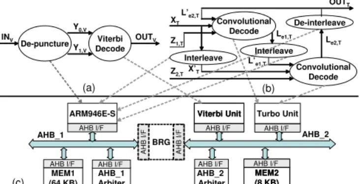
XT Z1,T Z2,T Le1,T L’e1,T Le2,T L’e2,T OUTT MEM1 (64 KB) AHB I/F ARM946E-S AHB I/F Viterbi Unit AHB I/F Viterbi Unit AHB I/F Turbo Unit AHB I/F BRG AHB_2 Arbiter AHB I/F MEM2 (8 KB) AHB I/F MEM2 (8 KB) AHB I/F AHB_1 AHB_2 (c)
AHB I/F AHB I/F
AHB_1 Arbiter AHB I/F OUTV (a) (b) INV Y0,V Y1,V X’T De-puncture Viterbi Decode De-interleave Interleave Interleave Convolutional Decode Convolutional Decode
Fig. 1. Integrated Viterbi-Turbo decoder design: functional specification of (a) Viterbi decoder, (b) Turbo decoder, and (c) mapping of functional blocks to integrated decoder architecture
The rest of this paper is organized as follows. In Sec-tion II, we present illustrative examples that motivate our work. In Section III, we describe the proposed adaptation methodology. In Section IV, we describe the required hard-ware support and how the platform is adapted at run-time. In Section V, we present experimental results that evaluate the application of the proposed approach to the design of an integrated Viterbi-Turbo decoder.
II. MOTIVATION
In this section, we illustrate, using an integrated IEEE 802.11a Viterbi and UMTS Turbo decoder design, the advantages of an integrated approach to dynamic data re-location and bus reconfiguration.
A. Case Study: Integrated Viterbi-Turbo Decoder Design
Viterbi coding is a popular channel coding technique used in a wide variety of wireless standards [12]. Figure 1(a) illustrates the tasks that constitute Viterbi decoding [13]. The noise-contaminated received bits, INV, are first “de-punctured” by inserting dummy zero values in place of the bits that were “punctured” at the transmitter (puncturing is a process of omitting some encoded bits to increase the coding rate). The Viterbi decode task then generates the output decoded bits, OU TV. Turbo coding is another popular channel coding technique used in third-generation cellular standards [14]. Figure 1(b) shows the tasks involved in Turbo decoding [13]. The decoder receives the noise-contaminated bits,XT,Z1,T andZ2,T. Turbo decoding op-erates in an iterative manner (Figure 1(b)), such that outputs of the first convolutional decoding task are interleaved and input to an identical second convolutional decoding task, whose outputs are in turn de-interleaved and input back to the first decoding task. After a number of such iterations (typically 8 for low bit error rate), a hard (0 or 1) decision about the value of each bit is output (OU TT).
The integrated Viterbi-Turbo decoder design is motivated by the emergence of converged handsets that are capable of operating over multiple air interfaces simultaneously [15]. The data rate requirements for Viterbi and Turbo decoding may vary over time depending on application data rate, signal strength, number of users, etc. Figure 1(c) shows the mapping of the Viterbi and Turbo tasks to a set of hardware components and software running on an embedded processor (ARM946E-S). The Viterbi and Turbo decoding block sizes are set to 1024 bits. The bus architecture is based on the AMBA AHB bus standard [16] and consists
TABLE I
VITERBI ANDTURBO DECODING DATA OBJECTS
XT Soft Input Systematic bits 1024 bytes
X’T Interleaved Systematic bits1024 bytes
Z1,T Soft Input Parity bits 1 1024 bytes
Z2,T Soft Input Parity bits 2 1024 bytes
Le1,T LLR1 bits 1024 bytes L’e1,T Interleaved LLR1 bits 1024 bytes Le2,T LLR2 bits 1024 bytes L’e2,T De-interleaved LLR2 bits 1024 bytes Data
Objects Purpose Size
INV Soft Input bits 1536 bytes Y0,V De-punctured bits 1 1024 bytes Y1,V De-punctured bits 2 1024 bytes OUTV Decoded Output bits 512 bytes
STableV State History bits 5120 bytes
App.
Viterbi
Turbo
OUTT Decoded Output bits 512 bytes
of two bus segments connected by a two-way bridge. The platform also has two SRAM memory components, MEM1 and MEM2, connected to the bus segments. Table I shows the different data objects used by the Viterbi and Turbo applications, and their sizes.
The Viterbi-Turbo decoder was optimized using the in-tegrated adaptation techniques proposed in this paper. The design features two dynamic configurability options: (i) dynamic relocation of the Viterbi and Turbo data objects between MEM1 and MEM2, and (ii) dynamic bus topology reconfiguration through dynamic bridge by-pass [17], a technique that enables the internal logic of the bridge to be “by-passed” at run-time, thereby merging the two bus segments into a single shared bus. In the following exam-ples, we analyze the performance of the resulting design under illustrative scenarios.
Example 1:We first consider an application scenario where
only the Viterbi decoder is executing. Table II shows the maximum data rates achieved under different combinations of data placement and bus configuration. We observe that, under a single shared bus (i.e., when the bridge is by-passed), all data placements give the same performance, since both MEM1 and MEM2 are on the same bus. However, under a multiple bus architecture, data placement 1 shown in Table II achieves the highest data rate. This shows that the optimal placement of data in memory depends on the underlying bus topology. Also, if data placement 1 is used, the multiple bus architecture results in the highest data rate, while if data placement 4 is used, the single shared bus architecture gives a higher data rate. This shows that for best performance, bus topology selection should take into account the placement of data in memory.
The above example illustrates that the placement of data in memory and the bus configuration are interdependent, and
TABLE II
VITERBI DECODING DATA RATES UNDER DIFFERENT DATA PLACEMENT AND BUS CONFIGURATIONS
Data Placement
INV
Single Shared Bus Multiple Bus Bus Topology 30.1591 Mbps 30.1591 Mbps 30.1591 Mbps 30.1591 Mbps 52.4926 Mbps 46.3901 Mbps 40.7515 Mbps 9.9071 Mbps INV, OUTV, Y0,V INV, OUTV, Y0,V, Y1,V INV, OUTV, Y0,V, Y1,V, STableV MEM1 MEM2 Y0,V, Y1,V, STableV, OUTV Y1,V, STableV STableV -# 1. 2. 3. 4.
0 10 20 30 40 50 0 1 2
Turbo Data Rate (Mbps)
Viterbi Data Rate (Mbps)
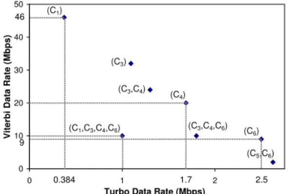
(C1) (C3) (C3,C4) (C 4) (C1,C3,C4,C6) (C3,C4,C6) (C 6) (C5,C6) 46 0.384 1.7 2.5 9
Fig. 2. Viterbi and Turbo decoding data rate requirements and platform configurations that can satisfy them
should be jointly optimized. We next make the case for this joint optimization to be performed dynamically.
Example 2: Consider the simultaneous execution of both
Viterbi and Turbo decoders. Figure 2 illustrates the Viterbi and Turbo decoding “data rate space”. Each point in this space consists of a specific data rate requirement for Turbo decoding and concurrent Viterbi decoding. For some sample points in the data rate space, Figure 2 shows different data placement and bus architecture configurations (see Table III in Section V-B) under which they are achievable. For ex-ample, when the data rate requirement is1M bps,10M bps for Turbo and Viterbi decoding, respectively, multiple plat-form configurations (C1, C3, C4 and C6) can satisfy it. However,onlyconfigurationC1can satisfy the requirement
of 384Kbps,46M bps, while only configuration C4 can
satisfy the requirement of 1.7M bps,20M bps. Configu-rations C1 and C4 differ in the way data is placed in memory (Table III). We also observe that when the decoding requirement is 2.5M bps,9M bps, only configuration C6, which employs a single shared bus, can satisfy it. Finally, if the application requirements change at run-time from
384Kbps,46M bpsto1.7M bps,20M bps, the only way
to satisfy both requirements is to dynamically change the configuration from C1 toC4.
The above example illustrates that dynamic data relocation and bus reconfiguration enable the design to achievea larger performance space. This is because data relocation enables the placement of data in memory to be optimized to best suit the current requirements of the executing applications, while adapting the bus configuration enables it to be better matched to the resulting on-chip communication traffic profile.
In summary, the above examples motivate the need for integrated, dynamic adaptation of the on-chip communica-tion and memory architectures. We next describe a platform adaptation methodology based on such an approach.
III. PLATFORMADAPTATIONMETHODOLOGY
In this section, we first describe the problem of run-time platform adaptation, and present an overview of our methodology to address it. We then describe the key steps of the methodology in detail.
A. Problem Description and Methodology Overview
We consider a partitioned and mapped SoC platform architecture whose components are connected to a set of bus segments interconnected by bridges. The platform executes
a set of applications, A1, A2, ..., AN, with corresponding time-varying data rate requirements, DR1, DR2, ..., DRN. The platform is enhanced to support the relocation of application data objects in memory, and reconfiguration of the bus architecture through by-pass of some or all of the bridges. The problem of platform adaptation is to select the optimized placement of the application data objects in memory, and the bus configuration (i.e., which bridges are to be by-passed) at run-time, such that the performance requirements of all the applications can be satisfied.
Adaptive Platform Architecture Applications Typical
Input Stimuli
Relocatable Data Object Sizes, # Accesses
2. Generate all platform configurations
3. Select candidate configurations
4. Characterize data rate space achievable per candidate configuration
5. Partition data rate space
Platform Configuration Table Candidate configurations Relocatable Data Objects 1. Application profiling
Fig. 3. Dynamic data relocation and bus configuration methodology Figure 3 shows our overall platform adaptation method-ology. Each application Ai is associated with a set of relocatable data objects Di = {di,1, di,2, ..., di,M}. For each di,j, we first determine its size si,j, and estimate the average number of accesses ni,j,k to it from each platform component Pk, through simulation using typical input stimuli (step 1). We then generate an exhaustive list of all possible platform configurations Cl = Mm, Bn, where Mm represents the data placement configuration, and Bn the bus configuration (step 2). This configuration space is then pruned to a subset of candidate platform configurations, such that each can potentially cover a unique region of the application data rate space (step 3). Next, each candidate configuration is analyzed to estimate the set of points in the data rate space that it can achieve (step
4). Finally, the application data rate space is partitioned among the candidate configurations (step 5). The result of the methodology is a Platform Configuration Table that lists, for each data rate partition, the associated optimized platform configuration. This table is used to perform run-time platform adaptation (described in Section IV). We next describe the highlighted steps in the methodology in detail.
B. Methodology Details
Selection of Candidate Configurations: To select the
candidate configurations, for each applicationAi, under each platform configuration Mm, Bn, we compute the total number of “cross-bridge” accesses (i.e., accesses across a bridge) Ti,m,n, to the application’s relocatable data objects Di. This is given byTi,m,n=
M
j=1
Pkni,j,k×BRGi,j,k,
where BRGi,j,k is the number of intermediate bridges
between component Pk, and data object di,j, and depends on the platform configuration. Next, for each configuration
Mm, Bn, the total number of cross-bridge accessesTi,m,n, for each applicationAi, are compared to the corresponding number of cross-bridge accesses Ti,r,n, under all other data placement configurations Mr, but for the same bus configuration Bn. If there exists a configuration for which Ti,r,n ≤Ti,m,n for all applications, then the configuration Mm, Bn is discarded; otherwise, it is chosen as a candi-date configuration. This is based on the hypothesis that for a given bus configuration, data placements that result in a larger number of cross-bridge accesses are inferior to those that result in fewer cross-bridge accesses. Note that, we do not prune configurations across different bus configurations at this stage since it would require a detailed control flow analysis of the applications, as the bus configuration affects the system concurrency.
Characterization of Data Rate Space Achievable under
each Candidate Configuration: Next, we determine the
data rate space achievable under each candidate config-uration (Figure 3). Exact characterization of this space would require exhaustive performance analysis of the system under all possible combinations of application data rate requirements because it depends on the fine-grained control flow and data access profile of the individual applications. Clearly, this would be infeasible for most systems. However, the objective of this step is to enable a good partitioning of the overall application data rate space (step 5 in Figure 3), for which even a coarse-grained approximation of the data rate space under each candidate configuration is sufficient. Therefore, we propose a technique to approximate this data rate space based on a limited number of detailed simulations.
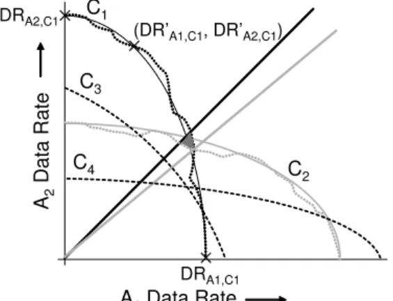
A1Data Rate C1 × A2 D a ta Rate C2 DRA1,C1 DRA2,C1 (DR’A1,C1, DR’A2,C1) × × C3 C4
Fig. 4. Data rate space characterization and partitioning for two applica-tions
To illustrate this, let us consider an example system exe-cuting two applicationsA1andA2. Figure 4 shows the exact data rate space achieved under a candidate configurationC1 (the region between the dark dotted curve and the axes). To approximate this curve, the platform is simulated under configuration C1 using typical input stimuli for (i) each application executing alone, resulting in points (DRA1,C1,0)
and (0,DRA2,C1), and (ii) with both applications executing
concurrently processing as fast as possible, resulting in point (DRA1,C1, DRA2,C1) in Figure 4. Next, we use a quadratic parametric spline curve fitted to these three points, resulting in the dark solid curve for C1. For the points on the Y-axis and X-Y-axis, the parameter value is set to 0 and 1, respectively, while for the third point it is set tody/(dx+dy), wheredxanddyare the Euclidean distance of the third point
from the point on the X-axis and Y-axis, respectively. In our experiments, we found that such curves can approximate the actual data rate space well. Note that, more accurate characterization can be performed using more simulations of the platform, resulting in a larger number of points to fit the curve. Other performance analysis techniques [8], [9] can also be used in this step to speedup simulation.
The above procedure is repeated for all candidate config-urations, to characterize their respective data rate spaces.
Partitioning of the Data Rate Space: Finally, the
over-all application data rate space is partitioned among the candidate configurations, such that in each partition, the associated platform configuration is best able to satisfy the applications’ data rate requirements. To illustrate this, we consider another candidate platform configuration C2, for the above example system. Figure 4 shows the exact (light dotted curve) and our approximated (light solid curve) data rate space achieved under C2. The line joining the intersection of the approximated curves for C1 andC2, and the origin (dark solid line) partitions the data rate space, such that for points that lie above this line,C1is preferable, while for those below this line, C2 is preferable. Figure 4 also shows the ideal partitioning of the data rate space derived based on the exact data rate curves (light solid line). The shaded area in the figure indicates the data rate region that cannot be achieved due to the inaccuracy introduced by our approximation. The size of this region is system dependent. In our experiments, this size was found to be quite small, as shown in the results.
Figure 4 also shows the estimated data rate space under two other candidate configurations C3 and C4 (dashed curves). Redundant configurations such as C3 should be pruned, since their data rate space is completely subsumed by other configurations, while configurations such as C4 should not, as they can achieve a unique region of the data rate space. Therefore, the methodology partitions the data rate space only among configurations whose individual data rate spaces form the envelope of the total achieved data rate space (in this case, C1, C2 and C4). This is performed as follows. We start with the candidate con-figuration Ci, whose data rate curve intersects the Y-axis at the highest point. The intersection points of this curve with the curves under all other candidate configurations,
Ii = {(XCi,C1, YCi,C1),(XCi,C2, YCi,C2), ...}, are then
computed. The first chosen intersection point is one with the highest Y value, say (XCi,Cj, YCi,Cj), and this forms the first partition of the data rate space with the associated configuration being Ci. Next, the intersection points of the curve for Cj with those for the other configurations is computed. The intersection point selected among them is the one with the highest Y value less than YCi,Cj, and this forms the second partition with Cj as the associated configuration. This process is continued until no more intersection points can be selected. These partitions and the associated configurations form the Platform Configuration Table, which is used for run-time platform adaptation as described in the next section.
Extension to an Arbitrary Number of Applications:
For each candidate configuration, the system is simulated for all possible combinations of the applications executing together, thus requiring C∗(2|N|−1) simulations for N
applications and C candidate configurations. In practice, we expect N to be fairly small. The data rate space under each configuration is then approximated by fitting these data rate points to an N-dimensional surface. The application data rate space is then partitioned among the configurations whose individual data rate spaces form the envelope, by determining the intersection of their data rate spaces, as in the two application case.
IV. RUN-TIMEPLATFORMADAPTATION
In this section, we first describe the hardware support re-quired for enabling data relocation and bus reconfiguration, and then describe how the platform is adapted at run-time.
A. Hardware Support
Relocation of data is performed using direct memory access (DMA) and an optimized bus configuration. The overhead of data relocation depends on the relocated data size, memory access times, bus characteristics (e.g., burst modes), and bus speeds. After relocating a data object, all future references to it must find it at its new location. For references from processors, this is ensured by changing the virtual to physical address mapping of the relocated data in the processor’s page table. For references from platform hardware components, “base-plus-offset” addressing modes must be used for each relocatable data object. On data relo-cation, the corresponding base pointer values are updated to point to the new base address. Since data relocation is handled differently for processors and other hardware components, an integral number of pages should be allocated to relocatable data objects which are accessed by both.
To enable dynamic reconfiguration of the bus topology, the inputs to the bridge’s master and slave interfaces are routed to the outputs, using multiplexers to optionally by-pass the bridge. When multiple bus segments are merged together, only one bus master can be granted access to the resulting shared bus at any given time. This is ensured by using a distributed bus arbitration protocol, in which the arbiters of the different bus segments co-operatively gener-ate grants. A Bus Reconfiguration Unit is responsible for generating the control signals to by-pass different bridges. The exact penalty of bus reconfiguration depends on the number of pending bus transactions, but has been previously shown to be on the order of a few tens of bus cycles [17].
B. Platform Adaptation
The platform adaptation method is illustrated in Figure 5. This functionality is implemented as low-level firmware routines executing on the embedded processor(s) in the platform. Applications communicate changes in their data rate requirements through an API (application programming interface). The run-time firmware searches the Platform Configuration Table using the new and existing data rate requirements to identify the current point in the data rate space and the pre-computed optimized data placement and bus configuration. Data is relocated by by-passing all the necessary bridges, and then using DMA mode of transfer. Next, the base pointer registers and processor page-tables are updated. Finally, the Bus Reconfiguration Unit is instructed to by-pass selected bridges according to the identified plat-form configuration. API Change in application data rate? No Yes
Search PC-table for current point in DR space Data rates of concurrent applications Platform Configuration Table By-pass bridges Transfer data by DMA Current
configuration
Configure Bus Architecture
System with relocated data
System with reconfigured bus & relocated data
Platform Configuration
Update base pointers Update page table
Fig. 5. Run-time Platform Adaptation V. EXPERIMENTALRESULTS
In this section, we present experimental results that eval-uate the performance benefits of applying the proposed methodology to the integrated Viterbi-Turbo decoder design.
A. Experimental Methodology
The integrated Viterbi-Turbo decoder design was imple-mented using an instruction set model for the ARM proces-sor, and programmable VERA bus-functional models [18] for the Viterbi Unit, Turbo Unit, and the memories. The configurable bus architecture with bridge by-pass was imple-mented by enhancing a reference RT-level implementation of the AMBA AHB bus [18], using the techniques described in [17]. The design was operated at a frequency of 400 MHz. Performance results were obtained through simulation with ModelSim [19].
B. Application to the Viterbi-Turbo Decoder Design TABLE III
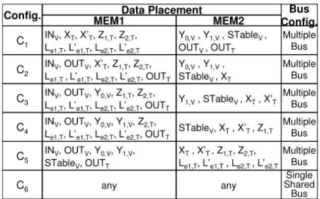
CANDIDATE DATA PLACEMENT AND BUS CONFIGURATIONS
Y0,V, Y1,V, STableV , OUTV , OUTT
INV, OUTV, Y0,V, Z1,T, Z2,T, Le1,T, L’e1,T, Le2,T, L’e2,T, OUTT INV, OUTV, Y0,V, Y1,V, Z2,T, Le1,T, L’e1,T, Le2,T, L’e2,T, OUTT INV, OUTV, Y0,V, Y1,V, STableV, OUTT
Data Placement Bus
Config. Multiple Bus Multiple Bus Multiple Bus Multiple Bus any Single Shared Bus Config. C1 C3 C4 C5 C6 MEM1 MEM2 INV, XT, X’T, Z1,T, Z2,T, Le1,T, L’e1,T, Le2,T, L’e2,T
Y1,V, STableV , XT, X’T STableV, XT, X’T , Z1,T XT, X’T , Z1,T, Z2,T, Le1,T, L’e1,T, Le2,T , L’e2,T
any Y0,V, Y1,V, STableV , XT Multiple Bus C2 INV, OUTV, X’T, Z1,T, Z2,T, Le1,T , L’e1,T, Le2,T, L’e2,T, OUTT
The proposed methodology was applied to the integrated Viterbi-Turbo decoder design. The total number of possible platform configurations was 7422, which our methodology pruned to only 6 candidate configurations (Table III). The size of the data rate space that cannot be achieved due to the inaccuracy introduced by our approximation was found to be less than2%of the total data rate space that can be achieved (estimated using detailed simulation of all configurations). Table IV shows the resulting Platform Configuration Table for the design. The candidate configurationsC2andC5were redundant, and hence, do not appear in the table.
TABLE IV
PLATFORMCONFIGURATIONTABLE
DRV≥40.8 DRT DRV<21.46 DRT & DRV≥8.03 DRT DRV<8.03 DRT Data Rate Requirement DRV<40.8 DRT & DRV≥21.46 DRT Configuration C1 C3 C4 C6
C. Platform Adaptation Overhead
The worst case overhead for data relocation (to copy data, and update page tables and base pointers) was observed while switching between configurations C1 and C4, and
was measured to be approximately 10 µs (using a DMA
unit, with single cycle memory access, and with the bridge by-passed). The average bus reconfiguration overhead (to enable or disable bridge by-pass) was measured to be approximately 10 cycles. This shows that the platform adap-tation overhead is negligible compared to the granularity at which the data rate requirements are expected to change (tens of milliseconds [20] or higher).
D. Impact of Platform Adaptation on Performance
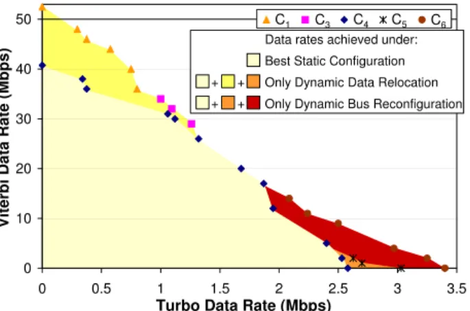
Figure 6 shows the data rate space achieved under joint data relocation and bus reconfiguration for the design (com-plete shaded area). It also shows the platform configurations selected for each data rate combination simulated (only points on the outer edge of the complete shaded region). To evaluate the performance improvements achieved through our scheme we compared it to the performance achieved under three other cases: (i) the best static configuration, which is C4, as it can satisfy the largest space of data rates among all candidate configurations; (ii) only dynamic data relocation, while keeping the bus configuration fixed as a multiple bus; (iii) only dynamic bus reconfiguration, while keeping the data placement fixed as in the best static configuration. From the figure, we observe that joint data relocation and bus reconfiguration can satisfy a much larger space of data rate requirements compared to a statically configured design (e.g., up to 32% data rate improvements when only Turbo decoding executes). We also observe that by exploiting both data relocation and bus reconfiguration together, the space of data rates achieved is much larger than when they are individually configured.
0 10 20 30 40 50 0 0.5 1 1.5 2 2.5 3 3.5
Turbo Data Rate (Mbps)
Viterbi Data Rate (Mbps)
C1 C3 C4 C5 C6
Data rates achieved under: Best Static Configuration Only Dynamic Data Relocation Only Dynamic Bus Reconfiguration + +
+ +
C1 C3 C4 C5 C6
Fig. 6. Data rate space achieved under different platform adaptation schemes
VI. CONCLUSIONS
In this paper, we studied adaptive SoC platforms featur-ing two different dynamic configurability options, namely,
data relocation and bus reconfiguration. We illustrated the interdependence between these features, and presented a methodology for their co-ordinated run-time adaptation. Ex-periments on an integrated 802.11a Viterbi and UMTS Turbo decoder design indicate that the proposed methodology results in significant performance improvements compared to conventional statically optimized platform architectures.
REFERENCES
[1] B. Xu and D. H. Albonesi, “Runtime reconfiguration techniques for efficient general-purpose computation,”IEEE Design and Test of
Computers, vol. 17, pp. 42–52, Mar. 2000.
[2] K. Sekar, K. Lahiri, and S. Dey, “Dynamic platform management for configurable platform based System-on-Chips,” inProc. Int. Conf.
Computer-Aided Design, pp. 641–648, Nov. 2003.
[3] R. Ho, K. W. Mai, and M. A. Horowitz, “The future of wires,”Proc. IEEE, vol. 89, pp. 490–504, Apr. 2001.
[4] P. R. Panda, N. D. Dutt, A. Nicolau, F. Catthoor, A. Vandecappelle, E. Brockmeyer, C. Kulkarni, and E. D. Greef, “Data memory organi-zation and optimiorgani-zation in application-specific systems,”IEEE Design
& Test Magazine, vol. 18, pp. 56–68, May 2001.
[5] K.Lahiri, A.Raghunathan, and S.Dey, “Design of high-performance system-on-chips using communication architecture tuners,” IEEE
Trans. Computer-Aided Design, vol. 23, no. 6, pp. 919–932, 2004.
[6] S. Pasricha, N. Dutt, and M. Ben-Romdhane, “Fast exploration of bus-based on-chip communication architectures,” inProc. Int. Conf.
Hardware/Software Codesign and System Synthesis, pp. 242–247,
Sept. 2004.
[7] R. Banakar, S. Steinke, B. S. Lee, M. Balakrishnan, and P. Marwedel, “Scratchpad memory: Design alternative for cache on-chip memory in embedded systems,” inProc. Int. Symp. on HW/SW Codesign, pp. 73– 78, May 2002.
[8] P. Grun, N. Dutt, and A. Nicolau, “Memory system connectivity exploration,” in Proc. Design Automation & Test Europe (DATE)
Conf., pp. 894–901, Mar. 2002.
[9] A. Papanikolau, K. Koppenberger, M.Miranda, and F. Cathoor, “Memory communication network exploration for distributed low power memory organizations,” inProc. IEEE Workshop Signal
Pro-cessing Systems, pp. 176–181, 2004.
[10] P. Knudsen and J. Madsen, “Integrating communication protocol selection with hardware/software codesign,”IEEE Trans.
Computer-Aided Design, vol. 18, pp. 1077–1095, Aug. 1999.
[11] P. Marchal, F. Catthoor, D. Bruni, L. Benini, J. Gomez, and L. Pinuel, “Integrated task scheduling and data assignment for SDRAMs in dynamic applications,” IEEE Design & Test Magazine, vol. 21, pp. 378–387, Sept. 2004.
[12] “Part 11: Wireless LAN Medium Access Control (MAC) and Physical Layer (PHY) specifications.” IEEE Std 802.11a-1999
http://standards.ieee.org/getieee802/download/ 802.11a-1999.pdf.
[13] B. Vucetic and J. Yuan, Turbo Codes: Principles and Applications. Kluwer Academic Publishers, Norwell, MA, 2000.
[14] “Universal Mobile Telecommunications Systems (UMTS); Multiplex-ing and channel codMultiplex-ing (FDD).” 3GPP TS 25.212 version 3.4.0 Re-lease 1999 http://www.3gpp.org/ftp/Specs/archive/ 25_series/25.212/25212-340.zip.
[15] “Philips debuts reference design for converged handsets.”
http://www.eet.com/news/latest/showArticle. jhtml?articleID=159402638, Mar. 2005.
[16] “AMBA 2.0 specification.”http://www.arm.com/products/ solutions/AMBA_Spec.html.
[17] K. Sekar, K. Lahiri, A. Raghunathan, and S. Dey, “FLEXBUS: A high-performance system-on-chip communication architecture with a dynamically configurable topology,” in Proc. Design Automation
Conf., pp. 571–574, June 2005.
[18] “Synopsys DesignWare Intellectual Property.” http://www. synopsys.com/products/designware/designware. html.
[19] “Modelsim 5.7e.”http://www.model.com.
[20] A. Aguiar and J. Klaue, “Bi-directional WLAN channel measure-ments in different mobility scenarios,” in Proc. IEEE Vehicular