Worcester Polytechnic Institute
Digital WPI
Major Qualifying Projects (All Years) Major Qualifying Projects
April 2015
Wireless Biomedical Signal Chain
Long Hoang Nguyen
Worcester Polytechnic Institute
Lou Abigail Seneres
Worcester Polytechnic Institute
Neda Seyedmahmoud
Worcester Polytechnic Institute
Robert Michael Perry
Worcester Polytechnic Institute
Follow this and additional works at:https://digitalcommons.wpi.edu/mqp-all
This Unrestricted is brought to you for free and open access by the Major Qualifying Projects at Digital WPI. It has been accepted for inclusion in
Major Qualifying Projects (All Years) by an authorized administrator of Digital WPI. For more information, please [email protected].
Repository Citation
Nguyen, L. H., Seneres, L. A., Seyedmahmoud, N., & Perry, R. M. (2015).Wireless Biomedical Signal Chain. Retrieved from
Analog Integrated Circuit Applications
by
Long Nguyen, Robert Perry, Lou Seneres, Neda Seyedmahmoud
Submitted to the Faculty of the
Worcester Polytechnic Institute
In partial fulfillment of the requirements for the
Degree of Bachelor of Science in
Electrical and Computer Engineering
Long Nguyen
Robert Perry
Lou Seneres
Neda Seyedmahmoud
Professor John McNeill
MQP Advisor
This report represents the work of WPI undergraduate students submitted to
the faculty as evidence of completion of a degree requirement. WPI routinely
publishes these reports on its website without editorial or peer review. For
more information about the projects program at WPI, please see
Abstract
The goal of this project is to design an ultra-low power and ultra-portable wireless biomedical signal chain. This project provides an adaptable electrocardiogram (ECG) reference design that can be modified to accept other bio-potential signals. The designed ECG monitoring system utilizes the AD8232 from Analog Devices featuring low noise and adaptable filtering as well as the nRF51422 for Bluetooth Low Energy (BLE) signal transmission. The resulting design addresses the lack of commercial products that can transmit a conditioned signal over-the-air by providing an adaptable reference design that others can utilize to expedite research and development.
Acknowledgements
The completion of our project would not be accomplished without the sponsorship of the New England Center for Analog and Mixed Signal Integrated Circuit Design (NECAMSID) lab.
We would like to thank the following individuals for their contributions: • Michael Coln from Analog Devices Inc
• David Plourde from Analog Devices Inc • Ina Duka from Analog Devices Inc • Bob Boisse at WPI ECE Shop
Finally, we would like to extend our sincerest thanks to our Major Qualifying Project advisor, Professor John McNeill for his patience, constant support, and guidance throughout this project.
Contents
1 Introduction . . . 1
1.1 Problem Statement . . . 1
1.2 Project Definition . . . 2
1.2.1 Analog Front End . . . 2
1.2.2 Communications . . . 2
1.2.3 Power . . . 3
1.2.4 User Interface . . . 3
2 Analog Front End . . . 4
2.1 Background Research . . . 4
2.1.1 Monitoring ECG - Electrode Location and Waveform Quality . . . . 4
2.2 AFE Requirements . . . 7 2.3 Design Options . . . 8 2.3.1 Instrumentation Amplifier . . . 8 2.3.2 Specialty Chips . . . 10 2.4 Design Decision . . . 14 2.5 Design . . . 15 2.6 Testing Capabilities . . . 16 2.7 Adaptability . . . 17
2.8 Primary testing and evaluation . . . 17
2.8.1 ECG Waveform . . . 18
2.8.2 Transfer Function . . . 20
2.8.3 Frequency Response . . . 20
2.8.4 Step Response . . . 24
2.8.5 Switch and Jumper Settings . . . 26
2.8.6 Supply Current . . . 30
2.8.7 ECG Signal 2-electrode Issues . . . 31
3 Communications . . . 34
3.1 Background Research . . . 34
3.1.1 Bluetooth Low Energy Protocol . . . 35
3.1.2 TI CC2540 Keyfob . . . 37 3.2 nRF51-DK . . . 39 3.2.1 Hardware . . . 39 3.2.2 Software . . . 40 4 Power . . . 43 4.1 Background Research . . . 43 4.1.1 Storage Elements . . . 43
4.2 Preliminary Design Options . . . 46
4.2.1 TI CC2541 Measurements . . . 47
4.3 Testing Evaluation . . . 49
4.3.2 Power Consumption Analysis . . . 50
4.4 Design Decisions . . . 58
4.4.1 Maximizing Battery Capacity . . . 60
4.4.2 Parallel Capacitor Calculation . . . 60
4.4.3 Improving Battery Life . . . 61
5 User Interface . . . 65 5.1 Background Research . . . 65 5.1.1 Mobile Platforms . . . 65 5.1.2 App Builder . . . 66 5.1.3 Existing Applications . . . 68 5.1.4 Decision . . . 69 5.2 Development . . . 69 5.2.1 Structure . . . 69 5.2.2 Functionality . . . 70 5.2.3 Alternative solutions . . . 71 6 System Design . . . 72 6.1 First Revision . . . 74 6.2 Final Revision . . . 76 6.3 Specification Overview . . . 78
7 Design Testing and Results . . . 81
7.1 First Revision . . . 81
7.2 Final Revision . . . 89
8 Future Works . . . 90
9 Conclusion . . . 92
10 Appendices . . . 97
10.1 AFE First Revision Schematic . . . 124
10.2 AFE Second Revision Schematic . . . 125
10.3 Communication Block First Revision Schematic . . . 126
10.4 Communication Block Second Revision Schematic . . . 127
10.5 PCB Prints . . . 128
10.5.1 First Revision Top View . . . 128
10.5.2 First Revision Bottom View . . . 129
10.5.3 Second Revision Top View . . . 130
List of Figures
1.1 System Level Block Diagram . . . 2
2.1 Einthoven’s Triangle [1] . . . 4
2.2 Lead Location and ECG Output [2] . . . 5
2.3 2-electrode Location Options . . . 6
2.4 3-electrode Best Setup . . . 6
2.5 2-electrode Location Options . . . 7
2.6 2-electrode Best Setup . . . 7
2.7 The Classic 3 Op-amp In-amp Circuit [3] . . . 8
2.8 Simplified Schematic of AD8236 [4] . . . 9
2.9 AD8236 Heart Rate Monitor Reference Configuration [4] . . . 10
2.10 ADAS1000 Functional Block Diagram [5] . . . 11
2.11 Functional Block Diagram[6] . . . 13
2.12 AD8232-EVALZ Board[7] . . . 17
2.13 Evaluation Board Setup . . . 18
2.14 Three Electrodes Configuration Lead I . . . 19
2.15 Three Electrodes Configuration Lead II . . . 19
2.16 Two Electrode Configuration - Oscilloscope Capture . . . 20
2.17 Frequency Response Test Setup . . . 21
2.18 Frequency Response measurement circuit diagram . . . 22
2.19 Frequency Response Comparison . . . 24
2.20 Step Response . . . 25
2.21 Zero Pole Plot . . . 26
2.22 FR disabled (left) and FR enabled (right) . . . 27
2.23 Faster Restore Circuit AD8232 [Analog Devices] . . . 28
2.24 AC Leads off Detection . . . 29
2.25 Shutdown Current vs. Temperature (System Performance) . . . 29
2.26 Operation enabled (left) and Shutdown mode (right) . . . 30
2.27 Measuring Current Supply with Series Resistor . . . 30
2.28 Supply Current vs. Temperature (System Performance) . . . 31
2.29 Normal 2-electrode configuration with less noise . . . 32
2.30 When touching a laptop battery source When touching metal underneath desk 32 2.31 When touching metal above desk When touching on the desk . . . 33
3.1 Connection Diagram . . . 36
3.2 BLE Error Checking on TX and RX . . . 37
3.3 CC2541 Keyfob [8] . . . 37
3.4 CC2540 Dongle [9] . . . 38
3.5 Test Pins Schematic . . . 38
3.6 nRF51422 Block Diagram . . . 39
3.7 nRF51422 Built-in ADC [10] . . . 40
3.8 nRF51422 Embedded Softdevice [10] . . . 41
3.9 nRF51422 Alert Notification Timing while using the S110 Softdevice [11] . . 42
3.10 nRF51422 Alert Notification Timing while using the S110 Softdevice [11] . . 42
4.2 Method of Constant Voltage then Constant Voltage Charging [13] . . . 45
4.3 ADP5061 . . . 46
4.4 Preliminary Block Diagram Power Analysis . . . 47
4.5 Timing Diagram . . . 47
4.6 TI CC2541 Current Testing Setup [14] . . . 48
4.7 Current Consumption vs Time during a single Connection Event [14] . . . . 48
4.8 Current Measurement for TI CC2541 Connection Event . . . 49
4.9 Revised Block Diagram Power Analysis . . . 49
4.10 Current Measurement Setup for nRF51 [15] . . . 50
4.11 Calculated data for Energy Consumption vs. Number of Bits . . . 53
4.12 Measured Data for Energy Consumption vs. Number of Packets . . . 54
4.13 Energy Consumption vs. ADC sampling rate . . . 56
4.14 Nordic Current Waveforms (Advertising and Connection Event) . . . 57
4.15 Nordic Current Waveforms Multi-packet . . . 57
4.16 CR2032 Coin Cell Continuous Discharge [16] . . . 59
4.17 Peak Current Magnitude impact with 25ms pulse cycle on CR2032 Battery Capacity [16] . . . 60
4.18 Proposed circuit for battery life improvement . . . 61
4.19 Battery Parallel Capacitor Circuit . . . 62
4.20 Transient Analysis (pulse load w/parallel capacitor circuit) . . . 63
4.21 Current plot for load, battery, and capacitor respectively . . . 64
5.1 Flow Chart . . . 70
5.2 Functions of the main screen . . . 71
6.1 Final System Block Diagram . . . 72
6.2 AFE Filter Configuration [17] . . . 72
6.3 nRF51422 Pinout . . . 73
6.4 nRF51422 Embedded Program Flow Diagram . . . 74
6.5 System Blocks First Revision . . . 75
6.6 Stack Up Layers . . . 76
6.7 Second PCB Board Top View . . . 77
6.8 Second Revision Stack Up Layers . . . 78
6.9 Second PCB Board Layout Front View . . . 78
6.10 Second PCB Board Layout Bottom View . . . 79
6.11 System Block Diagram . . . 79
6.12 CR1632 Coin Cell Pulse Drain Characteristics [18] . . . 80
7.1 AFE Verification Setup . . . 81
7.2 First Revision AFE Verification from Function Generator . . . 82
7.3 First Revision AFE Verification from Real Human Signal . . . 82
7.4 Device RAM mapping . . . 83
7.5 Loading Service . . . 83
7.6 Communications Current Measurement Setup . . . 84
7.7 Current Consumption during BLE Connection . . . 84
7.8 First Revision Current Consumption during Connection Event . . . 85
7.9 First Revision Current Consumption during Advertising Event . . . 85
7.11 Using the manufacturer’s Android app . . . 87 7.12 Test drive with Adafruit BLE-Friend custom services . . . 88 7.13 The Python Graphing with HRM firmware . . . 89
List of Tables
1.1 Decision Matrix for Possible Project Ideas . . . 1
2.1 AFE Decision Matrix . . . 14
2.2 Frequency Response Derivation . . . 23
2.4 Frequency Response Derivation . . . 26
2.6 Frequency Response Derivation . . . 27
3.1 Communications Protocol . . . 34
4.1 Secondary Battery Cell Characteristics . . . 44
4.2 Energy Harvesting Techniques [19] . . . 46
4.3 Energy Consumption with 1-packet at ˜10ms connection interval . . . 52
4.4 Energy Consumption with 6-packet at 100ms connection interval . . . 52
4.5 Energy Consumption with Varying Packet Size at ADC sampling rate of 60Hz 54 4.6 Average time on with varying Packet size at ADC rate of ∼ 15Hz . . . 55
4.7 Energy Consumption Depending on the ADC sampling rate . . . 55
4.8 CR2032 Specifications [20] . . . 58
4.9 Final Voltage vs. Capacitor Value . . . 62
5.1 Mobile Platforms Comparison . . . 66
6.1 Coin Cell CR1632 Specifications . . . 80
1
Introduction
The initial purpose of this project was to investigate and define an application for an inte-grated circuit from Analog Devices Incorporated (ADI). Analog Devices provided information regarding a capacitive application [21], but it was concluded that the depth of that particu-lar application would be more indicative of a graduate thesis than an undergraduate Major Qualifying Project (MQP). Therefore, the project transformed from a single application into a broad range of applications with the use of Analog Devices chip in the final design. At the direction of our advisor Professor McNeill, the team began to generate ideas related to biomedical applications. These preliminary ideas can be seen in Table 1.1.
Table 1.1: Decision Matrix for Possible Project Ideas
Idea Feasibility Uniqueness Presentability Complexity Cost Average
Portable ECG Sensor 8 8 8 6 7 7.4
Biovisualization 5 5 1 7 10 5.6
Pulse or Blood Flow Sensor 8 2 8 3 3 4.8
Traffic Flow Sensor 2 3 0 6 10 4.2
The ideas in Table 1.1 were rated in several categories such as feasibility, uniqueness, pre-sentability, complexity, and cost on a scale of 1 to 10 with 1 being favorable and 0 being most unfavorable. For example, a 0 in the feasibility category would mean that the design is not feasible. Complexity is rated from 0 to 10 with 10 being the most favorable for design complexity.
1.1
Problem Statement
Based on the 2008 data by American Heart Association (AHA), an average of more than 2150 Americans die of Cardiovascular Disease (CVD) each day, or average of 1 death every 40 seconds. The cost of CVD is estimated to be 320 billion USD in 2011 [22]. According to this data the CVD requires extra attention and monitoring. This project addresses this problem by designing an electrocardiogram (ECG) monitoring device.
The widespread usage of health monitoring devices in the United States has increased the demand for smart portable health monitoring systems. Depending on the application of the systems, portable biomedical monitoring devices for temperature, blood pressure and glucose level measurements are commonly used and are widely available to the users. Commercially available wireless portable biomedical acquisition and transmission devices for measuring ECG signal are limited. This project attempts to create a reference design for untethered and portable ECG device and user interface that can be modified for other signals.
1.2
Project Definition
The goal of this project is to design an ultra low power, and ultra portable system. The project started with a desired system that includes five blocks: Power, Analog Front End (AFE), Microcontroller, Communications, and User Interface (UI) as shown in Figure 1.1. The project topic and specifications were chosen after a research and brainstorming phase. After this stage, the group decided upon designing a wireless biomedical application system that matches the design requirements. The design is mainly concerned with ECG measure-ments. However, it can be expanded to measure other small biopotential signals. The ECG was chosen for the purpose of this project because it is feasible and easy to measure with simple snap electrodes on hands or the chest.
AFE ADC Microcontroller Communications User Interface
Figure 1.1: System Level Block Diagram
Figure 1.1 illustrates the system level, or rather very general, potential modules for the project. These were group according to functionality into four main modules such as Analog Front End, Communications (which is composed of the ADC, Microcontroller, and Wireless Communications Protocol), Power, and User Interface. Each section will be briefly described and analyzed in the next subsections.
1.2.1 Analog Front End
When it comes to biomedical signals, signal integrity and precise measurements are necessary components to ensure the accuracy of monitoring and diagnosis. The purpose of this block is to amplify and filter ECG signal to eliminate the motion artifacts. The amplitude of ECG ranges from 0.1mV to 1mV and its bandwidth is from 0.2Hz to 200Hz, therefore the AFE must have the capability to reject the common-mode noise [23]. Given the small signal for the ECG, an amplifier can be utilized to amplify the low signal without adding appreciable noise. Also, appropriate low pass filters can be used to remove the unwanted high frequency noise signals if necessary.
1.2.2 Communications
The communication block of the design is responsible for transmitting the acquired ECG raw signal to the user interface for monitoring and diagnosis. Other functionality of this block includes data conversion and processing. The ECG amplitude is small therefore, the analog to digital conversion before transferring can be done using a Successive Approximation (SAR) ADC of 10 to 12 bits precision. The communication method chosen for the desired portable system is untethered, in order to provide a user friendly experience for the end users. The
ECG monitoring signal needs to remain close to the body with wireless communication that would make it more feasible to connect to different user interfaces without changing the hardware configuration of the system.
1.2.3 Power
Due to the low power and portability restraints of the system design, quantifying the system power is of particular importance. The system should maximize battery life, while attempting to minimize size of the storage medium. In addition to maintaining a low power ECG monitoring system, the system power block must fulfill the basic safety, lifetime, portability and the size consideration of the desired system. It is desirable for the runtime to be sufficiently long such that the user does not need to worry about changing the battery except throughout the week. However, if this is not possible, an indicator to charge or replace the battery should be in place to give the user ample time to change the battery. This project explores the usage of either a primary or secondary cell depending upon the current draw of the design as a lifetime of more than a few days. These properties will be investigated further in Chapter 4.
1.2.4 User Interface
The user interface need to be easy-to-use. It shall also allow for direct and continuous observation of ECG results collected from the other blocks. For the purposes of this project, a desktop or smartphone application can be utilized to demonstrate the ECG signal due to its increasing popularity and availability. Different mobile platforms and other alternatives will be considered for user interface.
2
Analog Front End
Bio-potentials are very weak signals compared to environmental noise sources and Analog-to-Digital Converters (ADC) are not able to process such small signals. Therefore, for proper signal acquisition, a system generally requires an Analog Front-End (AFE) to condition the acquired signal. This project focuses on ECG signal acquisition, so the AFE block is an important requirement for the designed system. The AFE block must be easy to integrate within the system and specifically with the system’s ADC. The ECG signal is also susceptible to noise interference and motion artifacts. As a result, the signal conditioning must include the extraction, gain and filtering stages. The purpose of this chapter is to provide information regarding AFE block of the system and its specifications.
2.1
Background Research
2.1.1 Monitoring ECG - Electrode Location and Waveform Quality
In order to have a better understanding of the ECG monitoring systems, a background research was done on the electrode location and ECG waveform quality. ECG system has two or more electrodes used to monitor voltage across one or more leads. Clinical standard uses a 12-lead ECG that would each provide a view of the heart’s electrical activity from different views. Each lead corresponds to a vector of ECG electrical potential. The electrodes are typically placed in a setup known as the Einthoven’s triangle, which is formed by the right arm (RA), left arm (LA) and left leg (LL) sensing electrodes as shown in Figure 2.1 below. These are the basis for the frontal axis.
Different lead location corresponds to different ECG signal as shown in Figure 2.2 below. Lead II is commonly used as it provides largest positive R-wave that is important to measure heart rate.
Figure 2.2: Lead Location and ECG Output [2]
Three-electrode Configuration
This configuration would allow a Lead I, Lead II or Lead III to be selected. The two electrodes are used to form a vector while the third electrode is the reference. For three electrodes, it is possible to have up to three unique vectors. This implementation has the advantage having less noise and more lead selection options.
The first option would require three electrodes located around the heart. It has views of Lead I, II and III. One disadvantage is the ease of use as it might have to cross over pectoral muscles and breast tissue. Another alternative aims to provide better comfort for the patient. The trade-off would limited lead view as it only has a good view of Lead II. The two options are shown in Figure 2.5.
Figure 2.3: 2-electrode Location Options
In this case, a desired setup is shown in Figure 2.4. This would provide better view of Lead II. The right-leg drive (RLD) electrode (usually a third electrode) is used to bias the patient to a set DC operating point in order to ensure that the input at the same potential as the monitoring system.
Figure 2.4: 3-electrode Best Setup
Two-electrode Configuration
In this configuration, only one lead is possible. To obtain a Lead II vector, the configuration is shown in Figure 2.5 for option one. Another alternative setup, option two, is also possible but it only has a good view of Lead I. This setup is desired since it is easier for patient.
Figure 2.5: 2-electrode Location Options
In this case, an ideal setup is shown in Figure 2.6. This would provide better view of Lead I. One disadvantage is a smaller amplitude of the signal compared to Lead II in three-electrode configuration.
Figure 2.6: 2-electrode Best Setup
2.2
AFE Requirements
The AFE block of an ECG monitoring device must extract low voltage signals ranging from
0.1−1mV with frequency range of 0.2−200Hz [23]. The signal extraction is critical in the presence of noisy conditions and various interferences. The designed system is preferred to have the capability to use both two and three-electrode configurations. In ECG mea-surements, skin electrode contact counts as a source of interference producing an offset of ±200−300mV.
Two type of signals are available at the input of the AFE block, the Common-Mode (same potential) and Differential-Mode (different potential) signals. For ECG signal monitoring applications, the Common-Mode signal is highly undesirable. The potential between the electrodes and ground can create a Common-Mode component of up to 1.5V [3]. One
differential signal at the input pins. The Common-Mode gain is defined as the ratio of change in output voltage to change in Common-Mode input voltage. The Common-Mode Rejection Ratio (CMRR) is the ratio of the differential gain to the Common-Mode gain. The desired AFE must have a CMRR of 80dB to 120dB over the input frequencies that need to be rejected [3].
In order to achieve gain as well as Common-Mode rejection, instrumentation amplifier (in-amp) can be employed. An instrumentation amplifier has a differential input and single-ended output with respect to a reference voltage. The in-amp gain is determined by external resistors that are connected between inverting input and the output [3]. Figure 2.7 shows the internal structure of a classic in-amp with 3 operational amplifiers (op-amps).
Figure 2.7: The Classic 3 Op-amp In-amp Circuit [3]
2.3
Design Options
This project stipulates that products from Analog Devices are preferred over their competi-tors’ offerings. Analog Devices offers different solutions ranging from general to application-specific chips. After evaluating Analog Device’s portfolio of integrated circuits, three design options were considered. These options include two application-specific ICs and a lower power general purpose instrumentation amplifier.
2.3.1 Instrumentation Amplifier AD8236
Among the instrumentation amplifiers available in the market, the AD8236 has the lowest power consumption [4]. It can operate on a single supply of 1.8V or 3V. Other features of AD8236 are high input impedance, minimum gain of 5, low input bias of 1pA and high CMRR of 110dB. The AD8236 is a monolithic (on a single base semiconductor, referred to as a die) amplifier. In addition to above features, its rail-to-rail input and output provides a wide dynamic range, which means that its maximum input or output swing is equal to
the power supply voltage [3]. The AD8236 REF pin shown in Figure 2.8 allows for shifting the output according to the application. This shifting makes it easier for the AFE block to interface with other blocks of the system such as the ADC. According to its specification, the AD8236 has configurable gain with default value of 5; by placing a resistor across the RG pin, additional gain can be set with respect to the resistor value. The resistor value can be calculated according to Equation 2.1.
RG =
420kΩ
G−5 (2.1)
All of the pins of the AD8236 are protected against Electrostatic Discharge (ESD) as shown in the simplified schematic Figure 2.8.
Figure 2.8: Simplified Schematic of AD8236 [4]
The AD8236 has DC overload protection, which allows a diode drop (approximately 0.7V) above the positive supply and a diode drop below the negative supply. It also can handle a continuous 6mA current. The AD8236 has relatively high CMRR (110dB) and the capabil-ity to remove any differential DC offsets resulted from electrode half-cell potential. These features make AD8236 a good candidate for ECG monitoring applications. The suggested configuration of AD8236 is shown in Figure 2.9.
Figure 2.9: AD8236 Heart Rate Monitor Reference Configuration [4]
2.3.2 Specialty Chips ADAS1000
Purpose
The ADAS1000 is a high-performance, low power analog front end (AFE) IC. This chip ensures the quality of the signal and allows for monitor and diagnostics of ECG signal. It follows the various standards for diagnostic electrocardiograph devices. In addition to measuring the ECG, this chip can measure thoracic impedance and pacing artifacts[5]. The capability of measuring pace artifacts allows for detection of presence of a pacemaker and its effects [24]. Thoracic impedance measurements or the respiration measurement can also be used for monitoring patient breathing. The functional block diagram of the ADAS1000 is shown in Figure 2.10.
Figure 2.10: ADAS1000 Functional Block Diagram [5]
Input
The ADAS1000 has five input channels and a reference drive, Right Leg Drive (RLD) for ECG signal acquisition. The channels include a differential preamplifier with a programmable gain, a fixed gain 2-pole anti-aliasing filter, a 14 bit 2MHz SAR ADC, and buffers. The implemented anti-aliasing filter is aimed for pace detection. Leads can be configured as either digital and analog.
The RLD amplifier is used to reject the noise and interference and adjust internal reference level and provide maximum input dynamic range[5].
Power Consumption
The ADAS1000 is designed to run off a battery or a standard power line. The chip required supply voltage of 3.3V to 5V. The power consumption ranges from 11mW for one-lead to 15mW for three-leads, and 21mW if all the electrodes are in use. The ADAS1000 has a feature for scaling between noise and power, meaning that the noise can be reduced by increasing the power consumption whenever necessary. It also features power-down mode where the signal acquisition channel can be shut down and the data rates can be reduced to minimize power consumption[5].
Additional Features
The ADAS1000 offers the capability of AC and DC lead off detection. The reference lead can be selected according to the application. It includes externally supplied crystal of (8.192M Hz) and internal regulators.
A self-test mode is implemented to ensure proper operation of the integrated circuit. The power up testing of the ADAS1000 performs registers reading, Cyclic Redundancy Check (CRC) and calibration of the Digital to Analog Converter (DAC).
Post processing of the aquired data can be performed on a DSP or microcontroller through Serial interface SPI as well as QSPI and DSP. The ADAS1000 transmits the data at pro-grammable data rates either in the form of a data frame supplying either lead or electrode data[5].
AD8232 Purpose
The AD8232 is designed for ultra-low power applications and has the capability to acquire, amplify and filter bio-potential signals. This chip is capable of eliminating the motion arti-facts and the electrode half-cell potential. It also features leads off detection circuitry and fast restore ability to prevent a long recovery time resulted from input disconnection. The functional block diagram of the AD8232 is shown in Figure 2.11 indicating that the chip includes four amplifier an in-amp (IA), an operational amplifier (op-amp) A1, a Right Leg Drive (RLD) A2, and a buffer amplifier A3.
Figure 2.11: Functional Block Diagram[6]
Input
Two-electrode and three-electrode configurations are possible using the AD8232. In the three-electrode configuration, the Right Leg Drive (RLD) can be used as the reference lead. The Right Leg Drive amplifier is employed for rejecting the Common-Mode voltage of the system at the input of the instrumentation amplifier (CMRR = 86dB). The terminals of the AD8232 are protected against electrostatic discharge (ESD). External resistors can be utilized to avoid overload conditions at the input[6].
Gain and Signal Conditioning
The AD8232 includes an in-amp with a fixed gain of 100. It also features an op-amp for creating low pass filter with selectable cutoff frequency for additional noise removal. To avoid Radio Frequency Interference (RFI) and as a result DC offset at the output, a low pass filter with cutoff frequency of 1.1M Hz is implemented at each input pins of the AD8232 [6].
Additional Features
The reference buffer is used to create a virtual ground (reference voltage) between the actual ground and the supply. This reference voltage can be driven from REFIN pin using a voltage divider and an external voltage source. The virtual ground is available at REFOUT for use in the circuitry.
The AD8232 provides AC and DC leads off detection. The three electrode configuration uses DC lead off detection in which each input terminal is checked for connection. In this case if the IN+ electrode is disconnected the LOD+ pin is set and if the IN- is disconnected the LOD- pin set.
AC lead off detection is used for two-electrode configuration. This is done by injecting a small current into the input terminals. This feature informs the user with disconnection of either electrodes but it does not specify which electrode is disconnected[6].
Power Consumption
The AD8232 operates on a single supply such as CR2032 cell batteries or rechargeable lithium ion batteries. To reduce the power consumption, the chip provides a shutdown mode with the current draw of less than 200nA[6].
2.4
Design Decision
Comparing the three AFE blocks from the analog devices, all options were rated base on the complexity, portability and adaptability. The ADAS1000 offers more features but is more complex and requires more power. The AD8236 is a general purpose instrumentation amplifier and requires additional signal conditioning components (at least four op-amps Figure 2.9) to meet the project’s needs. This may increase the AFE block footprint. The AD8232, however, has less complexity and power consumption compared to ADAS1000. Conversely, it offers more features than AD8236. Therefore, AD8232 was evaluated to be the best fit for the purposes of this project. Table 2.1 shows a quantitative decision matrix, indicating that ADAS1000 has the highest power consumption and AD8236 does not include the desired features.
Table 2.1: AFE Decision Matrix
IC CMMR* Supply Voltage Supply Current Number of Electrodes ADC Precision
[dB] [V] [µA] [bit]
ADAS1000 110 3.15-5.5 785 5 14
AD8232 86 2-3.5 170 3 N/A
AD8236 110 1.8-5.5 33 N/A N/A
2.5
Design
AD8232 was chosen for AFE block in the designed system since it has the capability to accommodate both the two-electrode and three-electrode configurations. The values of re-sistances in the device are all chosen to have large values in order to minimize the power consumption[7]. Adaptability is the key feature of the design. As shown in the schematic In Appendix 10.1, several components have the value of Do Not Install (DNI). This is to allow for additional filtering or amplification. The user can chose the value of DNI capacitors and resistors to match their desired configuration for different applications.
The two electrode configuration use LA and RA pins as an input, whereas the three-electrode configuration uses right leg drive (RLD) pin in addition to RL and LA. Fast restore func-tionality is enabled by setting the corresponding pin (FR) to high to achieve a better signal quality. The default leads off detection features is set to AC for two-electrode configuration but can be adapted for three-electrode configuration (DC) as well. The pins corresponding to the AC and DC leads off detection LO+ and LO- interface to the communication block for further processing and informing the user. The 10MΩ resistors R7, R8 are input bias resistors. These input resistances must be biased for the in-amp to function properly for two-electrode configuration. Three solder jumpers (SJs) available on the design make it possible to bias these resistors with correct voltage values. For two-electrode configuration, connecting SJ3 pads biases the resistors with RLD voltage value while SJ2 uses the REFOUT voltage for biasing. Resistors R9 and R10 are chosen as 182kΩ.
The output of the AFE block is fed to the input of communication block ADC for data conversion and transition. To reduce the power consumption, SDN mode pin interfaces to communication block of the system and can be controlled digitally. This allows reducing the current drawn as necessary to reduce the power consumption[7].
As it is shown in the schematic in Figure 10.1 R11 and R12 are forming a voltage divider system connected to supply voltage +VS. This divider creates a midsupply voltage level at REFIN. According to the architecture of the device using a buffer amplifier, the same voltage level appears at the pin REFOUT. C17 is used for filtering the power line noise[7]. C13 and C12 are DC coupling capacitors. The output signal is filtered and amplified by a two-pole Sallen Key low-pass filter. R17, R18, C21 and C25 are responsible for this filtering. The Equations 2.2 and 2.3 are used to calculate the cut-off frequency and gain of the two-pole Sallen Key low-pass filter, and are taken from AD8232 data sheet[6].
fc= 1 2π·√R17·R18·C21·C25 = 1 2π·√200kΩ·1MΩ·10nF ·22nF = 23.99Hz (2.2) Gain= 1 +R20 R23 = 1 + 1MΩ 100kΩ = 11 (2.3)
the cutoff frequency of the high-pass filter is given by Equation 2.4. fc= 100 2π·R5·C13 = 100 2π·10MΩ·0.22µF = 7.23Hz (2.4)
The gain of 11 multiplies to the fix gain of 100 from in-amp which brings the total gain of the AD8232 to 1100.
A7.23Hzcutoff frequency allows for the in-amp to reject the DC components of the inputs[7]. C22 and R22 create an AC coupling network between the output of the in-amp output (IAOUT) and the REFOUT pin. This allows for negative signal swing as well as creates a second pole at the location of 7.23Hz for the highpass filter. The highpass filter at the output of in-amp has total of 40dB decrease in magnitude response per decade[7].
fc=
1
2π·R22·C22 =
1
2π·100KΩ·0.22µF = 7.23Hz (2.5)
The capacitor C20 located between the RLD and RLDFB pins is chosen to be 1nF. The placement of C20 is to improve the CMRR at the inputs of the in-amp when three electrode configuration is used. The C20 and 150kΩ resistor of the Right Leg Drive Amplifier form an integrator and gain of 20 at 50Hz to60Hz. The output current of the Right Leg Drive opposes the variations of the Common-Mode voltage. To maintain a stable system, R16 is chosen to be 499kΩ. R16 also limits the current flowing to the RLD pin of AD8232 to be less than 10µAfor safety reasons[7].
2.6
Testing Capabilities
As shown in the design schematic, a total number of 10 test points are implemented. The test points allow for observing the input or output of each stage or pin. TP1 and TP2 are intended for current drawn measurements across the R2. R2 with the resistance of 10Ω is installed between the battery and the +VS of the AD8232. This provides testing capability and power calculation by measuring the current drawn by the AD8232 in various modes. TP3, TP4 and TP5 correspond to AD8232 input channels (electrodes) to which the input signal can be connected. TP6 is connected to the OUT pin of the AD8232. TP6 and ground can be used to monitor the output of the AFE block. If low pass filters are applied to the output of AD8232, TP7 (one-pole low pass filter), TP8 (two-pole low pass filter) and TP10 (three-pole low pass filter) can be used to test the output of the AFE block. TP10 is for measuring the REFOUT voltage. The REFOUT voltage in the current configuration of the design must equal to half of the voltage supply.
2.7
Adaptability
This project requires the design to be flexible and adaptable to other monitoring situations. Consequently, pads for extra passive components are included in the design to allow for future options. Installing the resistors R19 and R21 results in additional low pass filtering of the output. The RC systems to be used for this purpose are (R19 and C26) and (R21 and C24). C24 and C26 has a value of 1uF. The reference voltage REFOUT can also be filtered using R24 and C27 system. C27 is installed as 1uF while the R24 is not populated. R15 can be used to limit the loop gain of the RLD amplifier and shift its dominant pole[7]. The capacitors C14, C15 and C16 are not populated but they can be installed for additional Radio Frequency Interference (RFI) filtering. RFI filters can be used for improving the CMRR when C15 and C16 are the same value. This yields common-mode signal cutoff frequency given by Equation 2.6.
fc=
1
2π·R14·C15 (2.6)
The next step was to perform primary testing of AFE block which will be described in the next subsection.
2.8
Primary testing and evaluation
For evaluation and reference purposes of the AD8232, the evaluation board (AD8232-EVALZ) as shown in Figure 2.12 was used. In order to have a better understanding of the AD8232 and be able to evaluate its functionality, some of the AD8232-EVALZ datasheet analysis was replicated.
2.8.1 ECG Waveform
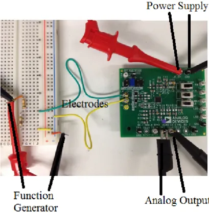
For reliable heart signal from the AD8232 evaluation board, electrode connections were soldered properly. The setup used is shown in Figure 2.13. Scope was connected to OUT and GND with input bias set by power supply P3. In the 3-electrode configuration, the output signal is show in the next few figures. Different electrode locations were used to test which location has best good view of the heart signal and provides most amplitude.
Figure 2.13: Evaluation Board Setup
The output in the Figure 2.14 shows the ECG signal with Lead I configuration. The output signal is about 1V peak to peak.
Figure 2.14: Three Electrodes Configuration Lead I
When the electrodes are placed so as to provide good view of Lead II, the output signal shown in the Figure 2.15 appears to be more amplified with a peak to peak of almost 1.5V.
Figure 2.15: Three Electrodes Configuration Lead II
Two electrode configuration provided the ECG output in Figure 2.16. The peak to peak value is 500mV which is generally small.
Figure 2.16: Two Electrode Configuration - Oscilloscope Capture
2.8.2 Transfer Function
Based on the frequency response, the transfer function was derived to have of a two-pole low pass filter (constitutes as zeros) and a two-pole high-pass filter (constitutes as poles). Based on the filter configuration there are four poles having two real and two complex poles and two zeros with complex zeros with cutoff frequency at 15Hz or 95 rad/sec. The transfer function was determined to be:
H(s) = (s 2+s+ 20) s 95 + 1 2 ( 95s2+ 2∗0.6∗ s 95 + 1) 2.8.3 Frequency Response
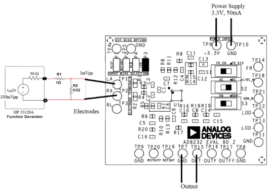
The next step was to use the evaluation board and be able to achieve correct frequency response using the data sheet as a reference. The AD8232-evalz evaluation board was setup by connecting the power supply common to GND terminal and a 3.3V supply voltage at the +3.3V terminal. The left arm (LA) terminal and the right arm (RA) terminal are connected to the signal source. For this evaluation, an arbitrary ECG signal from function generator was used. The output signal is available on the OUT terminal.
The set-up used to perform measurements is shown in Figure 2.17. The function generator was set to "High Z" as it has factory impedance set to 50Ω since high impedance gives less distortion on waveform.
Figure 2.17: Frequency Response Test Setup
For testing, the frequency range gathered was from 1Hz to 1000Hz. A voltage divider was used to provide a 1mV pp input to accommodate a low ECG signal from the function generator. Input bias REFOUT at P2 was used.
Figure 2.18: Frequency Response measurement circuit diagram
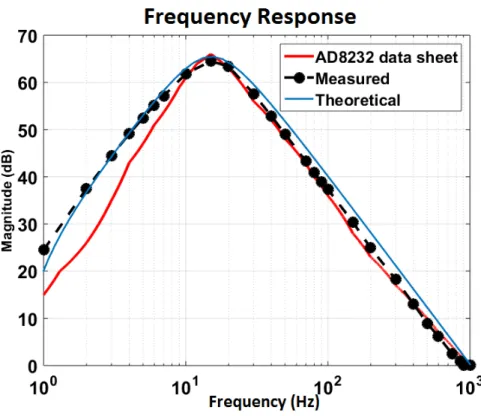
The transfer function of the signal from the differential input of the in-amp to OUT with the default filter configuration is shown in Figure 2.19.
Table 2.2: Frequency Response Derivation Frequency Amplitude [Vpp] Gain Gain [db]
[Hz] Vin [V] Vout [V] Vout/Vin
1 0.0100 0.1680 17 2 0.0100 0.7440 74 3 0.0100 1.6600 166 4 0.0100 2.8600 286 5 0.0050 2.1000 420 6 0.0050 2.8600 572 7 0.0040 2.8800 720 10 0.0020 2.4600 1230 15 0.0020 3.3600 1680 20 0.0020 2.9600 1480 30 0.0020 1.5200 760 40 0.0020 0.8800 440 50 0.0020 0.5680 284 70 0.0050 0.7280 146 80 0.0050 0.5560 111 90 0.0050 0.4400 88 100 0.0050 0.3680 74 150 0.0050 0.1650 33 200 0.0100 0.1760 18 300 0.0100 0.0816 8 400 0.0100 0.0450 5 500 0.0100 0.0280 3 600 0.0150 0.0304 2 750 0.0150 0.0199 1 850 0.0150 0.0168 1 900 0.0150 0.0152 1 1000 0.0150 0.0150 1
In Figure 2.19, a comparison between the theoretical frequency responses based from the evaluation board data sheet with the interpolation, the measured data, and the derived transfer function are provided.
Figure 2.19: Frequency Response Comparison
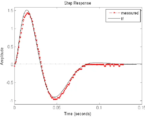
2.8.4 Step Response
For the step response, the transfer function was scaled to have an amplitude value similar to the measured data. This was found by calculating the ratio between the derived transfer function amplitude and the measured data, which is found to be 0.0019. As shown in Figure 2.20, the derived transfer function is comparable to the measured data.
Figure 2.20: Step Response
Zero-pole analysis is shown in Figure 2.21. The imaginary part is on the x-axis while real part is the y-axis. There are two complex zeros and two finite pole located at z= -95. There are two complex poles located at about ±95j where j is the imaginary unit.
Output of step response produces the above figure. The overshoot is due to the zeros of low pass filter and the poles of high-pass filter. Second order filter causes resonance especially for complex poles. The zero-pole map diagram is shown in Figure 2.21.
Figure 2.21: Zero Pole Plot
2.8.5 Switch and Jumper Settings
Another feature for AD8232 is the switch settings for that could be configurable for either a 2-electrode or 3-electrode capability. Different modes of AD8323 were investigated as shown in Table 2.4.
Table 2.4: Frequency Response Derivation
Label Options Setting
S1 FR_EN / FR_DIS Fast restore enabled
S2 AC / DC Leads off detection
S3 EN / SDN Operation enabled/ shutdown
Fast Restore
This mode reduces the duration of long settling tails of the high-pass filters that allows the AD8232 to recover quickly and therefor to take valid measurements soon after reconnecting
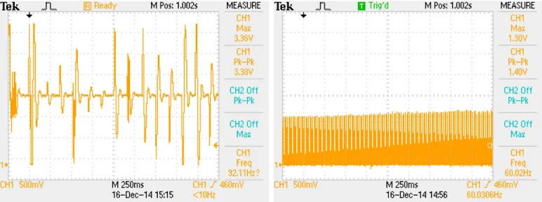
the electrodes. To enable, switch S1 is set to FR_EN position.
The configuration used was a frequency input of 1Hz with1mV pp, source3.3V and max cur-rent limit to 0.5A. When FR is disabled, the restore time is t=1.980s. When FR is enabled, the restore time is significantly faster with t=0.240s. Moreover, as shown in Table 2.22, when two leads are off, the restore time if enabled is slower than when only one lead is off.
Table 2.6: Frequency Response Derivation
Setting FR_DIS Restore time [s] FR_EN Restore time [s]
LA lead off (one electrode) 1.980 0.240
Both leads off (two electrodes) 1.840 1.020
RA lead off (one electrode) 1.980 0.380
Figure 2.22: FR disabled (left) and FR enabled (right)
These values can be compared to AD8232 plots as shown in Figure 2.23. When only one electrode is disconnected, it has an average recovery time of 0.25s when FR is enabled. The recovery time when it is disabled is approximately 2 seconds.
Figure 2.23: Faster Restore Circuit AD8232 [Analog Devices]
Leads off detection
The leads off detection feature provides modes optimized for either two-electrode or three-electrode configuration of the device. The AC leads off detection is used for two-three-electrode setup. To maintain the inputs inside common-mode range of the amplifier, the bias level for the inputs can be set to REFOUT or RLD by placing the jumper at P2 or P4. The AD8232 detects when an electrode is disconnected by sourcing a small 100kHz current into the electrodes.
The DC leads off detection is used for three-electrode setup that works by sensing when either input goes high. The RLD output terminal must be connected to a driven electrode. It can detect which electrode is disconnected through pins LOD+ and LOD-.
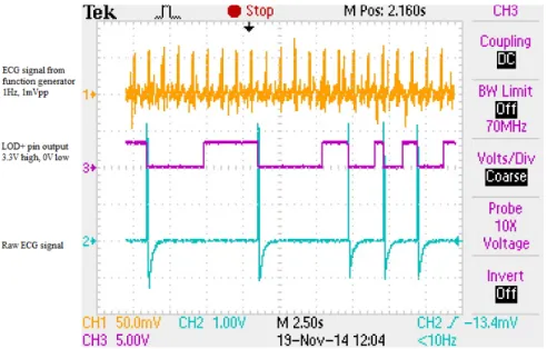
When the leads off detection S2 is set to AC, the output at LOD+ pin produces a high digital value that would indicate that an electrode is disconnected. For testing the AC-lead off detection feature, a sample ECG signal was used from the function generator with 1Hz
and 1mV pp. Output is shown in Figure 2.24 where the middle graph is the LOD+ pin
Figure 2.24: AC Leads off Detection
For two-lead electrode configuration, the LOD+ pin has a high or low output. When one electrode is disconnected, the LOD+ pin signals a high value (3.3V) and when the electrode is connected again, it goes to a low value (0V). Initially, the pin has a low output signal.
Operation Enabled/Shutdown
According to AD8232 system specifications shown in Figure 2.25, shutdown current has typical values depending on temperature and the voltage supply.
To verify this operation, current was measured during shutdown mode by finding the voltage drop at output when connected to a series resistor of 1MΩ. It was measured with the following values for input from the function generator: 1Hz, 1mVpp. The resistor value was measured for accuracy and found to be R = 0.976kΩ. Equation 2.7 was used to find shutdown current usage and was verified from Figure 2.25.
I = VDROP
R =
72mV
0.976 kΩ = 73.77 nA (2.7)
When shutdown pin is high, the output signal produces a small sinusoidal voltage as shown in Figure 2.26.
Figure 2.26: Operation enabled (left) and Shutdown mode (right)
2.8.6 Supply Current
According to AD8232 Data sheet, current value is typically170µA. The current supply usage was measured and found to be 166µA with a power supply set to 3.3V and 50mA current limit. Current was found by measuring voltage drop across resistor then performing Ohm’s law as shown in Equation 2.8. Current measurement setup is shown in Figure 2.27.
Figure 2.27: Measuring Current Supply with Series Resistor
I= VDROP
R =
0.183 mV
This value is comparable to the Supply Current vs. Temperature plot from the AD8232 data sheet shown in Figure 2.28. At room temperature, the expected supply current is approximately 170µA.
Figure 2.28: Supply Current vs. Temperature (System Performance)
2.8.7 ECG Signal 2-electrode Issues
After conducting preliminary testing, the functionality and features of AD8232 were verified. Results show that two-electrode configuration is more susceptible to AC noise. It was also found that the ideal ECG location would use Lead I which is typically a smaller signal. That is, the device is designed so that it will easily be snapped onto a person’s chest as shown in Figure 2.29 which also shows a typical 2-electrode configuration with less noise and laptop and other devices in vicinity. To find which sources would produce the most AC noise, different test setups were used such as touching materials in the vicinity. It was found that when touching a laptop battery source or the metal underneath the desk, 2-electrode signal is vulnerable to noise as shown in Figure 2.30. Otherwise, when the metal above desk or on the desk was touched, it was able to produce results as shown in Figure 2.31.
Figure 2.29: Normal 2-electrode configuration with less noise
3
Communications
3.1
Background Research
The communications block has several requirements that must be met in order for total system integration.
Requirements
• Ability to run off a 2-3V supply • Less than 20 mA peak current draw • Minimize Complexity
• Easy integration with mobile devices
Based on the requirement for low power operation, the Bluetooth Protocol was chosen for further evaluation as it allows for potential integration with mobile devices by using the built-in Bluetooth radio that most mobile devices and laptops contain. Moreover, it is lower current consumption than standard Bluetooth or Bluetooth Enhanced Data Rate (EDR), which typically consumes a excess of 100mA, which would result in a very low battery discharge time.
Table 3.1: Communications Protocol
Protocol Frequency Power Device Integration ADC
XBee/ZigBee 950 MHz/2.4 GHz Medium No No
RF Mesh Networks No standard Low No No
BLE/ANT 2.4 GHz Low Yes Yes
Wi-Fi 2.4 GHz High Yes No
Untethered communication is a fundamental requirement for this project. Therefore, the communication block of the design is responsible for wireless transmission of data to the user interface. Since this project is targeting a low power application, communication block with low power consumption is preferred. Another requirement would be the capability to easily integrate with the smartphones. Among the existing protocols, Wi-Fi and Bluetooth, capability are integrated within the smartphones. This will eliminate the need of an inter-mediate transceiver module. The communication block must also be battery operated with supply voltage of 2V to 3V.
Both Wi-Fi (IEEE 802.11 standards) and Bluetooth operate in2.45GHz band. Conversely, these two protocol have completely different data transmission rates. Higher data rate would
require more power consumption. This project is concerned with monitoring application. Bio-potential monitoring applications do not require high data transmission rate compared to data streaming applications such as playing music or video. Therefore, high data trans-mission rate is not a requirement for the desired design. Among the available wireless com-munication protocols, Bluetooth v4.0 or Bluetooth Low Energy (BLE) (also called Bluetooth Smart) has the lowest data transmission rate of 0.3M bps.
3.1.1 Bluetooth Low Energy Protocol
Bluetooth devices are divided into three categories depending on their mode of operation such as dual mode, single mode and Bluetooth classic-only devices. Dual mode devices sup-port both Bluetooth classic and Bluetooth low energy (BLE). Single mode (Smart Devices) devices only support the BLE while classic-only devices are intended for classic Bluetooth protocol. BLE uses a different standard than classic Bluetooth that is mainly designed for monitoring cell battery operated applications[25]. BLE transmits data at a lower data rate with respect to classic Bluetooth. Therefore, it is more energy efficient.
Devices with BLE capabilities are restricted to transmission of packets of data with maxi-mum of 20 bytes. This is to reduce the energy cost of recalibration for each transmission. Bluetooth architecture includes three main layers such as controller, host, and application. The Controller is the Bluetooth module. The host contains protocols and procedures. The Characteristic is a Universal Unique ID (UUID) which is a machine-readable specification. The Application includes characteristic, service, and profile. The Service is the human-readable specification of set of characteristics. The Profile describes devices with services on them and specifies how they need to be connected or discovered[25].
Evaluating the BLE solutions available in the market, this project only considers the system-on-chip (SoC) modules. This decision was made to eliminate the need of an external micro-controller and external ADC. This was done to reduce the complexity of the project while benefiting from an integrated design options. This section investigates the capabilities of Texas Instruments (TI) CC2540 and Nordic Semiconductors nRF51422.
Connection
Figure 3.1: Connection Diagram
Initially, it is in the advertising or initializing state and then it moves into the connected state in both circumstances. After the timeout period is reached or a specified sleep time, the device enters standby mode. The scanning mode is entirely separate from the rest of the operations as it is just data and not necessary for connection if a BLE device address is known.
Error Detection and Correction
According to the Bluetooth Core Specification v4.0, the stack must be able to detect and mitigate errors. Therefore, the stack implements cyclic redundancy checking (CRC) on both the transmitter and the receiver radios. Although this takes processor time and adds to current consumption, it also adds to reliability. The TX and RX CRC checks are shown in the flow diagram Figure 3.2.
Figure 3.2: BLE Error Checking on TX and RX
3.1.2 TI CC2540 Keyfob
Based on the requirements, the Texas Instrument CC2541-DK Keyfob Figure 3.3 for the communication block was chosen. This board comes with a supporting dongle CC2540 Figure 3.4. These boards are programmable by IAR Embedded Workbench Software for 8051 processors. Moreover, the CC2541 utilizes Hardware Abstraction Layer (HAL) that eliminates the need for low level programming.
Figure 3.4: CC2540 Dongle [9]
The ADC of CC2541 supported up to 14-bit analog-to-digital conversion with 12 bits Effec-tive Number of Bits (ENOB). It included eight individually configurable channels (differential or single ended) and a reference voltage generator. Single-ended inputs from the ADC are accessible through virtual channels 0 to 7 corresponding to physical pins 0 to 7 of port 0 on the chip. In this configuration, channels 6 and 7 are chosen as the ADC input. The pin configuration is shown in Figure 3.5.
Figure 3.5: Test Pins Schematic
Performing the initial testing of the CC2541, the value read by the ADC did not change with the varied input voltage. Same test was performed on the CC2540 however, for testing purposes such as power measurements the CC2540 is not favorable. Therefore alternative solutions were considered to proceed with the design. These solutions include using an exter-nal ADC or use of the ADC on CC2540 Dongle and then send the data over to the CC2541. Both of these options defeated the requirements set in the beginning. Another constraints regrading using the CC2541 was the cost of the SDK. The SDK required to program the CC2541 provides a free license for 30 days. The team negotiated with the company and got an extended free license for 60 more days however, it was decided that the licence restriction would not allow enough time to modify the firmware in future. Therefore another design options for communication block was considered. The alternative BLE solution considered was nRF551422 [10]. This chip is an ARM Cortex M0 based so it has a free SDK. Moreover, it allows over-the-air updates and has more examples for the BLE communication.
3.2
nRF51-DK
3.2.1 Hardware
The nRF51422 integrated circuit has an included 32-bit ARM Cortex-M0, which is signifi-cantly more powerful than the 16-bit 8051 core included in the previous chip TI CC2541.
Figure 3.6: nRF51422 Block Diagram
Analog to Digital Converter
This project’s design is a wireless signal acquisition system so being able to convert the ECG signal into something that a transceiver can understand and transmit is crucial for the design’s operation.
Equation 3.1 shows the generic equation to find the voltage that originates on the pin of an ADC [10].
VIN P U T =
ADCCODE·VREF
2N−1 (3.1)
ADCCODE =
VIN P U T
VREF ·2N−1
(3.2) The ADC in the nRF51422 can support up to a maximum of 72 ksps [10]. Figure 3.7 shows the internal configuration of the analog-to-digital converter built in to the nRF51422 SoC. It can be configured to use the internal 1.2V band-gap internal reference or it can be supplied with a reference on AIN0 or AIN1. However, this reference cannot exceedV S+ 0.3V other-wise, the system will be damaged [10]. The ADC also offers the ability to use up to 10 bits and 8 channels. However, only two channels are utilized for this project. The signal for the ADC can be supplied on AIN1 to AIN7 and can either be single-ended or differential. This ADC is extremely adaptable, but the challenge is overcoming the timing of the chip and the blocked execution times. The time to convert a single sample in 10-bit resolution mode is
64µs, which is adequate time for the stack to process messages and continue to sample.
Figure 3.7: nRF51422 Built-in ADC [10]
Several strategies were evaluated for sampling schemes as core execution blocking from the S110 softdevice seems to cause aliasing on the output codes of the ADC [11]. The samples can be aggregated and transmitted in bulk packets of 20 bytes and 6 packets per connection event or they may be transmitted at a minimum of 1 byte per connection interval. Addition-ally, the data could be stored in the nRF51422’s 256kb flash memory for persistent storage and retrieval of the samples. However, the storage module requires a factor of four more cycles to complete than merely transmitting the data.
3.2.2 Software
Due to the proprietary nature of the Bluetooth Low Energy standard, a proprietary library must be utilized to properly implement the BLE stack. Therefore, Nordic Semiconductor must provide an application programming interface (API) to their proprietary implemen-tation of the BLE stack. To do this, two compiled hex files are utilized that occupy two different code spaces thereby not overwriting each other and allowing them to be flashed to the device separately. This allows the user to develop their embedded code independently of the softdevice, meaning that no restrictions or dependencies are enforced except that it must be able to compile for the ARM Cortex-M0 architecture.
Figure 3.8: nRF51422 Embedded Softdevice [10]
The softdevice block diagram is shown in Figure 3.8. The softdevice abstracts the BLE core specification that calls for three levels of interaction. In this project, encryption is not considered as it is beyond the scope of this project as the goal is not to seek Food and Drug Administration and Federal Communications Commission compliance or certification.
For BLE, there is no continuous uninterrupted transfer mode for data transfer. Instead, the transmitting end transmits an alert notification telling any connected devices that there is data and should receive it. It is important to note that these events happen regardless of whether the initiator requests it or not.
Figure 3.9: nRF51422 Alert Notification Timing while using the S110 Softdevice [11]
Figure 3.9 shows the timing diagram when sending N number of alert notifications to the master.
Figure 3.10: nRF51422 Alert Notification Timing while using the S110 Softdevice [11]
Figure 3.10 shows the alert notifications for the S110 Softdevice.
This project’s custom profile called ble_ecg to transmit the ECG signal through BLE alert notifications utilizes an address of 0xFF00 with a characteristic address of 0xFF03. The char-acteristic is periodically updated such that it reaches a desired sampling rate for a specific application. In this project’s case, that sampling rate was 3ms or approximately 120Hz. Unfortunately, the softdevice blocks execution of the microprocessor during transmission events and BLE stack events have a higher interrupt priority than application timers set by the user. Therefore, due to the lower execution priority of the interrupt timers than the rest of the stack and the proprietary nature of the library to interface with the stack, there is no certain way to achieve an exact sampling rate without using an external ADC. However, for this project design, data can be sampled at a rate fast enough to accomplish120Hz±5Hz.
4
Power
To maintain a low power ECG monitoring system, options for the power block were consid-ered such as the safety, simplicity, portability, and the size. It is desirable for the run-time to be sufficiently long such that the user does not need to worry about changing the battery except throughout the week. In this section, different options for energy storage devices were considered as well as options for energy harvesting. Moreover, power analysis was conducted to determine an estimate of the device’s power supply lifetime.
4.1
Background Research
4.1.1 Storage Elements
In general, there are several different methods of energy storage such as inductors, capacitors and batteries which will be discussed in the next few sections. The inductor was eliminated because it was not feasible for this project since inductors are generally unreliable energy storage devices relying on the electric field.
Capacitors
Due to the recent advances in “super” or “ultra” capacitors, these devices were considered as possible storage devices for the MQP design. However, it was discovered that large valued capacitors, still cannot replace the battery in terms of sustaining charge over time as a capacitor will attempt to discharge as fast as possible when conducted, whereas a battery will only discharge under certain conditions. This idea is based on a standard decaying RC circuit and the time constant τ. It is found that capacitors could work well as a ripple smoothing device or as a part of a larger power supply (e.g. regulator with output capacitor). Moreover, it as also found that capacitors and super capacitors work well as momentary backups for lower power circuits that may receive spikes in power supplied to a circuit. However, this requires a supervisory circuit or some comparators to implement this function[26, 27].
Batteries
In portable electronics, batteries are the main source of power as one cannot stay connected to wires all the time while attempting to be portable. Different battery options were considered as shown in Table 4.1 where the highlighted values, meaning the “best one” was considered for the desired application. There is a trade-off of safety for charge density and thus weight. Since this is a portable application, one of the lithium-ion variants were considered as a preliminary design.
T able 4.1: Secondary Battery Cell Character istics System Cell v oltage Equiv alen t w eigh t Th eo retical sp ecific Sp ecific energy Sp ecific p o w er Cost ( V ) ( k g ) energ y ( W h/k g ) ( W h/k g ) ( W /k g ) ( U S D /k W h ) LiS 2.1 0.0216 2600 300 200 <100 LiS R S 3 0.08 1000 200 (est.) 400 (est.) N.A. LiV 6 O1 3 2.4 0.0723 890 150 200 >200 LiF eP O4 3.5 0.151 621 120 100 (est.) >20 0 LiM n2 O4 4 0.1808 593 15 0 200 >200 LiC oO 2 3.6 0.1693 570 125 4200 >100 LiT iS 2 2.15 0.1201 480 125 65 >200 Z nAir 1.6 1200 65–120 <100 300 100 (est.) M H N iO O H 1.2 200 60–85 200+ 500–600 >400 Z nN iO O H 1.74 326 55–80 200 –300 500+ 150–250 (est.) F eN iO O H 1.3 267 40–62 70–150 500–2000 >100 H2 N iO O H 1.3 380 60 160 1000–2000 >400 C dN iO O H 1.2 209 35–55 400 20 00 >300 P bP bO 2 2.1 175 30–45 50–100 4700 60–125
of the circuitry without the need of a boost converter regulator. However, the downside to the higher specific energy density is safety. Therefore, due to the trade-off of safety to weight, the use of a supervisory or specialty charging circuit will be needed. Moreover, the difference between the lithium-ion and lithium-polymer is considered, which as far as research can tell, is related to the electrolyte used in the battery and not the specific electrochemical makeup of a battery. Therefore, a lithium polymer can be a lithium-ion cobalt cell just with the polymer electrolyte. Also, it is noted that the usage of polymer terminology has become a commonplace for mere cosmetic packaging difference (flexible soft shell polymer vs. normal hard shell).
Figure 4.1: Lithium-ion and Nickel-cadmium Voltage over time [12]
As shown in Figure 4.2, lithium-ion batteries needs to be charged using some sort of mon-itoring mechanism. Because of this, options of using integrated circuits were considered. Although with a single lithium-ion cell, there is no need for the thermocouple, there is still an option to include it for high reliability or high current charging.
it was found that this is far more than needed since it would require to have two comparator banks sitting empty as it expects a minimum of three cells. Figure 4.3 is the circuit that provides all of the features needed for this project. This demonstrates a possible design option.
Figure 4.3: Potential Circuit from ADI [28]
Harvesting techniques were also considered as possible power source as shown in Table 4.2. After examining each options such as the feasibility, practicality, and availability, the men-tioned energy harvesting techniques were not implemented for this MQP project due to time constraints. Instead, this could be implemented in future projects. In the other hand, an alternate option was found such as the use of battery.
Table 4.2: Energy Harvesting Techniques [19]
Technique Advantage Disadvantage
Kinetic classical spring and mass system requires changing force with time
Piezoelectric electric potential accumulates in crystals not feasible
Thermoelectric and Pyroelectric produce electric potential requires constant excitation
Radio Frequency many radio waves plausible for future
Photovoltaic feasible low efficiency
4.2
Preliminary Design Options
The initial design of this project is shown in the following block diagram on Figure 4.4. In this project, two primary modules consume power: the AFE and the wireless communications.
The AFE runs on a3V voltage supply with an average of170µAcurrent consumption while the Communications runs for3V at average of20mA.
electrodes AFEAD8232
3V@∼ 170µA
Communications T ICC2541
3V@∼ 20mAaverage peak Figure 4.4: Preliminary Block Diagram Power Analysis
Since the AFE has a continuous power discharge, the focus for power block is the periodic current consumption of communications. This is because during normal operation, the BLE protocol maintains synchronous link with the other peer device where data packets are exchanged regularly during connection event. This can be set from tens of milliseconds to several seconds. Packets are sent to the other peer device to stay synchronized. Its current consumption is portrayed through pulse loads as shown Figure 4.5. That is, it consumes most current with an average peak of20mAduring a connection event, otherwise it consumes low current of less than 1mAduring idle mode. Thus, causing a pulsed drain pattern for current consumption.
Figure 4.5: Timing Diagram
4.2.1 TI CC2541 Measurements
The preliminary design for this project opted on using the TI CC2541 chip. To find current measurement, the following setup as shown in Figure 4.6 was used. A 10Ω resistor was connected in series to the VDD pin to measure current consumption.
Figure 4.6: TI CC2541 Current Testing Setup [14]
As shown in Figure 4.7, a typical connection event has a few states: sleep, wake-up, pre-processing, Rx, Tx, and post-processing. Sleep mode consumes minimal current of less than 1mA. Upon waking up, current level produces a spike which then drops to a lower current consumption. In the pre-processing state, the BLE protocol prepares the radio for data transmission and receiving. The Rx and Tx usually consumes most current since the radio receiver waits and listens for a packet from the other device while in the Tx, the radio transmits the data packet to the other device. The number of Rx and Tx depends on number of packets sent for each connection interval. One pair corresponds to a single data packet. The last state is post-processing where data is being processed by the BLE protocol stack which then sets up the timer for the next connection event and goes back to sleep mode[14].
Figure 4.7: Current Consumption vs Time during a single Connection Event [14]
The following Figure 4.8 shows a typical current connection event plot of TI CC2541. Here, the device was configured to send three data packets with maximum of 20 bytes in each outgoing data packet.
Figure 4.8: Current Measurement for TI CC2541 Connection Event
While the device is in regular operating mode and transmitting at a regular interval equal to that of the packet length (approximately 3ms), it consumes an average peak of 20mA
constantly without the negligible current 170µA from the AFE. Using the same setup as the measurement in the previous section, the new measurement code was changed to disable all peripherals except the ADC, the required Bluetooth low energy architecture to minimize and measure current consumption.
Current consumption for TI CC2541 chip was found to have an average peak of20mA. Due to implementation issues as discussed in Chapter 3 Communications, it was decided to use the Nordic nRF514822.
4.3
Testing Evaluation
The updated block diagram using nRF515822 is shown in Figure 4.9. Here, it has an average current consumption of 15mA which is less than the initial device TI CC2541.
electrodes AFEAD8232
3V@∼ 170µA
Communications nRF51422
3V@∼ 15mA
Figure 4.9: Revised Block Diagram Power Analysis
4.3.1 Using Nordic nRF514822
The following setting shown in Figure 4.10 was used for power measurement test. For the board setup, a 10Ω was added and connection onSB9was cut off.
Figure 4.10: Current Measurement Setup for nRF51 [15]
4.3.2 Power Consumption Analysis
One important aspect on BLE communications is that information is sent through aggre-gated data packets with a set number of bits per connection interval. The nRF51422 SoC used in this project can transmit up to 6 data packets per connection interval where each outgoing data packet can contain up to 20bytes of data. An energy consumption analysis was conducted to decide the most appropriate option to be used for device data packet con
![Figure 2.8: Simplified Schematic of AD8236 [4]](https://thumb-us.123doks.com/thumbv2/123dok_us/970136.2627222/19.918.180.737.405.727/figure-simplified-schematic-of-ad.webp)
![Figure 2.9: AD8236 Heart Rate Monitor Reference Configuration [4]](https://thumb-us.123doks.com/thumbv2/123dok_us/970136.2627222/20.918.155.765.110.371/figure-ad-heart-rate-monitor-reference-configuration.webp)
![Figure 2.10: ADAS1000 Functional Block Diagram [5]](https://thumb-us.123doks.com/thumbv2/123dok_us/970136.2627222/21.918.127.808.108.554/figure-adas-functional-block-diagram.webp)
![Figure 2.23: Faster Restore Circuit AD8232 [Analog Devices]](https://thumb-us.123doks.com/thumbv2/123dok_us/970136.2627222/38.918.228.684.114.392/figure-faster-restore-circuit-ad-analog-devices.webp)