Title Control circuits for avalanche photodiodes
Author(s) Deng, Shijie
Publication date 2013
Original citation Deng, S. 2013. Control circuits for avalanche photodiodes. PhD Thesis, University College Cork.
Type of publication Doctoral thesis
Rights © 2013. Shijie Deng
http://creativecommons.org/licenses/by-nc-nd/3.0/
Embargo information No embargo required
Item downloaded
from http://hdl.handle.net/10468/1398
Ollscoil na h´
Eireann
Control Circuits for Avalanche Photodiodes
A thesis presented to the National University of Ireland, Cork in Fulfillment for the Requirements for
the Degree of Doctor of Philosophy
by Shijie Deng
Supervisor: Dr. Alan P. Morrison Head of Department: Prof. Nabeel A. Riza
Department of Electrical and Electronic Engineering, National University of Ireland, Cork
Abstract
Avalanche Photodiodes (APDs) have been used in a wide range of low light sensing applications such as DNA sequencing, quantum key distribution, LI-DAR and medical imaging. To operate the APDs, control circuits are required to achieve the desired performance characteristics. This thesis describes the development of three control circuits including a bias circuit, an active quench and reset circuit and a gain control circuit all of which are used for control and performance enhancement of the APDs.
The bias circuit is used to bias planar APDs for operation in both linear and Geiger modes. The circuit was designed and simulated using AMS 0.35
µm and L-Foundry 0.15 µm CMOS process. The circuit is based on a dual-rail charge pump configuration and operates from a 5 V supply. Simulations shows that it is capable of providing milliamp load currents for shallow-junction planar APDs that operate up to 40 V. Novel voltage regulators allow the bias voltage provided by the circuit to be accurately controlled and easily adjusted by the end user. The circuit is highly integrable requiring only 2 external capacitors thereby enabling a single package APD solution that operates from a single system supply (e.g. 3.3 V, 5 V). This is a very attractive solution for applications requiring a compact integrated APD device.
The active quench and reset circuit is designed for APDs that operate in Geiger-mode and are required for photon counting. The circuit was designed and simulated using L-Foundry 0.15 µm and AMS 0.35 µm CMOS process. The chip was fabricated with AMS 0.35µm CMOS process. The circuit enables
linear changes in the hold-off time of the Geiger-mode APD (GM-APD) from several nanoseconds to microseconds with a stable step size of 6.5 ns. This facilitates setting the optimal ‘afterpulse-free’ hold-off time for any GM-APD via user-controlled digital inputs. In addition this circuit doesn’t require an additional monostable or pulse generator to reset the detector, thus simplifying the circuit. Compared to existing solutions, this circuit provides more accu-rate and simpler control of the hold-off time while maintaining a comparable maximum count-rate of 35.2 Mcounts/s.
The third circuit designed is a gain control circuit. This circuit is based on the idea of using two matched APDs to set and stabilize the gain. The circuit was designed and simulated using L-Foundry 0.15 µm high voltage CMOS process and implemented with discrete components (PCB). Experimental results show that the circuit can provide high bias voltage (up to 40 V) for operating the planar APD, precisely set the APDs gain (with errors of less than 3%) and compensate for changes in the temperature to maintain a more stable gain. The circuit operates without the need for external temperature sensing and control electronics, thus lowering the system cost and complexity. It also provides a simpler and more compact solution compared to previous designs.
This thesis presents the circuit design, simulations and development of the three circuits. These circuits were developed independently of each other and are used for improving different performance characteristics of the APD. Fur-ther research on the combination of the three circuits will produce a more compact APD-based solution for a wide range of applications.
Acknowledgments
This thesis would not have been completed without the help of many people. First of all, I would like to thank Dr. Alan Morrison, my project Supervisor, for his excellent guidance and encouragement throughout this research. It was a pleasure to work with him.
Thanks to Dr. John Hayes and Declan Gordon for the useful suggestions on many experimental setups. Thanks also to Jason Hannon and Francesco Pini for their many helpful advice on using Cadence and IC design. I must thank Michael O’Shea in the Mechanical workshop who developed many hardware pieces which made the experimental work easier to complete.
The IT and administrative staff from both Tyndall and the Electrical and Electronic Engineering Department deserve a big thank you for the excellent assistance.
I must thank the friends I made in Cork for so many relaxing weekends.
Finally, I would like to thank my parents who have always supported me and who I know are always there for me.
Publications
• S. Deng and A. P. Morrison, “Integrable bias solution for avalanche photo-diodes”, Electronics Letters, vol. 47, no. 4, pp. 240-241, Feb. 2011.
• Shijie Deng and Alan P. Morrison, “A dual-rail charge pump bias circuit for avalanche photodiodes”, The 22nd Irish Signals and Systems Conference (ISSC 2011), pp. 56-58, Dublin, Ireland, Jun. 2011.
• S. Deng and A. P. Morrison, “A compact bias and gain control solution for avalanche photodiodes”, The 24th IEEE Photonics Society Annual Meeting (IPC11), pp. 282-283, Arlington, USA, Oct. 2011.
• Shijie Deng and Alan P. Morrison, “High-resolution hold-off time control circuit for Geiger-mode avalanche photodiodes”, The 19th International Con-ference Mixed Design of Integrated Circuits and Systems (MIXDES2012), pp. 269-272, Warsaw, Poland, May. 2012.
•Shijie Deng and Alan P. Morrison, “Design of an adjustable bias circuit using a single-sided CMOS supply for avalanche photodiodes”, The 10th IEEE Inter-national NEWCAS Conference (NEWCAS2012), pp. 65-68, Montreal, Canada, Jun. 2012.
• Shijie Deng, John M. Hayes and Alan P. Morrison, “A bias and control cir-cuit for gain stabilization in avalanche photodiodes”, The 23rd Irish Signals and Systems Conference (ISSC2012), Maynooth, Ireland, Jun. 2012.
•Shijie Deng and Alan P. Morrison, “Active quench and reset integrated circuit with novel hold-off time control logic for Geiger-mode avalanche photodiodes”, Optics Letters, vol. 37, no. 18, pp. 3876-3878, Sep. 2012.
•Shijie Deng and Alan P. Morrison, “Design of a Hold-off Time Control Circuit for Geiger-mode Avalanche Photodiodes”, International Journal of Microelec-tronics and Computer Science, vol. 3, no. 2, pp. 53-59, 2012.
Contents
Abstract i
Acknowledgments iii
Publications iv
List of Figures xii
List of Tables xiii
1 Introduction 1
1.1 Introduction . . . 1
1.2 Thesis Outline . . . 4
2 Introduction to avalanche photodiodes (APDs) 11 2.1 Photodetection . . . 11
2.2 Avalanche photodiodes . . . 15
2.2.1 Avalanche effect in APDs . . . 16
2.2.2 Impact ionisation . . . 17
2.2.3 Multiplication gain . . . 20
2.3 APD operation modes . . . 22
2.3.1 Linear mode . . . 22
2.3.2 Geiger-mode . . . 26
2.5 Conclusion . . . 32
3 Biasing Avalanche photodiodes 38 3.1 Introduction to APD Bias solutions . . . 38
3.2 Design of an integrable bias circuit . . . 42
3.2.1 Circuit description . . . 42
3.2.2 Simulations . . . 48
3.2.3 Printed circuit board (PCB) implementation . . . 52
3.3 New approach to the bias circuit . . . 54
3.3.1 Circuit description . . . 55
3.3.2 Layout and simulations . . . 58
3.4 Conclusions . . . 63
4 Active quench and reset circuit (AQRC) for Geiger-mode avalanche photodiodes 70 4.1 Quenching circuits and hold-off control techniques . . . 71
4.2 High-resolution hold-off time control circuit . . . 79
4.2.1 Circuit Design . . . 79
4.2.2 Layout and simulations . . . 82
4.3 Improved approach and ASIC development of the active quench and reset circuit . . . 86
4.3.1 Circuit description . . . 86
4.3.2 ASIC development and measurements . . . 88
4.4 Conclusion . . . 93
5 Bias and gain control circuit for avalanche photodiodes 102 5.1 Introduction to gain control circuit for avalanche photodiodes . . . 103
5.2 Circuit description . . . 107
5.2.2 Gain control and stabilization . . . 109
5.3 Simulations . . . 110
5.4 Development of PCB module and experimental results . . . 112
5.5 Conclusions . . . 116
6 Conclusions and future work 123 6.1 Conclusions . . . 123
List of Figures
2.1 Photon absorption mechanisms. . . 12 2.2 Optical absorption in a semiconductor [1]. . . 14 2.3 Example of an avalanche photodiode. (a) Diode structure. (b)
Doping profile. (c) Energy band diagram. (d) Electric field profile. [1] . . . 17 2.4 (a) Impact ionisation process with electrons only contributing
(b) Impact ionisation process with both holes and electrons con-tributing; note the avalanche direction indicated by the blue arrow [1]. . . 18 2.5 Signal and Noise versus gain [19]. . . 25 2.6 Gain variations of APD as a function of bias voltage and
tem-perature [20]. . . 26 2.7 Photocurrent when APD operates in (a) linear mode and (b)
Geiger-mode. . . 27 2.8 Cross section of planar shallow junction APD developed by the
Photodetection and Imaging Group at University College Cork [2, 33, 34]. . . 31 3.1 Bench top power supply (Keithley 2400 digital sourcemeter) . . 39 3.2 Commercial bias solutions for APDs: (a) MAXIM MAX5026,
5 V to 71 V APD power supply [14] and (b) LINEAR TECH-NOLOGY LT3571, 5 V to 45 V APD bias power supply [15] . . 40
3.3 Basic schematic of a boost converter . . . 41
3.4 Block diagram of overall bias solution . . . 43
3.5 Schematic of dual-rail charge pump . . . 43
3.6 Positive charge pump . . . 44
3.7 Negative charge pump . . . 44
3.8 Schematic of shunt regulator . . . 45
3.9 Schematic of two-stage op-amp . . . 46
3.10 AC sweep of the 2-stage op-amp . . . 47
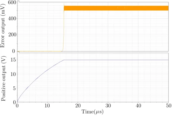
3.11 Regulation of positive output to 15 V . . . 48
3.12 Regulation of negative output to -15 V . . . 49
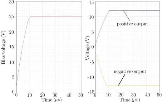
3.13 Simulation results when the bias is regulated to 25 V . . . 50
3.14 Simulation results when the bias is regulated to 30 V . . . 50
3.15 Simulation results when the bias is regulated to 45 V . . . 51
3.16 Simulation results of maximum load current and output power for different bias voltages . . . 51
3.17 Plots of maximum load current and output power for different bias voltages . . . 52
3.18 Oscilloscope trace when the bias voltage is regulated to 30 V. . 53
3.19 Voltage ripples on the positive and negative output. . . 53
3.20 Schematic of new bias circuit . . . 55
3.21 Positive charge pump and regulation circuits . . . 56
3.22 Negative charge pump and regulation circuits . . . 56
3.23 Layout of the designed circuit . . . 58
3.24 (a) Schematic of the op-amp; (b) Layout of the op-amp. . . 59
3.25 (a) Schematic of the gate regulator; (b) Layout of the pass-gate regulator. . . 60
3.26 Simulation results of maximum load current and output power for different bias voltages . . . 61
3.27 Positive and negative output when the bias voltage is regulated
to 30 V . . . 61
3.28 Bias voltages ripple and estimated chip size for different load capacitors . . . 62
4.1 Passive quenching circuit . . . 71
4.2 Typical structure of an active quench and reset circuit . . . 73
4.3 Diagram of AQRC in [21] . . . 74
4.4 Schematic of a monostable . . . 75
4.5 Modified monostable proposed in [23] . . . 75
4.6 Schematic of AQRC reported in [29] and [30]. . . 76
4.7 Diagram of AQRC in [33] . . . 77
4.8 Diagram of delay line technique in [33] . . . 78
4.9 Block diagram of high-resolution hold-off time control circuit . . 80
4.10 6-bit synchronous binary counter . . . 81
4.11 Layout of the proposed circuit . . . 82
4.12 Simulation model of the GM-APD . . . 83
4.13 Example of the circuit operation when the external inputs are set to 30 (“011110”) . . . 84
4.14 Hold-off times versus external input codes when the step reso-lution is set to 2 ns . . . 84
4.15 Setting range of the hold-off time for different step resolutions . 85 4.16 Block diagram of the new approach . . . 86
4.17 Photograph of the fabricated chip . . . 88
4.18 Top-side of the test PCB (holds the fabricated chip) . . . 89
4.19 Bottom-side of the test PCB (holds the tested APDs) . . . 89
4.21 a) Quenching pulse (Qp) and APD’s cathode voltage (Vcathode) with a hold-off time of 190 ns (00011101), (b)Vcathode with hold-off time = 326 ns (00110010) and (c)Vcathode with hold-off time
= 1.18µs (10110101). . . 91
4.22 External input codes versus hold-off time . . . 92
4.23 Plot of Vcathode for saturated count-rate . . . 92
5.1 Temperature control system in [15, 16]. . . 104
5.2 Gain stabilisation system in [8, 17]. . . 105
5.3 APD bias arrangement using two matched devices. . . 106
5.4 APD gain control and stablilization circuits in [22]. . . 107
5.5 Block diagram of proposed circuit. . . 108
5.6 Charge pump DC-DC converter. . . 109
5.7 Schematic of gain control circuit with two matched APDs. . . . 109
5.8 APD model and its simulation result. . . 111
5.9 Gain and the bias voltage of APD2 when its gain is set to 100. . 111
5.10 Photograph of the fabricated bias and gain control circuit gain. 112 5.11 Output voltages of charge pump DC-DC converter for different load currents. . . 113
5.12 Packaged two matched avalanche photodiodes. . . 113
5.13 Block diagram of the experimental setup. . . 114
5.14 Gain variation over a period of time under the control of the proposed circuit: (a) Gain set to 20; (b) Gain set to 50; (c) Gain set to 100. . . 115
5.15 APD’s performance when ambient temperature is changed. . . . 116
List of Tables
2.1 Characteristics of various semiconductors [1]. . . 13 4.1 Available hold-off times with AQRC in [33] . . . 79 4.2 Comparison of existing active quench and reset circuits . . . 95
Chapter 1
Introduction
1.1
Introduction
Advances in avalanche photodiode (APD) technology including higher sensitiv-ity, faster response time, lower operation voltage and lower costs have allowed APDs to replace PIN photodiodes or photomultiplier tubes (PMTs) in many low-light sensing applications.
In fibre communication systems, APDs have been the frequently choices as they can provide higher sensitivity in optical receivers than PIN photodiodes. Thanks to the high internal gain and fast response time, APD can achieve 5∼10 dB better sensitivity than PINs and provide higher signal to noise ra-tio (SNR) that make it more suitable for long haul communicara-tions as a high speed receiver in high bandwidth applications [1-3]. In single-photon counting and time-correlated single-photon counting (TCSPC) applications, APDs have been alternatives to photomultiplier tubes (PMTs). APDs can provide higher detection efficiency meanwhile give an excellent photon timing performance. More importantly, the APDs fabricated in planar technology compatible with CMOS circuits have enabled smaller size, lower operating voltage and lower power dissipation than the use of PMTs [4-6]. APDs are also well suited in some other applications including astronomy [7], fluorescence correlation spectroscopy [8], DNA sequencing [9, 10], quantum cryptography [11], LIDAR
[12-14], laser range finders [15, 16], metrology [17], confocal microscopy [18], particle detection [19] and nuclear medicine [20, 21].
Avalanche photodiodes operate in different modes under different bias voltages. The APD operates in linear mode with the bias voltage below its breakdown voltage. In this mode, APDs have their performance characterized by gain, noise, and bandwidth. The APD operates in Geiger-mode or single photon mode with the bias voltage above its breakdown voltage and in this mode have their performance characterized by dark count, hold-off time, afterpuls-ing, response time, jitter and responsivity. Performance characteristics such as quantum efficiency and spectral response are common to both modes of op-eration. To operate an APD in low light sensing applications, control circuits are required to bias it and also to optimize the APD to achieve the desired performance characteristics.
A number of control circuits have been designed by research groups to oper-ate the APDs and improve their performance. S. Cova et al have developed a number of quenching circuits for optimising the performance of GM-APDs. Those works were described in [22-24]. J. Kataoka et al. have developed a radiation detector consisting of APDs, an active gain control system and read-out circuitry that has been used in a satellite to monitor the distribution of low energy particles [25, 26]. D. Cronin and D. P. O’Connell have also de-veloped some control circuits for the APDs dede-veloped by the Photodetection and Imaging Group at University College Cork [27]. These circuits allow the user control of the APD characteristics such as gain and hold-off time [28, 29]. In some commercial organizations, APD control circuits have also been devel-oped. At Hamamatsu, circuits consisting of photodiodes and custom signal processing circuits have been developed which can be used for X-ray detection [30]. PerkinElmer have developed APD/preamplifier hybrid modules which
are used for confocal microscopy, range finding and LIDAR applications [31]. Some other organizations such as PicoQuant [32], ID Quantique [33] and Sensl [34] have also developed a number of systems that consist of APDs and control electronics for low light detection.
In this work, the design and development of three APD control circuits is described. These circuits were developed independently of each other. How-ever the combination of the three circuits results in a system that is capable of providing a more compact APD-based solution for a wide range of applications.
The first circuit designed is a bias circuit for an APD that can operate in both linear mode and Geiger-mode. The circuit was designed using AMS 0.35 µm and L-Foundry 0.15 µm CMOS process and post-layout simulations are pre-sented. Simulation results show that the circuit is capable of sourcing milliamp range load currents for shallow-junction planar APDs that operate up to 40 V. The layout of the circuit designed with the L-Foundry 0.15 µm process shows a small footprint of 1.55 mm × 1 mm, making it suitable for hybrid integra-tion with two external capacitors and an APD in a single package to operate seamlessly from a 5 V supply. This removes the requirement for a separate APD bias supply, employing the same supply for both signal conditioning and bias. Moreover, the circuit is capable of full integration for APD-based de-vices. Compared with the existing solutions including external high-voltage supplies, DC-DC converter chips and other reported designs (requiring several external components to function correctly), this design provides a more com-pact solution that can be used to reduce size, weight and power consumption for APD-based applications.
The second circuit designed is an active quench and reset circuit (AQRC) for the APD that operates in Geiger-mode. This circuit is designed with the aim of
overcoming the difficulties of hold-off time adjustment that remain in existing quench circuits. The circuit is simulated and layout designed in the Cadence design environment with L-Foundry 0.15 µm and AMS 0.35 µm CMOS pro-cess. The integrated circuit was fabricated using AMS 0.35µm CMOS process and tested with a GM-APD. Results show that this design is capable of linear changes to the hold-off time from several nanoseconds to microseconds with a reasonable step of 6.5 ns that allows setting of the optimal ‘afterpulse-free’ hold-off time for any GM-APD through digital inputs or additional signal pro-cessing circuitry. A minimum dead time of 28.4 ns was observed from the measurement, demonstrating a saturated photon-counting of 35.2 Mcounts/s with this AQRC.
The third circuit designed is a gain control circuit for APDs that operate in linear-mode. This circuit uses a matched APDs arrangement which has the advantages of controlling and stabilizing the gain without the need for exter-nal temperature sensing and control electronics thereby lowering the system cost and complexity. Meanwhile this design provides a simpler and more com-pact solution. The circuit was simulated in the Cadence environment with L-Foundry 0.15µm high voltage CMOS process, fabricated with discrete com-ponents (PCB) and measured with packaged APDs. Results show that the circuit can provide in excess of 40 V bias voltage for the planar APD and allow for the setting and stabilization of its gain independent of variation in the ambient temperature or power supply fluctuation.
1.2
Thesis Outline
This thesis is divided into a number of chapters. Chapter 2 introduces the theory of photodetection and the operation of avalanche photodiodes biased in linear mode and Geiger-mode. Chapter 3 describes a bias solution that is
used for APDs operating in both linear and Geiger modes. Chapter 4 presents the design and development of a new active quench and reset circuit (AQRC) for Geiger-mode avalanche photodiodes (GM-APDs). Chapter 5 describes a novel gain control and stabilization circuit for avalanche photodiodes (APDs) biased in linear mode. In Chapter 6, the conclusions of this thesis are made and future work is proposed.
Bibliography
[1] Joe C. Campbell, “Recent Advances in Telecommunications Avalanche Photodiodes”, IEEE Journal of Lightwave Technology, Vol.25, No.1, pp.109-121, 2007.
[2] Solomon Assefa, Fengnian Xia and Yurii A. Vlasov, “Reinventing germa-nium avalanche photodetector for nanophotonic on-chip optical intercon-nects”, Nature, Vol.464, No.7258, pp.80-84, Mar. 2010.
[3] Osayd Kharraz and David Forsyth, “Performance comparisons between PIN and APD photodetectors for use in optical communication systems”, International Journal for Light and Electron Optics, Vol.124, No.13, pp.1493-1498, Jul. 2013.
[4] A. M. Wallace, G. S. Buller, and A. C. Walker, “3D imaging and ranging by time-correlated single photon counting”, IEEE Journal of Computing and Control Engineering, Vol.12, No.4, pp.157-168, Aug. 2001.
[5] Massimo Ghioni, Angelo Gulinatti, Ivan Rech, Franco Zappa and Sergio Cova, “Progress in Silicon Single-Photon Avalanche Diodes”, IEEE Jour-nal of Selected Topics in Quantum Electronics, Vol.13, No.4, pp.852-862, Jul./Aug. 2007.
[6] F. Villa, B. Markovic, S. Bellisai, D. Bronzi, A. Tosi, F. Zappa, S. Tisa, D. Durini, S. Weyers, U. Paschen and W. Brockherde, “SPAD Smart
Pixel for Time-of-Flight and Time-Correlated Single-Photon Counting Measurements”, IEEE Photonics Journal, Vol.4, No.3, pp.795-804, Jun. 2012.
[7] M. Martinez, A. Ostankov, E. Lorenz, R. Mirzoyan, and T. Schweizer, “Contraints in using APDs in air Cherenkov telescopes for y-astronomy”, Nuclear Instruments and Methods in Physics Research A, Vol.442, No.1-3, pp.209-215, Mar. 2000.
[8] M. Oda, Y. Yamashita, E. Ohmae, and Y. Tsuchiya, “Tissue oxygenation monitoring with a time-resolved spectroscopy system”, CLEO Pacific Rim Conference on Lasers and Electro-Optics, pp.378-379, Jul. 2001.
[9] S. Fore, T. A. Laurence, Y. Yeh, R. Balhorn, C. W. Hollars, M. Cos-man, and T. Huser, “Distribution analysis of the photon correlation spec-troscopy of discrete numbers of dye molecules conjugated of DNA”, IEEE Journal of Selected Topics in Quantum Electronics, Vol.11, No.4, pp.873-880, Jul. 2005.
[10] S. A. Soper, J. H. Flanagan, B. L. Legendre, D. C. Williams, and R. P. Hammer, “Near-infrared, laser-induced fluorescence detection for DNA sequencing applications”, IEEE Journal of Selected Topics in Quantum Electronics, Vol.2, No.4 pp.1129-1139, Dec. 1996.
[11] G. Ribordy, N. Gisin, O. Guinnard, and H. Zbinden, “Single-photon detec-tion at telecom wavelength and quantum cryptography”, Annual Meeting of the IEEE Lasers and Electro-Optics Society, pp.771-772, 2003.
[12] B. Dion, P. Iepage, C. Iedoux, and N. Bertone, “High performing pho-todiodes for demanding applications”, LEOS Summer Topical Mettings, pp.48-49, Jul. 2006.
[13] T. Maruyama, F. Narusawa, M. Kudo, M. Tanaka, Y. Saito, T. Yoshida, and A. Nomura, “A near-infrared photon-counting system using an In-GaAs avalanche photodiode”, Conference on Lasers and Electro-Optics, pp.138-139, May 2000.
[14] Y. Kawamura and T. Imai, “Development of spaceborne LIDAR: ELISE (Experi-mental Lidar In Space Equipment)”, CLEO/Pacific Rim Confer-ence on Lasers and Electro-Optics, pp.270271, Aug. 1999.
[15] J. S. Massa, M. Umasuthan, A. M. Wallace, G. S. Buller and A. C. Walker, “Rangefinding using time correlated single photon counting”, IEEE Inter-national Conference on Recent Advances in 3-D Imaging and Modeling, pp.36-43, May 1997.
[16] Emmanuel R. Moutaye and Hlne Tap-Bteille, “CMOS Avalanche Photo-diode Embedded in a Phase-Shift Laser Rangefinder”, IEEE Transactions on Electron Devices, Vol.55, No.12, Dec. 2008.
[17] T. Miyata, T. Araki, and T. Iwata, “Correction of the intensity-dependent phase delay in a silicon Avalanche Photodiode by controlling its re-verse bias voltage”, IEEE Journal of Quantum Electronics, Vol.39, No.7, pp.919-923, Jul. 2003.
[18] Y. Zhang and A. Roorda, “Photon signal detection and evaluation in the adaptive optics scanning laser ophthalmoscope”, Journal of the Optical Society of America, Vol.24, No.5, pp.1276-1283, May 2007.
[19] S. M. Khanna, S. Charbonneau, P. G. Piva, M. Parenteau, and C. Carlone, “Effects of 3 MeV proton irradiation on the excitonic lifetime in gallium arsenide”, IEEE Transactions on Nuclear Science, Vol.45, No.1, pp.2430-2435, Dec. 1998.
[20] J.-F. Pratte, S. Robert, G. De Geronimo, P. O’Connor, S. Stoll, C. M. Pepin, R. Fontaine, and R. Lecomte, “Design and performance of 0.18um CMOS charge preamplifiers for APD-based PET scanners”, IEEE Trans-actions on Nuclear Science, Vol.51, No.5, pp.1979-1985, Oct. 2004. [21] M. C. Maas, D. J. van der Laan, D. R. Schaart, J. Huizenga, J. C.
Brouwer, P. Bruyndonchx, S. Leonard, C. Lemaitre, and C. W. E. van Eijk, “Experimental characterization of monolithic-crystal small animal PET detectors read out by APD arrays”, IEEE Transactions on Nuclear Science, Vol.53, No.3, pp.1071-1077, Jun. 2006.
[22] S. Cova, M. Ghioni, A. Lacaita, C. Samori and F. Zappa, “Avalanche photodiodes and quenching circuits for single-photon detection”, Applied optics, Vol.35, pp.1956-1976, 1996.
[23] F. Zappa, M. Ghioni, S. Cova, C. Samori and A. Giudice, “An integrated active-quenching circuit for single-photon avalanche diodes”, IEEE Trans-actions on Instrumentation and Measurement, Vol.49, pp.1167-1175, 2000. [24] F. Zappa, A. Lotito, A. Giudice, S. Cova and M. Ghioni, “Monolithic active-quenching and active-reset circuit for single-photon avalanche de-tectors”,IEEE Journal of Solid-State Circuits, Vol.38, pp.1298-1301, 2003. [25] J. Kataokaa, R. Satoa, T. Ikagawaa, J. Kotokua, Y. Kuramotoa, Y. Tsubukua, T. Saitoa, Y. Yatsua, N. Kawaia, Y. Ishikawab and N. Kawa-batab, “An active gain-control system for Avalanche photodiodes under moderate temperature variations”, Nuclear Instruments and Methods in Physics Research A, Vol.564, No.1, pp.300-307, 2006.
[26] J. Kataoka, T. Toizumi, T. Nakamori, Y. Yatsu, Y. Tsubuku, Y. Ku-ramoto, T. Enomoto, R. Usui, N. Kawai, H. Ashida, K. Omagari, K. Fujihashi, S. Inagawa, Y. Miura, Y. Konda, N. Miyashita, S. Matsunaga,
Y. Ishikawa, Y. Matsunaga and N. Kawabata, “In-orbit performance of avalanche photodiode as radiation detector on board the picosatellite Cute-1.7+APD”, Journal of Geophysical Research, Vol.115, A05204, May 2010.
[27] http://www.ucc.ie/en/eleceng/research/researchareas/photodectect/ [28] Diarmuid Patrick O’Connell, “Control circuit for Avalanche
Photodi-odes”, Ph.D. thesis, University College Cork, Cork, Ireland, Feb. 2009. [29] Donal Cronin, “Automatic Control Circuits for Geiger-Mode Avalanche
Photodiodes”, Ph.D. thesis, University College Cork, Ireland, Mar. 2009. [30] https://www.hamamatsu.com/jp/en/product/category/3100/4005/ 4122/index.html. [31] http://www.perkinelmer.co.uk/PDFS/downloads/ cat sensorsandemittersphotondetection.pdf [32] http://www.picoquant.com/ [33] http://www.idquantique.com/ [34] http://sensl.com/
Chapter 2
Introduction to avalanche
photodiodes (APDs)
This chapter briefly introduces the theory of photodetection and the operation of avalanche photodiodes (APDs). The APD’s physical processes and key performance characteristics are explained. The backgrounds of some external control circuits required for the APDs’ operation are described. The design of the planar APD used throughout this project is illustrated.
2.1
Photodetection
Based on photon absorption in semiconductor materials, a photodetector ab-sorbs light via three processes including intrinsic band-to-band absorption, free carrier absorption and band-to-impurity absorption, see Figure 2.1. In-trinsic band-to-band absorption occurs when the photon energy (hν) is greater than the material bandgap energy Eg. In this case, a photon is able to ex-cite an electron from the valence band up into the conduction band to create an electron-hole pair. The hole and electron each constitute a charge carrier. The electric field applied to the semiconductor will cause the hole and electron to be transported into the external circuit through the material. When the electron-hole pair makes its way to the external circuit their combined effect will lead to a flow of charge q in the circuit where q is the charge of a single
electron [1], [2].
Appllied electric field Conduction band Electron Valance band Hole Intrinsic Band-to-Band Absorption Free Carrier
Absorption Band-to-ImpurityAbsorption
Acceptor level Donor level
hv
hv
hv
hv
Figure 2.1: Photon absorption mechanisms.
Intrinsic band-to-band absorption is the dominant absorption mechanism in most semiconductors used for photodetection. To create an electron-hole pair, it requires that the photon energy, E =hν, is greater than the material bandgap energy, Eg: this can be expressed as
hv > Eg or h
c
λ > Eg (2.1)
This yields a maximum allowable wavelength
λmax = hc Eg or λmax(nm) = 1240 Eg(eV) (2.2) Where Eg (eV) = bandgap energy in electron-volts.
Table 2.1 lists the bandgap, the corresponding maximum usable wavelength, and typical operating wavelengths for common semiconductor materials. Free carrier absorption occurs when the photon energy is absorbed by free carriers in either the conduction band or the valence band which corresponds to the “heating” of the semiconductor material. It is a secondary effect at the near infrared wavelengths used for optical communications. Band-to-impurity
Material Bandgap Maximum wave-length (nm) Typical operat-ing range (nm) Si 1.12 1110 500 - 900 Ge 0.67 1850 900 - 1300 GaAs 1.43 870 750 - 850 InxGa1−xAsyP1−y 0.38 - 2.25 550 - 3260 1000 - 1600 Table 2.1: Characteristics of various semiconductors [1].
absorption is another secondary effect at near-IR wavelengths. It is used to construct photodetectors responsive at mid-IR wavelengths as long as 30 µm [1].
An important parameter for a photodiode is the quantum efficiency (QE). The quantum efficiency is defined as the probability that a single photon incident on the detector generates an electron-hole pair and is given by [1]:
η = number of e −h pairs produced
number of incident photons (2.3)
where 0≤η≤1. A signal with photon energy sufficient to generate photocarriers will continuously lose energy to the semiconductor crystal lattice as the optical field propagates through the semiconductor. As can be seen from Figure 2.2, there is a reflection loss at the interface of the air and the semiconductor due to differences in the index of refraction. The Fresnel reflectivity for an optical signal at normal incidence to an interface between two materials is given by
R = (n1−n2)
2
(n1+n2)2
(2.4) where n1 = index of refraction of first material and n2 = index of refraction
of second material. For many semiconductors used in the 800 nm to 1500 nm region, n is between 3.2 and 3.6 and the reflectivity can be as high as 32 %. Reflection losses can be reduced with antireflection coatings to less than 1 %.
Inside the semiconductor, the field decays away exponentially as energy is transferred to the semiconductor. The material can be characterised by an
hv Power Pi Pi(1−R) Pi(1−R)e−αx 0 Position Semiconductor Penetration depth 1/ Pi = incident power R = reflectivity of semiconductor = absorption length α α
x
Figure 2.2: Optical absorption in a semiconductor [1].
absorption constant α and a penetration depth 1/α. Penetration depth is the point at which 1/e of the optical signal power remains. The power in the optical field decays with distance. The amount of power absorbed in the semiconductor is as a function of position within the material and can be expressed as
Pabs =Pi(1−R) 1−e−αx
(2.5) The number of photons absorbed per second is the power in watts divided by the photon energy (E = hν). If each absorbed photon generates a pair of photocarriers (i.e. an electron-hole pair), the number of photocarriers gener-ated per photon for a specific semiconductor with reflectivity R and absorption constant α is given by
η(x) = (1−R) 1−e−αx
(2.6) Where η(x) is the quantum efficiency of the photodetector.
Responsivity is defined as the ratio of the photocurrent to the optical power and is given by [2] R= Iphoto Popt = ηq hv(A/W) (2.7)
Where Iphoto = photogenerated current, Popt = incident optical power, η = quantum efficiency, q = electronic charge, h = Planck’s constant, v = optical frequency. For an ideal photodiode each incident photon would generate the charge of one electron flowing in the external circuit. In reality, there are sev-eral physical effects that tend to reduce the responsivity, including incomplete absorption, recombination, reflection from the semiconductor surface and con-tact shadowing.
The responsivity of a semiconductor will also vary with wavelength [1]. Re-sponsivity increases as the wavelength increases because there are more pho-tons per watt at long wavelengths than there are at short wavelengths. This is a direct result of the photon energy decreasing with wavelength. Since the amount of photocurrent is determined by the number of photons instead of the energy of the photons, longer wavelengths generate more photocurrent per watt than the short wavelengths.
2.2
Avalanche photodiodes
An avalanche photodiode (APD) is a very sensitive photodetector. The ad-vances in APDs such as low operating voltages, low-cost, higher sensitivity and small-size make it very attractive for use in photodetection [1]. It has been used in a wide range of lowlight sensing applications including astronomy [3], DNA sequencing [4], light detection and ranging (LIDAR) [5] and medical sensing [6].
2.2.1
Avalanche effect in APDs
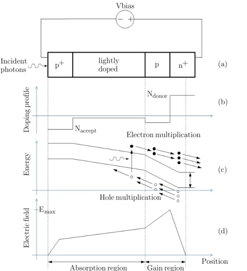
In Figure 2.3, the structure of a typical avalanche photodiode is illustrated [1]. The APD consists of four sections of semiconductor with different doping profiles as shown in Figure 2.3(b). The leftmost section is a p-type semicon-ductor doped to a density of Naccept, while the rightmost section is an n-type semiconductor doped to a density Ndonor. The middle region is an intrinsic region in combination with a second p-type region. The energy diagram of the APD is shown in Figure 2.3(c) while the electric field profile of the space charge region is shown in Figure 2.3(d). When a p-n junction is subjected to a high reverse bias there are two breakdown mechanisms that can occur. The first mechanism involves the atoms being directly ionized by the applied field which is known as zener breakdown and is commonly used to make volt-age regulating diodes. The second mechanism is called avalanche breakdown which is caused by high velocity carriers causing impact ionisations within the semiconductor that generates additional carriers.
In the absorption region shown in Figure 2.3(d), photons are absorbed in the lightly doped semiconductor material, generating electron-hole pairs. The carriers rapidly travel through the lower field drift region at their saturation velocity (1×107 cm/s for electric field > 104 V/cm [7]) to the edges of the
region. Carriers that reach the gain region are further accelerated by an even higher electric field. Avalanche breakdown then begins to occur with very high velocity carriers causing impact ionisations within the semiconductor that will further generate additional carriers. These additional carriers can then undergo additional impact ionisations causing an avalanche effect.
Vbias p+ p n+ Ndonor Naccept Incident photons Electron multiplication Hole multiplication Emax Position Absorption region Gain region
Doping profile Energy Electric field (a) (b) (c) (d) lightly doped
Figure 2.3: Example of an avalanche photodiode. (a) Diode structure. (b) Doping profile. (c) Energy band diagram. (d) Electric field profile. [1]
2.2.2
Impact ionisation
The impact ionisation or multiplication process in the gain region is demon-strated in Figure 2.4. The avalanche current flowing in the APD is caused by this mechanism. The impact ionisation can be characterised by the ionisation coefficients, αe and αh, for electrons and holes respectively. αe and αh can also be defined as the number of secondary electron-hole pairs generated in a unit distance with the applied electric field. For a given temperature, the ionization coefficients are exponentially dependent on the electric field and can
be defined as αe,h =a.exp − b E c cm−1 (2.8) where a, b and c are experimentally determined constants, E = magnitude of the electric field.
Electric field
distance Single electron
enter gain region
Single electron enter gain region
Holes move to negative end Holes move to negative end time time distance Electric field Electron causes impact ionization Electron causes impact ionization Hole causes impact ionization (a) (b)
Figure 2.4: (a) Impact ionisation process with electrons only contributing (b) Impact ionisation process with both holes and electrons contributing; note the avalanche direction indicated by the blue arrow [1].
the number of non-ionising collisions with thermally excited atoms and the phonon energy as shown in Eqn. 2.9. The additional phonon collisions reduce the carrier velocity and decreases their probability of gaining sufficient energy to initiate impact ionisations and the generation of the number of secondary electron-hole pairs will be decreased [8-13].
αe,h= qε Ei exp −3EphononEi (qελ)2 (2.9) where q = electronic charge, E = electric field,Ephonon = phonon energy,Ei = ionisation threshold energy (minimum energy for impact ionisation to occur),
λ = mean free path for phonon scattering.
To determine the ionising carrier in an APD, an ionisation ratio is defined as:
k= αh
αe
(2.10) The APD structure is optimised for the more ionising carrier depending on this ratio k. For materials where αe αh, (i.e. where electrons are much more ionising than holes such as in silicon) it is required that photons are absorbed in the p-region (see Figure 2.3). Values of k between 0.01 and 0.003 can be achieved to produce high quality Si APDs. Similarly, for materials where holes are more ionising than electrons (αh αe, e.g. Germanium), photons should be absorbed at the n-region of the junction. Figure 2.4(a) shows the impact ionisation process for silicon (k 1), where holes do not contribute. When a photoelectron enters into the gain region, it is accelerated by the applied electric field and then gains enough kinetic energy from the field to generate a series of impact ionisations. In this example, it results in six extra electrons and the avalanche proceeds in a well defined manner from left to right. It is assumed that only holes contribute to the impact ionisations when k 1. Figure 2.4(b) demonstrates an undesirable case where k∼= 1 and both electrons and holes contribute to the impact ionisations. In this example,
an electron initiates the first ionisation but the subsequent ionisations can be caused by high energy electrons or holes. This avalanche process behaves in an uncontrolled manner, moving back and forth in the gain region depending on which carrier is causing the ionisation. This leads to an undesirable uncertainty associated with this type of process as there is no clearly defined end point until all possible impact ionisations are completed [1, 2]. The net result of this is an undesirable noise contribution due to the stochastic nature of impact ionisation called excess noise.
2.2.3
Multiplication gain
The gain or multiplication factor of an APD is given by [2, 7]
M = Iphoto
Iprimary
(2.11) Where Iphoto = observable photocurrent at APD terminals, Iprimary = internal photocurrent before multiplication. The primary current is defined by
Iprimary =
ηq
hvPrcvd (2.12)
Whereη= quantum efficiency,Prcvd= received optical signal power. Typically, multiplication gains of a few tens to a few hundreds are applied, even though it is possible for the multiplication factor to be as high as 103 or 104 [1, 14].
The expressions for electron multiplication (Me) and hole multiplication (Mh) in a gain region of lengthlg are [1, 2, 7]
Me = 1 1−Rlg l0 αeexp − Rx 0 (αe−αh)dx dx (2.13) Mh = exp−Rlg 0 (αe−αh)dx 1−Rlg l0 αeexp − Rx 0 (αe−αh)dx dx (2.14)
As both αe and αh in most devices are functions of position within the gain region, exact solutions to Equations 2.13 and 2.14 are difficult to obtain. In certain cases closed form solutions are available. One is for the case whereαe = αh, only electrons are being injected into the gain region, the electric field in the gain region is uniform and the number of ionising collisions per primary carrier is large. In this case, the electron multiplication is given by
Me =
1−k
exp(−(1−k)αelg)−k
(2.15) Where lg = length of gain region. For the case where k = 0, Equation 2.15 can be reduced to
Me= 1 1−αelg
(2.16) Instability occurs for lg = 1/αe and this condition must be avoided. In a practical device, the maximum achievable DC multiplication is limited by the series resistance and space charge effect (these factors can be combined into a single series resistance R). The multiplication for photogenerated carriers can be described as [2, 15] Me = I−IM D IP −ID = h 1 1−VR−IR VB ni (2.17)
Where I = total multiplied current,IP = total primary (unmultiplied) current,
ID = primary dark current, IM D = multiplied dark current, VR = reverse bias voltage, VB = zener breakdown voltage, n = constant depending on the semiconductor material, doping profile and radiation wavelength. For high light intensity,IP IDandIRVB, the maximum value of the multiplication is given by kk(Mph)max ∼= I IP = h 1 1−VR−IR VB ni |VR→VB≈ 1 nIR/VB (2.18)
or
(Mph)max =
p
VB/nIPR (2.19)
When the photocurrent is smaller than the dark current, the maximum multi-plication is limited by the dark current and is given by an expression similar to Equation 2.19, with IP replaced by ID. It is important that the dark current is made as low as possible so that it does not limit (Mph)max.
2.3
APD operation modes
With different bias voltages, avalanche photodiodes operate in different modes. APDs that are biased below the breakdown voltage (linear mode) have their performance characterized by gain, excess noise, responsivity and bandwidth while APDs biased above the breakdown voltage (Geiger-mode) have their performance characterized by photon detection probability, dark count rate, hold-off time, afterpulsing effect, and response time jitter. Some performance characteristics such as quantum efficiency and spectral response are common to both modes of operation.
2.3.1
Linear mode
Linear mode applies to APDs biased below the breakdown voltage. In linear mode, the current output varies linearly with the incident optical power and the gain to the incident photo-generated carriers can be from one up to several hundred.
The bandwidth associated with avalanche photodiodes is limited by three main factors including RC time constant, transit time and avalanche multiplication build-up time. The RC time constant is determined by the parallel plate capacitor which shunts current away from the external circuit and the junction
resistance. The junction capacitance is determined by the APD geometry, the fabrication process and applied bias. Since the duration of the photocurrent depends on the lifetime of the longest lived carrier, any fluctuations in the received optical field faster than the carrier lifetime will not be clearly observed. An overall estimate for the APD bandwidth is given by the root-sum-square of the two individual bandwidths [16].
B = r 1 1 fRC 2 +1 ft 2 (2.20)
Where fRC = RC bandwidth, ft = transit time bandwidth. The time delay due to avalanche multiplication build up can also affect APD bandwidth. The bandwidth of an avalanche photodiode has been shown to be independent of avalanche multiplication when the DC multiplication is less than αe/αh [17]. In this circumstance the bandwidth is given by Equation 2.20. Other factors that affect response speed are carrier diffusion current from outside the gain region and the space charge effect. The time delay of carriers generated out-side the gain region occurs when the absorption region is not wide enough with respect to the penetration depth of the incident light. The space charge effect is evident when the incident light level is high and the resulting photocurrent is large, with the attractive power of the electron-hole pairs diminishing the electric field effect.
Similar to a passive component, the APD generates signal noise that can be characterised into a number of types. Thermal noise is a temperature depen-dent white noise source. The thermal noise generated by an APD is given by
¯
v2
R= 4kT RLB (2.21)
load resistance, B = the bandwidth. The load resistance is the series resistance connected to the APD as well as the APD resistance itself.
Shot noise is a current dependent white noise source. The total shot noise generated by an APD is given by Equation 2.22:
¯
i2 = 2qIB (2.22)
Where q = electron charge, I = total APD current, B = the bandwidth. The total current is made up of the dark current and the photocurrent. The dark current has a surface leakage component, IDS, that does not flow through the gain region and so does not take part in the multiplication process. On the other hand the internal dark current component, IDG, flow through the gain region and adds to the gain current.
The ionization of individual carriers is not uniform and so the multiplication process contains statistical fluctuations known as excess noise. The excess noise factor, F, can be expressed by the multiplication ratio, M and the ratio of the electron/hole ionization rate, k, and is defined as [16, 18]:
F =M k+ 2− 1 M (1−k) (2.23)
Equation 2.23 is the noise factor when electrons are injected into the avalanche region. To evaluate the excess noise factor when holes are injected into the avalanche region, k in Equation 2.23 should be substituted by 1/k. In the ideal case noise is minimized, k should equal zero for electron injection and k should be infinite for hole injection. Silicon APDs are usually used when electrons are injected into the avalanche region. When the thermal effects and total current noise are taken into account the final expression for APD noise is given as:
¯ I2 D = 2q(IP +IDG)M2F B+ 2qIDSB+ 4kT B RL (2.24)
Where IP is the photocurrent for M=1. From Equation 2.24 it can be seen that excess noise increases as the gain increases. The photocurrent generated by the optical signal is also amplified by the gain and as a result there is an optimum gain value which maximizes APD signal to noise performance. This optimum gain is achieved when the shot noise equals the thermal noise, as shown in Figure 2.5 [16, 19]. Gain Noise Signa l = (IPM )Rin
Thermal Noise = 4FampkTBRin
S/N Max. Mopt Shot Noise = in 2 PM FBR qI 2
FAMP: Noise figre of next stage amplifier
Rin: Input resistance of next stage amplifier
: Noise figure of next stage amplifier
FAMP
Figure 2.5: Signal and Noise versus gain [19]. The signal to noise ratio for an APD can be calculated as follows:
S/N = I 2 PM2 2q(IP +IDG)BM2F + 2qIDS +4kT BR L (2.25) Operating conditions such as temperature and bias voltage play a large part in determining the APDs performance. The APD gain has a temperature dependent characteristic [16, 20]. The gain at a certain bias voltage decreases with increasing temperature. These effects can be seen in Figure 2.6.
0 10 20 -20 -10 10 20 30 50 70 100 390V 380V 370V 350V 330V 310V 1 2 5 10 20 50 100 0 100 200 300 400
Bias voltage (V) Temperature (deg C)
From -20 to +20 deg (left to right)
Figure 2.6: Gain variations of APD as a function of bias voltage and temper-ature [20].
the APD gain close to the optimum gain and stabilize it. This is accomplished by maintaining a constant temperature or adjusting the bias voltage according to the changes in temperature using appropriate control circuits. Those cir-cuits will be introduced in more detail in Chapter 5 and a new bias and gain control circuit will be presented which can be used to maintain the APD gain independent of environmental conditions.
2.3.2
Geiger-mode
Geiger-mode avalanche photodiodes are capable of operating as single photon counting diodes or single photon avalanche diodes (SPAD). In Geiger-mode, the APD is biased above its breakdown voltage. When a photon is absorbed by the APD, an avalanche event is triggered and registered as a photon count. External circuitry, known as a quench circuit, senses this event and reduces the bias across the APD to allow it to recover. After the current dissipates, the voltage is reset, and the diode can count another avalanche event [21]. In contrast to the APD operating in linear mode, the output of a Geiger-mode
Incident optical power I(t) I(t) (a) (b) t t t
Figure 2.7: Photocurrent when APD operates in (a) linear mode and (b) Geiger-mode.
APD is not a linear current, but current pulses. The difference between oper-ating an APD in the linear-mode and the Geiger-mode can been seen in Figure 2.7, where the photocurrent of the former is proportional to the incident optical power while the light intensity on a Geiger-mode APD gives a corresponding change in the number of current pulses per second [12]. Operating the APD in Geiger-mode eliminates many of the current fluctuations present in the lin-ear mode. The output current pulses are sufficiently high so that variations between pulses do not matter. The external circuitry only detects that a pulse has occurred [21].
Dark count
When counting photons, the GM-APD detects the avalanche events created in the APD. The avalanche breakdowns are not only generated by photon absorp-tion but also by other means such as thermal generaabsorp-tion of electron-hole pairs and carriers tunnelling across the depletion region [7, 12, 21, 22, 23]. These pulses result in a noise source for the Geiger-mode detector and are referred to as dark counts due to the detection of events in the absence of a light source. The dark count rate of a GM-APD is an important parameter that should be minimised. Shockley-Reed-Hall (SRH) generation and recombination theory describes the thermal excitation of carriers in semiconductors. If an electron-hole pair is thermally generated in the depletion region, an avalanche event may occur as outlined in Section 2.2.1. If these are generated in the p-epilayer region of the GM-APD, these carriers may drift to the depletion region and cause an avalanche [12, 24]. Band-to-band tunnelling contributes to the num-ber of dark counts if the electric-field strength is high (5 ×10⁵ V cm−1) [24,
25]. However, high electric-fields are required in GM-APDs to maximise the photon detection probability [21]. Due to these high electric-fields, an elec-tron may tunnel from the valence band to the conduction band, thus leaving a hole behind in the valence band. As a result, the electron-hole pair may generate an avalanche event and hence a dark count. When the acceptor con-centration of the p-region of the GM-APD’s pn junction is increased, i.e. Na
≥ 5×1015 cm−3, and hence the breakdown voltage, V
br, is less then 25 V, the field strength in the junction is increased such that the dark count rate due to tunnelling is increased. When operating the GM-APD, the dark count rate will increase as the following parameters increase: excess bias voltage (the bias voltage above the breakdown voltage), detector area and temperature [21, 26-30]. Decreasing the excess bias will decrease the dark count but unfortu-nately the photon detection probability will also be reduced. Decreasing the
active area is possible but may not suit all applications such as imaging. The temperature dependence of the dark count can be minimised by cooling the GM-APD using a thermoelectric cooler (TEC) [12].
Afterpulsing
During an avalanche event, some of the charge carriers will be captured by trapping centres in the space charge region when the avalanche current flows through the device and there are released after a period of time. These carriers could trigger a new avalanche event, which in turn can lead to further carrier trapping. The avalanche events triggered by trapped carriers are not related to new photon arrivals and are thus an unwanted source of noise called after-pulsing. Afterpulsing intensity depends on the type and number of trapping centres present in the device and the amount of charge that flows through the junction during an avalanche. Afterpulsing introduces correlation between consecutive avalanches, and limits the maximum repetition rate and so needs to be minimised.
The afterpulsing phenomenon can be minimized by allowing sufficient time for all trapped charge to dissipate before resetting the GM-APD. This is achieved using an appropriate control circuit that quenches the APD avalanche current by lowering the bias voltage below the breakdown voltage, holding the bias below breakdown for a period of time before resetting the device to its original bias voltage to await the next avalanche event. The period of time that the device is held below its breakdown voltage is known as the hold-off time. During the hold-off and reset process, no incoming photon can be detected and this leads to a reduction of the maximum achievable count-rate of the GM-APD. As a result, a trade-off needs to be made between the count-rate and an acceptable level of afterpulsing. The control circuits used to minimize the afterpulsing phenomenon and setting the hold-off time will be discussed
in detail in Chapter 3 and a quenching circuit with improved hold-off time control logic for the GM-APD will be introduced.
Jitter
Timing jitter is the delay between a photon being absorbed by the detector and the detector sending out a measurable response. It can be described as the full-width half-maximum measure of the temporal variation in the avalanche break-down pulses resulting from an incident photon. Among the timing-resolution components are the variation caused by the generated carrier transit time from the depletion layer to the multiplication region, which is dependent on the depth of absorption of the incident photon and the statistical build up of the avalanche current itself [21, 26, 32].
2.4
Planar APD
The APD used throughout this research is the planar junction APD developed by the Photodetection and Imaging Group at University College Cork [33, 34]. A cross section of the APD can be seen in Figure 2.8. The APD can be fabricated with CMOS compatible process steps with the p-epitaxy common to the CMOS process that allows the APD to be monolithically integrated with CMOS circuitry. The central p-implant is the enrichment implant that increases the p-doping compared to the epi-layer. The overlap of the p and n layers defines the active area of the detector. The high field region is the depletion region that occurs around the pn junction where the photoelectron impact ionisation takes place. The n+ layer overlaps the high-field region into the p-epitaxial substrate, forming a virtual guard ring. The guard ring elim-inates edge breakdown of the diode caused by the junction curvature effects, allowing a uniform breakdown across the surface of the junction. The n+ layer forms the diode’s cathode. The annular p+ sinkers allows top contact to the
anode which aid in the removal of metallic contaminants from the high-field region [16, 35, 36]. The shallow junction of the planar APD gives the detector increased sensitivity to short wavelength light (400 to 650 nm). The doping of the junction is engineered to allow for low voltage operation (<50 volts).
hv
Cathode Anode
P- epitaxy P+ substrate
Figure 2.8: Cross section of planar shallow junction APD developed by the Photodetection and Imaging Group at University College Cork [2, 33, 34]. Planar APDs have a number of advantages over Large Area APD (LAAPD) bevelled edge structures and reach-through APD structures. In LAAPDs the impact ionisation takes place in the p-region where the electric field is low. It takes substantial time, 10ns-30ns, for multiplication and charge collection to take place. LAAPDs need a large operating voltage of between 1000 and 2000 volts. Cooling systems, such as liquid nitrogen, are needed for LAAPDs to operate in photon counting applications. Reach through APDs have high operating voltages of between 300 - 450 volts. Also, placing the high field region deep inside the detector structure and the use of a pi region requires specialised processing steps. These steps increase fabrication costs and are not CMOS compatible [2, 16]. The planar APD has a simple structure requiring fewer process steps. This leads to fewer defects and higher performance detectors. Moreover, the low operation voltage (< 50 V) makes it possible to design an on-chip bias circuit to power the APD. As will be seen in Chapter 3, an
intergrable bias solution is designed for biasing the planar APD that can be used to reduce the size, weight and power consumption of the APD-based applications.
2.5
Conclusion
This chapter has introduced the theory of photodetection and some back-ground detail of APDs that operate in both linear and Geiger modes. The performance characteristics of the APD such as quantum efficiency, multipli-cation gain, bandwidth, dark count and afterpulsing have been discussed. The APD requires many external control circuits for enhancing its performance. In the following chapters, some of these control circuits will be introduced and improved circuit designs will be presented. These circuits include a bias circuit, a gain stabilization circuit and a quenching circuit. The bias circuit is used to provide the high bias voltage for powering the APDs that operate in both linear and Geiger modes. The quenching circuit is used to perform photon counting while minimising the afterpulsing phenomenon in the Geiger-mode APDs. The gain stabilization circuit is designed for the APD that operates in linear mode to control and maintain its gain independent of temperature and power supply fluctuations.
Bibliography
[1] S.B. Alexander, Optical Communication Receiver Design, SPIE, 1997. [2] Aoife M. Moloney, “A CMOS Monolithically Integrated Photoreceiver
In-corporating an Avalanche Photodiode”, Ph.D. thesis, Department of Elec-trical and Electronic Engineering, University College Cork, April 2003. [3] D. Pellion, K. Jradi, A. Le Padellec, A. Rennane, F. Moutier, V. Borrel, D.
Esteve, C. Magenc and A. R. Bazer-Bachi, “Geiger avalanche photodiodes as tentative light detectors for VHE gamma ray astronomy”, Experimental Astronomy, Vol.27, No.3, pp.187-195, 2010.
[4] K. Healy, B. Schiedt, and A. P. Morrison, “Solid-state nanopore technolo-gies for nanopore-based DNA analysis”, Future Medicine, Vol.2, No.6, pp.875-897, Dec. 2007.
[5] A. Michael Krainak, X. Sun, G. Yang and W. Lu, “Comparison of linear-mode avalanche photodiode lidar receivers for use at one-micron wave-length”, Proc. SPIE 7681, 76810Y(2010)
[6] F. Powolny, E. Auffray, H. Hillemanns, P. Jarron, P. Lecoq, T. C. Meyer and D. Moraes, “A Novel Time-Based Readout Scheme for a Combined PET-CT Detector Using APDs”, IEEE Transactions on Nuclear Science, Vol.55, No.5, pp.2465-2474, Oct. 2008.
[7] S. M. Sze. Semiconductor Devices Physics and Technology. Wiley, 2nd edition, 2001. ISBN:0471333727.
[8] P. Bhattacharya. Semiconductor Optoelectronic Devices. Prentice Hall, 2nd edition, 1994. ISBN:0138057486.
[9] P. A. Wolff, “Theory of electron multiplication in silicon and germanium”, Physical Review, Vol.95, No.6, pp.1415-1420, Sep. 1954.
[10] R. J. McIntyre, “A new look at impact ionization-Part I: A theory of gain, noise, breakdown probability, and frequency response”, IEEE Transac-tions on Electron Devices, Vol.46, No.8, pp.1623-1631, Aug. 1999.
[11] P. Yuan, K. A. Anselm, C. Hu, H. Nie, C. Lenox, A. L. Holmes, B. G. Streetman, J. C. Campbell, and R. J. McIntyre, “A new look at impact ionization-Part II: Gain and noise in short avalanche photodiodes”, IEEE Transactions on Electron Devices, Vol.46, No.8, pp.1632-1639, Aug. 1999. [12] Donal Cronin, “Automatic Control Circuits for Geiger-Mode Avalanche Photodiodes”, Ph.D. thesis, University College Cork, Ireland, Mar. 2009. [13] C. L. Anderson and C. R. Crowell, “Threshold Energies for Electron-Hole Pair Production by Impact-Ionization in Semiconductors”, Physical Review B, Vol.5, No.6, pp.2267-2272, Mar. 1972.
[14] X. Sun and F.M. Davidson, “Photon Counting with Silicon Avalanche Photodiodes”, IEEE Journal of Lightwave Technol, Vol.10, No.8, pp.1023-1032, Aug. 2008.
[15] H. Melchior and W.T. Lynch, “Signal and Noise Response of High Speed Germanium Avalanche Photodiodes”, IEEE Transactions on Electron De-vice, Vol.13, No.12, pp.829-838, Dec. 1966.
[16] Diarmuid Patrick O’Connell, “Control Circuits for Avalanche Photodi-odes”, Ph.D. thesis, University College Cork, Ireland, Feb. 2009.
[17] R. B. Emmons, “Avalanche-photodiodes frequency response”, Journal of Applied Physics, Vol.38, No.9, pp.3705-3714, Aug. 1967.
[18] R. J. McIntyre, “Multiplication noise in uniform avalanche photodiodes”, IEEE Transactions on Electron Devices, ED-13, pp.164-168, 1966.
[19] S.M. Sze, Physics of Semiconductor Devices, John Wiley and Sons New York, 1981.
[20] J. Kataoka, R. Saito, T. Ikagawa, J. Kotoku, Y. Kuramoto, Y. Tsubuku, T.Saito, Y. Yatsu, N. Kawai, Y. Ishikawa and N. Kawabata, “An active gain control system for Avalanche photo-diodes under moderate temper-ature variations”, Nuclear Instruments and Methods in Physics Research A,Vol.564, pp.300-307, 2006.
[21] J. Carlton Jackson, “Geiger-Mode Avalanche Photodiodes”, Ph.D. the-sis, National Microelectronics Research Centre, University College Cork, Ireland, Apr. 2003.
[22] S. Cova, M. Ghioni, A. Lotito, I. Rech, and F. Zappa, “Evolution and prospects for single-photon avalanche diodes and quenching circuits”, Journal of Modern Optics, Vol.51, No.9-10, pp.1267-1288, Jun./Jul. 2004. [23] A. Rochas, M. Gani, B. Furrer, P.A. Besse and R.S. Popovic, “Single pho-ton detector fabricated in a complementary metal-oxide-semiconductor high-voltage technology”, Review of Scientific Instruments, Vol.74, No.7, pp.3263-3270, Jul. 2003.
[24] R.S. Muller and T.I. Kamins, “Device Electronics for Integrated Circuits”, John Wiley and Sons Inc., second edition, 1986.
[25] F. Zappa, M. Ghioni, S. Cova, A. Lotito and A. C. Giudice, “Monolithic Active- Quenching and Active-Reset Circuit for Single-Photon Avalanche Detectors”, IEEE Journal of Solid-State Circuits, Vol.38, No.7, pp.1298-1301, Jul. 2003.
[26] J. C. Jackson, A. P. Morrison, D. Phelan and A. Mathewson, “A Novel Silicon Geiger-Mode Avalanche Photodiode”, Proceedings of International Electron Devices Meeting (IEDM), pp.797-800, Dec. 2002.
[27] A. Rochas, M. Gani, B. Furrer, P.A. Besse and R.S. Popovic, “Single pho-ton detector fabricated in a complementary metal-oxide-semiconductor high-voltage technology”, Review of Scientific Instruments, Vol.74, No.7, pp.3263-3270, Jul. 2003.
[28] Y. Kang, H. X. Lu, Y.-H. Lo, D. S. Bethune and W. P. Risk, “Dark count probability and quantum efficiency of avalanche photodiodes for single-photon detection”, Applied Physics Letters, Vol.83, No.14, pp.2955-2957, 2003.
[29] M. Liu, X. Bai, X. Guo, J.C. Campbell, Z. Pan and M. M. Tashima, “Low Dark Count Rate and High Single-Photon Detection Efficiency Avalanche Photodiode in Geiger-Mode Operation”, IEEE Photonics Technology Let-ters, Vol.19, No.6, pp.378-380, Mar. 2007.
[30] F. Zappa, S. Tisa, A. Tosi and S. Cova, “Principles and features of single-photon avalanche diode arrays”, Sensor and Actuators A, Vol.140, pp.103-112, 2007.
[31] S. Cova, M. Ghioni, A. Lacaita, C. Samori and F. Zappa, “Avalanche photodiodes and quenching circuits for single-photon detection”, Journal of Applied Optics, Vol.35, No.12, pp.1956-1976, Apr. 1996.
[32] V. Anna, A. Arbat, E. Vilella and A. Dieguez, “Geiger-Mode Avalanche Photodiodes in Standard CMOS Technologies”, www.intechopen.com. [33] A.M. Moloney, A.P. Morrison, J.C. Jackson, A. Mathewson and P.J.
Mur-phy, “Small signal equivalent circuit for geiger-mode avalanche photodi-odes”, IET Electronics Letters, Vol.38, No.6, pp.285-286, Mar. 2002. [34] http://www.ucc.ie/en/eleceng/research/researchareas/photodectect/ [35] S.M. Sze and G. Gibbons, “Effect of junction curvature on breakdown
voltage in semiconductors”, Solid-State Electronics, Vol.9, No.9, pp.831-845, 1966.
[36] J.C. Jackson, A.P. Morrison, P. Hurley, W.R. Harrell, D. Damjanovic, B. Lane and A. Mathewson, “Process monitoring and defect characterization of single photon avalanche diodes”,Proceedings of the 2001 International Conference on Microelectronic Test Structures, pp.165-170, Mar. 2001.
Chapter 3
Biasing Avalanche photodiodes
It was shown in Chapter 2 that high bias voltages and mA range load currents are needed for the operation of APDs. This chapter presents a bias solution that meets these requirements and can be used for APDs operating in both linear and Geiger modes. In this chapter, the bias requirements for APDs and APD-based applications are introduced. A number of bias solutions are reviewed and discussed. The design and development of a dual-rail charge pump based bias circuit is described. The operation of this circuit is evaluated experimentally and its drawbacks identified. An improved bias circuit which simplifies the overall control of the bias voltage and eliminates the need for a negative voltage rail was developed and implemented. A layout of the circuit was designed using the L-Foundry 0.15µm process and post layout simulations are presented.3.1
Introduction to APD Bias solutions
The bias voltage needed for the APD’s operation is determined by its archi-tecture. In this work, the APDs used are the planar shallow junction APDs developed by the Photodetection and Imaging Group at University College Cork [1]. These planar APDs operate with a much lower bias voltage (< 50 V) [2, 3] than that needed for Large Area APDs (1000 V ∼ 2000 V) [4-6] and reach through APDs (300 V ∼500 V) [7-9]. However, it’s still difficult to bias
these at voltages that are in excess of the voltage requirements for the rest of the sensing system which is typically 3.3 V or 5 V [10-13].
An external high-voltage supply such as that shown in Figure 3.1 is normally used to bias the APDs. This kind of supply is bulky, expensive and can not be used in portable devices.
Figure 3.1: Bench top power supply (Keithley 2400 digital sourcemeter) Many step-up DC-DC converter chips are available in the market for biasing APDs. These chips are designed to have a high output voltage to bias the APD [14, 15]. However, several external discrete components are required for them to function correctly, as shown in Figure 3.2, thereby limiting their use-fulness in compact or integrated applications. The step-up DC-DC chips are mostly based on boost converters which are traditional high voltage generation circuits and widely used in discrete circuits [16, 17]. A basic schematic of a boost converter is shown in Figure 3.3.
The main drawback of these circuits is the use of inductors which lead to a large board area and height such as in [18]. When implementing an integrated circuit, the fabricated on-chip inductors are normally large and have low in-ductance and quality factors [19-21]. For example, the chip area required for
5V V1 GND L1 Control input GND D1 C3 D3 D2 C2 C4 R2 R3 GND Output PGND GND FB SHDN Vcc LX R1 (a) (b) Vin L1 C1 Rt Rt Vin C5 R3 R4 C4 C2 R2 R1 Rsense C3 Vref CTRL SYNC GNDMON APD FB MONIN Vout SW SHDN LT3571
Figure 3.2: Commercial bias solutions for APDs: (a) MAXIM MAX5026, 5 V to 71 V APD power supply [14] and (b) LINEAR TECHNOLOGY LT3571, 5 V to 45 V APD bias power supply [15]
![Figure 2.6: Gain variations of APD as a function of bias voltage and temper- temper-ature [20].](https://thumb-us.123doks.com/thumbv2/123dok_us/1813561.2761210/41.892.178.730.173.438/figure-gain-variations-function-voltage-temper-temper-ature.webp)
![Figure 2.8: Cross section of planar shallow junction APD developed by the Photodetection and Imaging Group at University College Cork [2, 33, 34].](https://thumb-us.123doks.com/thumbv2/123dok_us/1813561.2761210/46.892.234.684.313.571/figure-section-junction-developed-photodetection-imaging-university-college.webp)