Department of Science and Technology Institutionen för teknik och naturvetenskap
Linköping University Linköpings universitet
g n i p ö k r r o N 4 7 1 0 6 n e d e w S , g n i p ö k r r o N 4 7 1 0 6 -E S
CAN signal quality analysis and
development of the signal
processing on a FPGA
Jakob Uhlin
LiU-ITN-TEK-A-14/012--SE
CAN signal quality analysis and
development of the signal
processing on a FPGA
Examensarbete utfört i Elektroteknik
vid Tekniska högskolan vid
Linköpings universitet
Jakob Uhlin
Handledare Qin-Zhong Ye
Examinator Allan Huynh
Detta dokument hålls tillgängligt på Internet – eller dess framtida ersättare –
under en längre tid från publiceringsdatum under förutsättning att inga
extra-ordinära omständigheter uppstår.
Tillgång till dokumentet innebär tillstånd för var och en att läsa, ladda ner,
skriva ut enstaka kopior för enskilt bruk och att använda det oförändrat för
ickekommersiell forskning och för undervisning. Överföring av upphovsrätten
vid en senare tidpunkt kan inte upphäva detta tillstånd. All annan användning av
dokumentet kräver upphovsmannens medgivande. För att garantera äktheten,
säkerheten och tillgängligheten finns det lösningar av teknisk och administrativ
art.
Upphovsmannens ideella rätt innefattar rätt att bli nämnd som upphovsman i
den omfattning som god sed kräver vid användning av dokumentet på ovan
beskrivna sätt samt skydd mot att dokumentet ändras eller presenteras i sådan
form eller i sådant sammanhang som är kränkande för upphovsmannens litterära
eller konstnärliga anseende eller egenart.
För ytterligare information om Linköping University Electronic Press se
förlagets hemsida
http://www.ep.liu.se/Copyright
The publishers will keep this document online on the Internet - or its possible
replacement - for a considerable time from the date of publication barring
exceptional circumstances.
The online availability of the document implies a permanent permission for
anyone to read, to download, to print out single copies for your own use and to
use it unchanged for any non-commercial research and educational purpose.
Subsequent transfers of copyright cannot revoke this permission. All other uses
of the document are conditional on the consent of the copyright owner. The
publisher has taken technical and administrative measures to assure authenticity,
security and accessibility.
According to intellectual property law the author has the right to be
mentioned when his/her work is accessed as described above and to be protected
against infringement.
For additional information about the Linköping University Electronic Press
and its procedures for publication and for assurance of document integrity,
please refer to its WWW home page:
http://www.ep.liu.se/Abstract
LINK ¨OPING UNIVERSITY Faculty of Institute of Technology ITN-Department of Science and Technology Supervisor: Qin-zhong Ye, Mattias Hovebro
Author: Jakob Uhlin
This master thesis report is a part of the thesis project conducted by Jakob Uhlin at Syntronic R&D, Stockholm Sweden. The objective of this thesis is to develop a way to process the signal being sent on a CAN-bus and subsequently analyse its quality and its source in the network. A process of gathering appropriate theories and data has been done, parallel with the development of the analyzer module. The intelligence is implemented in an FPGA through the hardware description language VHDL. In this way, the algorithms can process the data in a real-time domain. The central findings and conclusions have been that is possible to analyze the signal quality of a CAN message properly on a FPGA.
Abstract i List of Figures v List of Tables vi 1 Introduction 3 1.1 Introduction . . . 3 1.2 Background . . . 3 1.3 Purpose . . . 4 1.4 Method . . . 5 1.4.1 Literature review . . . 5 1.4.2 Market study . . . 5 1.4.3 Tools . . . 6 1.4.4 Quality . . . 6 1.4.5 Reliability . . . 6 1.4.6 Validity . . . 7
1.4.7 Coherence & Consistency . . . 7
1.5 Limitations . . . 8 1.6 Requirement specification . . . 9 1.6.1 Pre-study knowledge . . . 9 1.6.1.1 Critical . . . 9 1.6.1.2 Important . . . 9 1.6.1.3 Extra . . . 10 1.6.2 iCAN requirements . . . 10 1.6.2.1 Critical . . . 10 1.6.2.2 Important . . . 10 1.6.2.3 Extra feature . . . 11 1.6.3 Project requirements . . . 11 1.6.3.1 Critical . . . 11 1.7 Risk analysis . . . 11 2 Theory 13 ii
Contents iii 2.1 CAN standards . . . 13 2.2 Layers . . . 14 2.2.1 Physical layer . . . 14 2.2.2 Object layer . . . 14 2.2.3 Transfer layer . . . 14 2.3 Message management . . . 15 2.4 Error management . . . 15 2.4.1 Bit stuffing . . . 16 2.5 Bit timing . . . 17 2.6 Analysis techniques . . . 18 2.6.1 Measuring quality . . . 18 2.6.2 Edge steepness . . . 19 2.6.3 Disturbance-free voltage . . . 20 2.6.4 Reflection . . . 20
2.6.5 CAN controller output vs analogue . . . 20
3 Market analysis 21 3.1 CAN-bus tester 2 . . . 21
3.2 CAN BUS Analyzer Tool . . . 23
3.3 CANwatch . . . 24
3.4 Summary market analysis . . . 25
4 Hardware and tools 26 4.1 Interface board . . . 26
4.1.1 Power supply . . . 27
4.1.2 Signal conditioning . . . 27
4.1.3 Digital CAN interface . . . 28
4.2 Flashy-D . . . 28
4.3 Xylo-LM FPGA . . . 29
4.3.1 Cypress FX2 . . . 29
4.3.2 Xilinx Spartan 3E FPGA . . . 29
4.4 LCD screen KNJN . . . 30
5 Implementation 32 5.1 Overview of functionality . . . 32
5.1.1 System 1 - Analogue analyzer . . . 32
5.1.2 System 2 - Analogue and digital analyzer . . . 33
5.1.3 System 3 - User interface . . . 33
5.2 Setup test-bench . . . 33
5.2.1 Added hardware . . . 33
5.2.2 FPGA logic . . . 34
5.2.3 PC software . . . 35
5.3.1 Emulating CAN-signal . . . 37
5.3.2 FPGA logic . . . 39
5.3.3 PC software . . . 41
5.4 System 2 - Analogue and digital analyzer . . . 42
5.4.1 FPGA logic . . . 42
5.4.2 PC software . . . 43
5.5 System 3 - User interface . . . 44
6 Results and verification 45 6.1 General discussion results . . . 45
6.2 Test-bench result . . . 45
6.3 System 1 - Analogue analyzer . . . 47
6.4 System 2 - Analogue and digital analyzer . . . 48
6.4.1 Bus rate: 1 Mbit/s . . . 49
6.4.2 Bus rate: 800 kbit/s calibration . . . 49
6.4.3 Bus rate: 500 kbit/s . . . 50
6.4.4 rate: 250 kbit/s calibration . . . 52
6.4.5 Bus rate: 125 kbit/s . . . 53
6.5 Market analysis comparison . . . 54
7 Conclusion and discussion 55 7.1 General discussion and analysis of the results . . . 55
7.1.1 LCD screen . . . 56
7.2 Project discussion . . . 56
7.3 Future development . . . 57
List of Figures
2.1 Bit timing. . . 17
2.2 Overview of analyze methods for a single emulated CAN-bit signal. . 19
4.1 Picture of hardware board . . . 26
4.2 Overview of existing interface hardware . . . 27
4.3 Entire equipment . . . 31
5.1 Test-bench overview of embedded functionality in the FPGA . . . 34
5.2 Emulator software form . . . 38
5.3 System 1 overview of embedded functionality in the FPGA . . . 39
5.4 Analyze values . . . 40
6.1 First request command. . . 45
6.2 Requesting a mirrored send package from the FPGA by sending a 8-bit value. . . 46
6.3 ADC data written to a text file and shown in excel. . . 46
6.4 Computer analysis of the signal in Figure 6.3. . . 46
6.5 Result of an analysis for system 1. . . 47
6.6 Verified analysis maximum value, minimum value and local maximum and minimum as the marks seen in Figure 5.4. . . 48
6.7 Rise-time ADC values. . . 48
6.8 Digital and analog analysis. . . 49
6.9 Before calibration for the sampling rate. . . 49
6.10 After calibration for the sampling rate. . . 50
6.11 Oscilloscope measurement comparison. . . 50
6.12 Digital and analog analysis. . . 51
6.13 Verified analysis maximum value, minimum value and local maximum and minimum as the marks seen in Figure 5.4. . . 52
6.14 Before calibration for the sampling rate. . . 52
6.15 After calibration for the sampling rate. . . 53
6.16 Digital and analog analysi.s . . . 53
6.17 Verified analysis maximum value, minimum value and local maximum and minimum as the marks seen in Figure 5.4. . . 54
3.1 Market analysis comparison . . . 25
4.1 Characterstics of Spartan 3E. . . 30
5.1 Bit rates . . . 38
6.1 Market analysis comparison with results. . . 54
Definitions 1
Definitions
• BIT Basic unit that can have two values, 0 and 1, for information in digital
communication.
• CANopen: CANopen is a communication protocol and a device profile
specification for systems of CAN used in automation.
• DeviceNet: DeviceNet is a network system for interconnecting devices for
data exchange used in automation.
• Examer: Lecturer Allan Huynh Ph.D at department of science and
technol-ogy Link¨oping University Campus Norrk¨oping, Sweden.
• Heavy machinery: Meaning all types of heavy vehicles, cars, derricks etc,
utilizing CAN.
• iCAN: Project name of this thesis, stands for Intelligent Controller Area
Network.
• IP core: Intellectual property core, generated functionality from Xilinx. • OP-AMP: Operational amplifier
• Transceiver: Transmission and receiving enabled on the same unit
• SAE J1939: A recommended practice in terms of vehicle bus for
communi-cation and diagnostics of vehicle components.
• Supervisor: Qin-zhong Ye at Link¨oping University , Mattias Hovebro at
Syntronic in Kista, Stockholm Sweden.
Abbreviations
ADC Analog Digital Converter
CAN Controller Area Network
CRC Cyclic Redundancy Check
EEPROM Electrical Erasable Programmable
Read Only Memory
FIFO First In First Out
FPGA Field Programmable Gate Array
LNA Low Noise Amplifier
LiU Link¨oping University
TQ Time Quantum
SNR Signal Noise Ratio
SPI Serial Peripheral Interface
Introduction
In this section will the project be introduced. The reason for this project in terms of background, purpose and methodology will be discussed and thoroughly depicted.
1.1
Introduction
Each day there are new forms of technology flourishing our society. With every new type of technology follows a certain need of control. To control a system something that observes the system is needed. The lack of physical space in a system, together with the need of instant control of processes, alarms and their priorities within the system, have provided the contemporary foundation of networking standards. To-day’s technology is in a certain need of communication, hence, systems need to easily be able to communicate and affect each others input and output. One way of doing this is through the CAN vehicle bus standard.
1.2
Background
CAN – Controller Area Network is a standard, designed originally for the auto-motive industry. The standard is a multi-master broadcast networking technology, with a bus network topology for connecting electronic control units (ECU). Each system (node), is connected to a serial line, being able to simultaneously receive and transmit messages. A message consists of up to 8 data bytes, hence it is optimized for transceiving small packages. The message consists primarily of a data frame for which an ID is embedded in the data. When a conflict occurs between several CAN messages that are being transmitted, the message with highest priority in its ID will succeed in sending its message in contrast to a message with low priority. That will wait until the highest priority message has been sent.
Wherever the CAN system is implemented (often in heavy machinery), when the system starts to behave unpredictably, CAN failures are often found to be one of the causes. When one of the nodes connected to this system breaks, the error frame is supposed to indicate this. However, some failures are due to signal quality issues. For instance, if a signal is suppressed in some manner, the signal might not be in-terpreted by the CAN controller as a logical ’1’. Nonetheless, the task to control and observe the CAN system require certain electronic knowledge and in particular knowledge about CAN protocol troubleshooting. This is time-consuming for repair-men with insufficient methods to analyse methods for the breakdown, nor enough knowledge about it and therefore the repair can be costly. Moreover, there are ways to control the CAN systems today through certain equipment found on the market. This objective of this project is to investigate a solution that could detect fail-ures in the CAN system. Simply by being able to analyze the signal quality and interpret the signal, potential failures can be identified. This is done by both com-paring digital data from the CAN controller with the pure analogue signal and analyzing the analogue signal with specific signal theoretical concepts found in the theory section of this report. The project is built upon an existing hardware at Syntronic that includes some of the necessary components to analyze a digitalized signal of the CAN signal. Some of the components named are a FPGA, an ADC, a CAN-transceiver and controller, and some operational amplifier circuits to shift and amplify the analogue signal.
1.3
Purpose
The general aim of this study and the project in general is to develop an analyzer for a CAN network, to find suitable algorithms and investigate the markets’ supply of similar solutions. It is aimed, as well, to find solutions that make it possible to interpret the signal quality in an easy way for a repairman, and finally to implement an analysis model that in some way complements already existing technology. This can be stated through two key terms of purpose:
Method 5
• How does one develop a signal analysing system on a FPGA?
The algorithm needs to partly be able to analyze the analogue signal quality de-scribed in section 2.6 and partly to interpret the ID in the data frame to see which node that has the error.
1.4
Method
The study and project will mainly be conducted at the office of Syntronic in Stock-holm and partly at home through report writing. The author of this study has a background of 9 semesters of engineering and 3 semesters of business administration. During this project a triangulation through empirical data and theory will be used to determine substantial information. In this way, it is possible to strengthen the facts derived through this investigation and project.
1.4.1
Literature review
During the project a critical literature review and theories regarding the purpose will be examined. Information will be examined and sorted to its reliability when it comes to how it is used in the project. For example, if an article states some theories, the source of the statement is tried to be found. Therefore, it often comes down to theories and empirical data found on reliably publishing journals. In regard to the objectives of the reviews, it is to gain knowledge about CAN networks, common problems and signal theoretical analysis models.
1.4.2
Market study
A market study will show common interferences in the field or in a laboratory environment. It is sought to gain insight of the demands and its opportunities.
1.4.3
Tools
The project will mainly be based on the already existing hardware prototype for CAN analysis at Syntronic. However, the main focus will be to implement a method to analyze the CAN signal on the FPGA on the hardware. To do this, several software programs are needed for the development process. The initiation, the em-ulating of CAN signal, the development of the FPGA firmware, are all developed in software tools on the computer.
1.4.4
Quality
Bryman & Bell [4] state that every research design has some type of limitation. To argue for the quality of this qualitative research in the literature review, two main criteria are used: reliability and validity. Justesen & Mik-Meyer (2011) state further that coherence and consistency are two important criteria in order to ensure the quality of a study.
1.4.5
Reliability
Bryman & Bell [4] describes reliability as some results that are consistent or that have the possibility for a different researcher to repeat the results of a study. Bryman & Bell [4] further state that qualitative research receives criticism for being hard to replicate due to the lack of transparency. In order to facilitate the replicability of the study, it has been in written with a certain transparency in mind. The study is divided into different sections such as background, literature review, theories, implementation and results in order for the reader to become acquainted with these concepts. The author of this thesis argues that the study is replicable in the sense that is written with transparency in mind and that it welcomes any other interests to acquire the information necessary to solve the project’s purpose.
Internal reliability is referred to inter-observer consistency or that the researcher and tutor agree on the observations made in the study (Bryman & Bell, 2003). The author argues that the study has a high level of internal reliability due to mutual
Method 7 understanding of electronics and how to interpret possible solutions to problems, into the context of the study.
1.4.6
Validity
External validity is described byBryman & Bell [4] as to what extent the findings could be generalized across the social setting. The study is an in-depth study which has been convenience sampled due to internet findings and therefore does not repre-sent the whole possibilities of solutions, so the results could not be generalized due to the lack of external reliability Bryman & Bell [4]. The author is aware that the results could have been different with another way of gathering information and if a slightly different research design had been used.
1.4.7
Coherence & Consistency
Coherence is described by Justesen & Mik-Meyer [6] as an overall context of the thesis. The study is written so that different parts of the study are perceived in a rational order. The author has tried to see the study from a readers’ point of view and therefore restructured the thesis several times. The reader should be given the possibility to see an overall context of the thesis. The thesis is thus structured like a funnel where the introduction is the wide opening and the result is the narrowed outcome of the work.
Consistency is linked to both precision and expressions. This thesis is written with consistency in mind: definitions are described and the synonym for the definition is used with consistency throughout the thesis in order to reduce misunderstandings for the reader. As an example, FPGA is used consistently instead of the entire definition of it. When a certain type of information is repeated but in different settings as in the introduction with the CAN protocol or the theory section, the same structure and language has been used. This facilitates the task for the reader to extract the information in the same way in each section.
1.5
Limitations
Although the project is meant to be suited for the duration of 20 weeks, several issues along the way may occur. Stated below are some limitations of the project in terms of what will be examined and more project-based limitations.
• The time of this project is limited to 20 weeks.
• The quality and amount of empirical data that can provide the foundation for
the signal processing algorithm, i.e. verification tests.
• The amount of theories applicable for analysing typical CAN signals.
• The project will not develop any new hardware more than simple additions. • The analyzer will not be evaluated and verified in several different
Method 9
1.6
Requirement specification
This section states the requirements for the iCAN project analyser. The require-ments are divided into critical, important and extra features, meaning that the critical steps are those that need to be accomplished in order for the analyzer to work properly. The important steps make the prototype more user-friendly and are built on the critical steps. The extras steps and important steps will be implemented first when the critical steps are achieved. However, in the project requirements there are only critical steps.
1.6.1
Pre-study knowledge
Following tables in this section are the lore the author try to acquire after the pre-study of this thesis has been concluded.
1.6.1.1 Critical
ID Requirement
PC1 Appropriate CAN-network knowledge PC2 CAN controller
PC3 VHDL coding and FPGA design PC4 CAN technology
PC5 Analog measuring techniques PC6 Basic analog electronics
1.6.1.2 Important
ID Requirement
PI1 Know implementation steps of a Graphical User Interface
PI2 Knowledge of CANopen PI3 FFT on a FPGA
1.6.1.3 Extra
ID Requirement
PE1 Code a OS
PE2 Touchscreen implementation
1.6.2
iCAN requirements
Following tables in this section are the requirements of the project iCAN which is the product developed in this project.
1.6.2.1 Critical
ID Requirement
IC1 To sample the data in a measurable way
IC2 Analyze the edge steepness, disturbance free volt-age and peak-to-peak
IC3 Detect the node ID for the analyzed signal
IC4 Compare error of the digital signal with the ana-logue
IC5 Show analysis result in the prompt
1.6.2.2 Important
ID Requirement
II1 Implement a FFT analysis of the sampled signal II2 Include the FFT result in the quality measure II3 Create a GUI to see the quality, error node and
possible interferences
Method 11
1.6.2.3 Extra feature
ID Requirement
IE1 Create a portable device for the operators with the algorithm
1.6.3
Project requirements
Following tables in this section are the requirements of the project-based terms.
1.6.3.1 Critical
ID Requirement
PC1 Deliver a thesis report when the project and goals are met.
PC2 Write a pre-study report
PC3 Do a schedule of each moment during the project PC4 Each week write a weekly report for the tutor at
Syntronic
PC5 Present the thesis results and project for Syntronic and at school.
1.7
Risk analysis
The risk analysis is made on this project to keep awareness of certain loop-holes and how to meet some potential issues. The higher the risk value is, the higher the effect of this threat affects the project.
Risk Probability
(P)*Consequence(C)= Risk Value(R)
Action
1. Illness 1*2=2 Work with the report at home
2. Non substantial data from laboratory
2*4=8 Base the project primary on theories 3.Cleaved opinions
re-garding the project
3*1=3 Have a meeting and discuss a solu-tion suitable
4.Hardware breaks 2*4=8 Test it and repair it.
5.Software bugs 3*2=6 Use version-log and restore it.
Bughunting. 6.Data loss due to
com-puter/server breakdown
2*4=8 Try to recover lost data.
Theory
In this section the theoretical background of this project will be explained. The sec-tion is mainly adapted from CAN specificasec-tion by Robert BOSCH GmbH [1] unless stated otherwise.
In 1986, Bosch GmbH introduced the serial bus system, CAN. The protocol was created to fulfill the requirements of the automotive industry for which there was no network protocol existing which supported the engineers’ requirements. The main purpose of the protocol was simply to add new functionality to the existing auto-motive industry, not only solve the wiring harness in the vehicle.
The development of CAN has been a complete success and revolutionized the tech-nology used in more than 700 million CAN nodes as of today. Almost every new passenger car manufactured in Europe has a CAN network in the car. The CAN pro-tocol has also found itself appropriate to several other applications such as industrial machinery, ships and aircraft.
2.1
CAN standards
The latest version in Bosch standard specification is divided into two standards with the main difference being that in the message frame, the identifier length differs. The extended CAN (2.0B) is back compatible i.e. it can receive standard CAN messages. However the standard CAN (2.0A) cannot do this in most cases but in some it may skip the rest of the extended identifiers.
Standard CAN (Version 2.0A). Uses 11 bit identifiers. Extended CAN (Version 2.0B). Uses 29 bit identifiers.
Moreover, there are two ISO standards for CAN. The technical difference is in the physical layer. ISO 11898 up to 1 Mbit/s whereas ISO 11519 has an upper limit of 125 kbit/s. CAN ranges between a voltage 3.5 V and 1.5 V where CAN H ranges between 3.5 V down to 2.5 V and CAN L ranges between 1.5 V up to 2.5 V.
2.2
Layers
As many other network protocols, in order to make it more flexible in an imple-mentational point of view and a certain transparency, CAN has been divided into several abstraction layers. Those are by all means not a physical property, but just a way of viewing the characteristics and certain parameters in a defined way.
2.2.1
Physical layer
The physical layer defines how signals are actually transmitted. It is also the specified medium through which the signals propagate. It is a ISO-standard, ISO-11898. Where specific standard definitions of mechanics, electrical properties have been defined within the ISO-11898 standard. Electrical aspects are defined in ISO 11898-2:2003 such as connectors, voltages, transmission resistance. Moreover, in the ISO standard the signals should be carried in twisted pair wires of CANL and CANH,
in a shielded cable to minimize some RF emission and in order to reduce some interference.
2.2.2
Object layer
All the message and status handling as well as the filtering is made here. The scope includes being able to find which messages that are to be transmitted through its ID, as well as deciding which messages received in the transfer layer are going to be used. In this way, the object layer pose a interface between the application layer and the transfer layer.
2.2.3
Transfer layer
The transfer layer receives the messages from the physical layer, as it receives mes-sages from the object layer that are yet to be transmitted. The transfer layer handles bit timing, error detection and signalling, synchronization, acknowledgement, mes-sage framing, arbitration and fault confinement.
Theory 15
2.3
Message management
In CAN, data is transceived using message frames. A frame is a sequence of bits, making it possible for a receiver to detect the start and the end of the sequence. Those frames are used when a node wants to transmit data to the network and when receiving data.
• Start of Frame (SOF) field, indicates a message with a recessive, logic 0. • Inside the second field, the Arbitration field, there is for example the remote
bit. This bit determines whether or not the message is a remote frame or a data frame. If it is set, it is a remote frame, meaning that the transmitting node request for a certain information from the node given and determined in the identifier.
• In the Control field the length of the data is found, as are two reserved bits
for future development of CAN.
• The following Data field, contains 0-8 bytes of the very data message that is
yet to be interpreted.
• The Cyclic redundancy code (CRC) field contains fifteen bit CRC for detecting
errors and a recessive delimiter bit.
• The Acknowledgement field is used to send acknowledgements to the sender
or receiver, for instance, a receiver that has received a valid message report this by setting one of the bits in the field, the ACK SLOT dominant, logic 1.
• Every Data frame and Remote frame are in the end followed by a End of frame,
containing seven recessive bits.
2.4
Error management
There are 5 different digital error types defined in the protocol. Those are bit errors, stuff errors, CRC errors, form errors and acknowledgement errors.
• Bit errors occur when some bit has been changed. This can been seen because
a unit that sends a bit also monitors the bus at the same time, controlling the bits.
• Stuff errors are detected when a 6th consecutive equal bit is found on a message
field that is coded through bit stuffing, which is the principle of insertion of non data bit in data.
• When the received CRC sequence differs from the calculated at the receiver or
transmitter a CRC error is detected.
• Form errors, when one or more bits contain one or more different bits.
• When the ACK SLOT in the acknowledgement field is not dominant, the
acknowledgement error is detected.
Hence, a unit may be in three different states during error handling; error active, error passive and bus off where the unit cannot influence any process.
There is a specific error frame controlling the nodes when a error has occurred in different ways stated in Section 2.4. However, the Error frame consists of two fields, error flag and error delimiter.
There are two forms of error flag, active error flag and passive error flag. The active error flag consists of six consecutive dominant bits in contrast to the passive which has six recessive bits. A node with an error shows this through the trans-mission of an active error flag on a error frame. When a node which doesn’t have a error detects and error it signals this through the passive error flag. Those are triggered through the conditions in Section 2.4.
2.4.1
Bit stuffing
If the transmitter logic detects five consecutive bits of the same level, i.e. recessive or dominant, the logic will insert a sixth bit into the transmitted bit stream to as-sert the phase-locked bit timing is being synchronized with the message bit stream. This process is called bit stuffing and is a common way to try synchronize several
Theory 17 channels. Furthermore, when a CAN device receives five identical consecutive bits it will automatically remove the sixth one in a process called bit destuffing. This process sets up a rather complex amount of scenarios generating errors in the CAN system, for instance, when a bit error occurs in the last two bits in a message, where it is supposed to show the end-of-frame bits, generating multiple messages.
For example, at a bit error rate (ber) of 1/104
and a node failure rate of 1/103 , there are 2840 inconsistent message omissions that occur per hour and 3.94 x 10⁶ inconsistent message duplicates that occur per hour. [5]
2.5
Bit timing
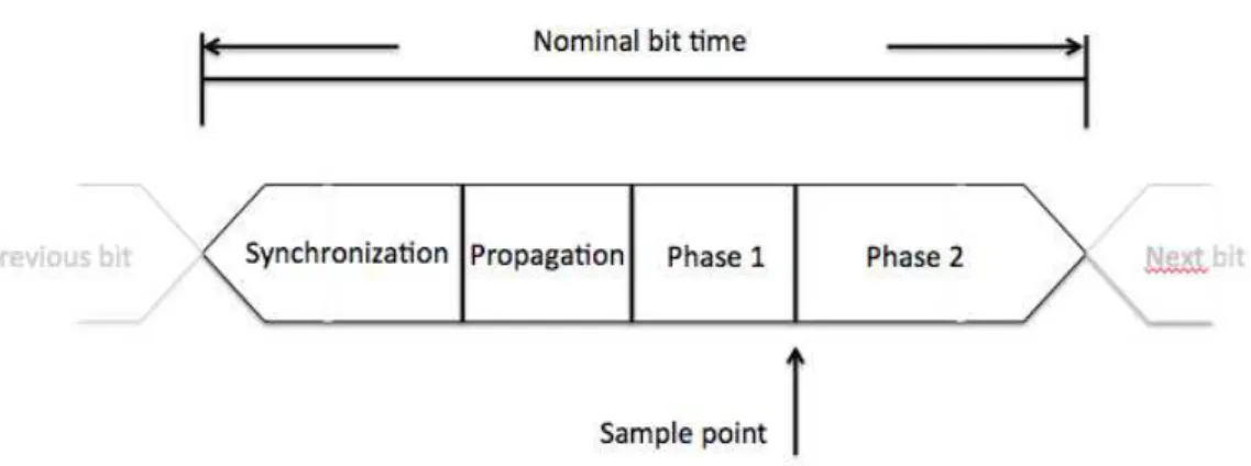
In CAN, every bit itself is divided in to several sub-parts. Seen in Figure 2.1 there is an overview of one bit in CAN. The length of these sub-parts are determined by a time quantum. Time quantum is determined through Equation (2.2), where M is is the value of the prescaler, where minimum time quantum is just a starting point.
TIME QUANTUM=M*MINIMUM TIME QUANTUM (2.1)
Figure 2.1: Bit timing.
At the synchronisation part, that is the time it take for various node on the bus to synchronise, also an overshoot is expected here.
2.6
Analysis techniques
Data analysis is a process of inspecting and transforming data with the objective to discover useful information, suggestions for conclusions and support trouble-shooting. How one chooses to analyze a analog signal will have a significant ef-fect on the results. If a signal is under-sampled, peaks will be unnoticed and for instance a peak-to-peak value, will not be accurate. Moreover will the chosen meth-ods sometimes show and indicate different outcomes. Outcomes and results in terms of possible reasons for the shown error.
2.6.1
Measuring quality
Quality has two aspects in this project. First there is the quality of the measure-ment, how well the data is measured. Second is the quality of the data. Data is not equal to measurement and will always differ in a minimized uncertainty. How-ever, the quality of the measurement is determined through the analog hardware components, how the signal is shifted and amplified and possibly interfered on the board, and the sampling of the ADC. However, the quality of the data is the quality aspect this project targets to value which would represent all the disturbances and interferences arising on the CAN-bus.
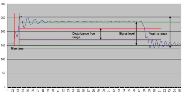
Quality is in many ways rather subjectively defined. The quality of this analogue signal will be determined through three different measurements, all weighted equally, that is the edge steepness, the disturbance free voltage and reflections. Each anal-ysis methods and its definition is shown in the Figure 2.2, where the x avis are the amount of samples and y-axis is the resolution of 8-bit.
Theory 19
Figure 2.2: Overview of analyze methods for a single emulated CAN-bit signal.
2.6.2
Edge steepness
Edge steepness is measured through calculating the rise time for when the logical 0 becomes a logical 1. This is defined as 10 percent more of the value for where the signal just starts to increase, for instance if it is 10 the value ’x’ is 11, i.e. 10 percent more. However, the maximum value for where the signal starts to decrease to its steady state, is multiplied with a factor 0.9, i.e. 10 percent less than its original signal making a maximum value of 20 become effectively 18. However, this would give us a difference of 7, which is defined as the rise time of a signal.
However, in the quality aspect, this value itself has to be put against some opti-mum value of rise time versus a worst case scenario value. Hence, the bit time will be taken in consideration. Each bit is sampled a certain amount of times, so obvi-ously one has to compute the analysis for one bit logical ’1’. The times each bit are sampled set the way the rise time is determined. In the test bench of this project, one bit includes different amount samples of data due to the different baudrates. Hence, the edge steepness worst rise time is when 100 samples have passed to the maximum value is found. which gives the equation of edge steepness in percentage as (100-rise time)/100. However, the sought adapting system description would be:
Percentage=
Amount of samples
2 (perbit)−rise time
Amount of samples
2 (perbit)
(2.2)
2.6.3
Disturbance-free voltage
Disturbance free voltage is measured through comparing the amount of free space between the signals’ worst oscillation. Basically it is the voltage where no oscillations occur. This value is weighted and calculated in relation to the signal level, that is in a optimum square-wave output, which means no rise-time and no oscillation. This means that 0% quality measurement is almost impossible, because then the disturbance free voltage will be 0 and there will be no visual waves, or just high oscillations.
2.6.4
Reflection
Reflection is measured as the ratio between the Disturbance-free voltage and the peak-to-peak value, where peak-to-peak is the maximum and minimum value of a bit.
2.6.5
CAN controller output vs analogue
The digital information is used to control which node in the distributed CAN network that had the quality displayed through the analyze measurements. It connects the analog data, to the node on the network.
Market analysis
In this section a market analysis will be described for which several similar products found are examined in order to evaluate the criteria for the analyzer made in this project, to view what techniques that are already used and the price setting of them. The market analysis was conducted through searches on the internet accordingly to Section 1.4.6. Products most similar to the requirements of this project have been searched for.
3.1
CAN-bus tester 2
CAN-bus tester 2 (CBT2) is a universal diagnosis tool for the CAN bus, in terms of monitoring, troubleshooting, analysing quality of the signal, looking for faults. Typical errors that occur during transmission can be detected through this tool and according to the developer of CAN-bus tester 2 there are often physical layer issues that supply the reason for several common faults in a CAN network. CBT2 is found marketed both by IXXAT and GEMAC brands, however IXXAT is one of GEMACs’ distributors and the manual is GEMACs’.
Functional features:
• Monitor, troubleshoots the CAN bus traffic both sending and receiving • Automatically detects and adjusts to the networks baud rate
• Automatically finds the nodes on the network
• Supports CAN, CANopen, DeviceNet and SAE J1939
Software features:
• Measure quality, edge steepness, disturbance free voltage and reflection of the
analogue part
• Connect quality measurement of the analogue signal to the digital signal and
its node
• Detects transmission line mismatches
• Real-time monitoring of CAN signals, bus status, etc, on the computer • A built-in digital oscilloscope of the frames being sent
Functional description:
The manual states that the CBT2 has a sample rate of approximately 64 MS/s due to its sampling of each bit 64 times and having a bit rate of 1 Mbit/s. The module uses a general quality aspect of the analogue signal, evaluating measurements of the edge steepness, disturbance free voltage, signal level, overshoot and reflection. It weight three measurement of disturbance-free voltage in relation to a perfect CAN voltage reference, as well with the reflection and edge steepness. Those are compared to a value that is ”seen” to be a 100 percent quality level respectively 0 percent. Those three measurements are weighted equally to a general quality measurement giving in the spectrum 0-100 %.
Observed weaknesses:
All the functionality is based on examination and troubleshooting with a computer. It is also necessary to have the right knowledge about CAN in order to fully under-stand the product’s analysis. Moreover the price is rather high, more than 30 times the price of CAN bus analyzer that at least has the functionality of monitoring and transmission of the CAN messages.
Some comments on the way to measure the signal quality is that those concepts don’t reflect all possible ways to determine the signal quality. Measurements such as overshoot and undershoot is interesting as an example.
Price and availability:
CBT2 is sold at IXXATs’ web shope for 5700 USD and according to the manual it is also necessary to have the additional licences purchased in order to use CANopen, DeviceNet or SAEJ1939. [8]
Market analysis 23
3.2
CAN BUS Analyzer Tool
The CAN bus analyzer is intended to be a easy-usage low cost CAN message mon-itor made and primarily sold by Microchip. It supports CAN 2.0B and high-speed CAN with transmission rates up to 1 Mbit/s. It can be used to monitor and debug a CAN network with a graphical user interface.
Features:
• Mini USB connector
• Status,trigger,error and transmission LEDs
• Access to the CAN high,low, RX and TX pins through a screw terminal. • DB9 connector for the CAN BUS.
Software features:
• Monitor the CAN bus traffic • Transmit single shots onto the bus
• Transmit a list of CAN messages in order to the bus • Configure visibility on the trace window of each message • Save CAN bus traffic
Functional description:
The user interface can be used to transmit and receive messages in various form of a rolling window, filtering on ID, DLC or Data. There is also given an appendix with troubleshooting messages that the CAN bus analyzer gives the user. For instance, an error number 1.00.x would say that there is a trouble reading the USB firmware version or 3.20.x states that the data field is empty.
Observed weaknesses:
the signal. The module seems to be used more as a logging tool and can be used as a test node to test the behaviour of the CAN bus and all that is connected, trou-bleshooting the messages being sent, i.e. the digital interpretation from each node CAN controller.
Price and availability
The module is sold on microships’ website for 99.99 USD. It can also be found on RS electronics website for 950 SEK.[9]
3.3
CANwatch
CANwatch is an easy-usage analyzer tool for recognition of errors in a CAN network with display LEDs manufactured and sold by EMS Thomas Wuensche There is no need for specific CAN knowledge in order to use this product, which is mainly because it only analyzes the analogue signal quality of messages being sent on the CAN line. Features:
• Mini USB Connector
• Status, trigger,error and transmission LEDs
• Access to the CAN high,low, RX and TX pins through a screw terminal. • DB9 connector for the CAN bus.
• Fast recognition of errors
• Scanning the analogue signal and evaluating signal quality
Functional description:
CANwatch analyzes the CAN network through only the analog signals’ shape such as overshoot, invalid levels, slow edge steepness and short circuits within the signal line in a digital signal processor. It is sampled at a frequency of 16 Mhz with a 8-bit resolution. Simply working as a node in the CAN network, the CANwatch is connected in the line of the CAN bus or, primarily used for the overall signal quality of a network.
Market analysis 25
Observed weaknesses:
In a bigger CAN network, this module wouldn’t help the user anything in trou-bleshooting more than giving an indication on the general health of the CAN net-work. Due to the neglected analysis of the digital signal, CANwatch can not predict which node that contributes with a bad signal quality.
Price and availability
CANwatch can be ordered directly from EMS Dr. Thomas Wuensches either a hand held or a racked mounted version. On the website, there is no specifed price.[7]
3.4
Summary market analysis
Following Table 4.1 is a comparison of the described products found on the market, this will later be used as a comparison with the results from this thesis and the existing products on the market.
Table 3.1: Market analysis comparison
Functionality CAN-bus tester 2 CAN BUS Analyzer Tool CANwatch Userinterface in computer x x x
Userinterface without computer
Indicating LEDS for troubleshooting x
Analogue analysis of the signal x x
Digital controller to find ID x x
8-bit resolution sampling x
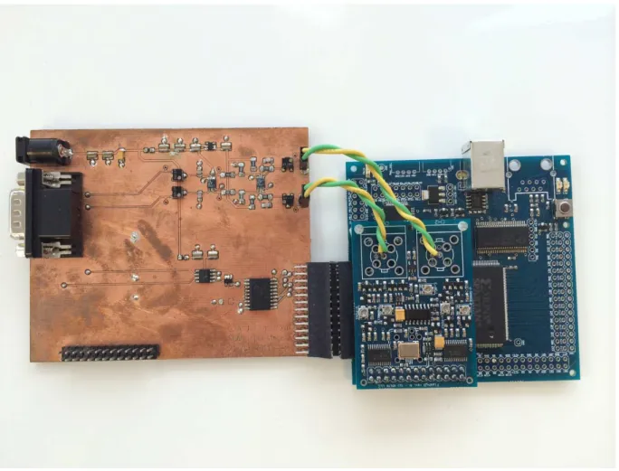
In this section all the hardware tools that the platform are being developed on will be explained. In Figure 4.1 is the real equipment used, seen to the left of the picture is the interface board created by an earlier thesis.
Figure 4.1: Picture of hardware board
4.1
Interface board
Figure 4.2 shows a general overview of the existing interface board.
Hardware and tools 27
Figure 4.2: Overview of existing interface hardware
4.1.1
Power supply
The interface board operates on a 5 V wall wart adapter and includes several filtering and decoupling stages in order to make sure that a stable power is delivered to the components on the board. The power to the analogue and the digital components is divided in order to avoid noise from the other components.
The interface board also contains an ADR130 voltage reference to provide a 0.5 V voltage to the operational amplifier in the signal conditioning circuit.
4.1.2
Signal conditioning
The signal conditioning network strives to match the ADC board’s input range. It filters, shifts and scales the analogue CAN signals to range 0 to 1 V. Basically the network begins with a impedance increasing voltage follower and then a simple two resistance voltage divider followed by a shifting circuit, built upon the same operational amplifiers as the first voltage follower, but this is fed on the inverting input with a 0.5 V signal. It has a feedback circuit of a resistor and a capacitor
in order to match the range of 0-1 V output and collateral stability. This network board is developed by a previous thesis.
4.1.3
Digital CAN interface
The CAN interface consists of two major components, a CAN transceiver and a con-troller. The CAN controller is a chip, MCP2515, that implements the CAN version 2.0B which makes it compatible with 2.0A as well and is hence capable of receiving and transmitting both standard and extended data frames and remote frames. The MCP2515 consists of mainly three blocks; the CAN module which handles the CAN protocol engine, receives and transmits buffers, filters and masks, the control logic that initializes and configures the device, and the interface with microcontrollers through a standard SPI interface.
The CAN module handles all the functions for receiving and transmitting messages. When a message is being received, the message is checked for errors by reading appropriate registers, and will be removed if the user-defined is initialized in that manner, or moved into one of the two received buffers. The Transmitting proce-dure works basically the other way around by first loading the appropriate message buffer and control register to make sure that the message is defined correctly and not a incomplete message is to be transmitted, and furthermore the transmission is initiated by using control register bits via the SPI interface.
The control logic module controls the setup and the operation by interfacing to the other blocks, passing information and control. It is connected to several pins, including ones used for interrupt. This in order to check if a message has been received correctly in to a buffer or for example that a transmission is initiated. [10]
4.2
Flashy-D
The FlashyD board is a 3.3 V powered 8-bit sampling ADC module, commonly used to create a digital oscilloscope. On the board is two ADC08200 which is a low power, 8 bit single input ADC. It is designed to work between 20 - 200 MS/s and has a 44
Hardware and tools 29 dB Signal-to-Noise Ratio (SNR). The device uses a technique that achieves over 7 effective bits at input frequencies up to and even beyond 100 Mhz. Data is acquired at every rising edge of the clock and as long as the clock is present and the ”power down” pin is low, the module will constantly digitize data.
The board also consists of a switched capacitor bandgap which makes the ADC08200 have a power consumption that is proportional to the frequency so that it limits he power to the clock rate utilized.[11]
4.3
Xylo-LM FPGA
Xylo-LM is a development board for FPGA and microcontroller projects. The board includes a Xilinx Spartan 3E FPGA, an ARM7 processor, an USB controller, and circuitry for driving and controlling those components. The FPGA is configured through the USB link but can also be booted through an EEPROM on the board. [12]
4.3.1
Cypress FX2
The USB controller is a cypress EZ-USB FX2LP. It is a single chip low power USB 2.0 microcontroller which has full configurable general purpose interface. Henceforth the module is termed as ’Cypress FX2’. The Cypress FX2 has a master/slave con-figuration working with either a 8-bit or 16-bit wide bidirectional data bus, however in this project it is used with a 8-bit wide data bus and the USB controller in slave setting and the FPGA as master.[13]
4.3.2
Xilinx Spartan 3E FPGA
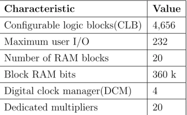
The Spartan 3E field-programmable gate array builds on the earlier Spartan-3 family by mainly increasing the amount of logic per I/O. The Spartan 3E is ideally suited for a wide range of consumer electronics as of this project. It is built on 90 nm process technology. Important characteristics of Spartan 3E that will be in consideration during this project are found in Table 4.1 [14]
Table 4.1: Characterstics of Spartan 3E.
Characteristic Value
Configurable logic blocks(CLB) 4,656
Maximum user I/O 232
Number of RAM blocks 20
Block RAM bits 360 k
Digital clock manager(DCM) 4 Dedicated multipliers 20
4.4
LCD screen KNJN
The LCD screen is a monochrome display, 480x320 pixels with an included adapter board including an EPM3032A PLC. According to distributor of the LCD screen is all logic to control the LCD made on the FPGA. The LCD screen is controlled by on data pin, a clk pin, ground and Vcc. The reference design included by the product was obsolete. No user-guide was included. Seen in Figure 4.3 is the development hardware.
Hardware and tools 31
In this section the implementation steps of this project purposes will be explained. It will use empirical tested data together with theory in order to develop the system required. The text will try to explain how and what is going to be implemented, what has been implemented and what the appearance of the result should be.
5.1
Overview of functionality
The objective to realize the purpose of this study is, to analyze the signal quality, and relate quality to digital interpreted messages at the CAN controller.
The signal sent from the CAN-bus is shifted and amplified in order to have the specified range of voltage defined by the ADC. The sampled data is then sent to the FPGA for signal processing. The FPGA will process the signal by the analysis techniques found in Section 2.6. The analyze result will be evaluated on the FPGA. This is the very foundation of the system and it is adhered functionality additionally to this that will create different systems. The project has several objectives that are sought to be met, hence the functionality of the analyzer will be different systems in terms of code produced. The systems will be developed consecutively, System 1 first, when it works, System 2 and lastly System 3, in this way those systems is more seen as a development process and subgoal.
5.1.1
System 1 - Analogue analyzer
System 1 is a computer to machine working analyzer. It will analyze the analogue signal’s quality, which includes the USB interface code for FPGA to computer, FPGA communication, analyzer and the ADC sampling and computer host script. The result will be shown on the computer as a percentage in the command prompt.
Implementation 33
5.1.2
System 2 - Analogue and digital analyzer
This is where the analysis of the digital data comes into consideration. The system should perform as the previous system with the addition that it should interpret the identifier data and present the quality measurement in relation to the digital data. This should be presented on the command prompt with a communication link that makes the user able to choose what data that should be shown. For example, the user can choose to only see the sampled ADC data, or see the analyzed data and the message id to the message analyzed.
5.1.3
System 3 - User interface
System 3 is to completely take System 1 and 2 and present the information on a LCD graphic display. All the analysis will be presented as fast as the analyser has done it and send it to the LCD.
5.2
Setup test-bench
To create and implement the systems there are some major first steps that have to be taken during the process. One of them is to create a test bench where it is easy creating an emulated CAN signal, and that it is user-friendly to measure the signal and that it doesn’t take to long to setup for a demonstration.
The test-bench should pose a foundation for all systems. However, as System 3 is in many parts, built on System 1 and 2, the evaluation will be done on the PC through a script analyzing data from the FPGA interfacing via an USB.
5.2.1
Added hardware
Some of the hardware needed to be revised in order to get the test bench working properly. One major step has been to utilize a proper terminated cable, so this cable was built in order to get the signal ground normally in the test bench. Also one
operational amplifier didn’t work on the interface board properly and had a shortcut between inverting and non-inverting line but this was fixed.
5.2.2
FPGA logic
On the code implemented on the FPGA, there are mainly 4 blocks or modules. These are a FIFO memory, USB Interface, Interpretator and an ADC Interface. The major design has been with a reference to a clock, building up some processes in VHDL and some different states. Every state is controlled by the clocks but, however, some of the processes happen simultaneously, which means that as soon as any signal in its body or ”sensitivity list” is changed, the process and action is updated. This ba-sically makes the design partly dependent on the clock, but also some simultaneously. A sum up of the entire test-bench, is exemplified through Figure 5.1 with the main signals.
Implementation 35 The chosen design is based on a FIFO memory block to keep track. It is triggered to start its saving on a falling edge of the sampled data from the ADC. The acquired samples from the ADC are stored at a speed of 100 Mhz. However, from the FIFO the samples are read at a speed of 24 Mhz. The FIFO fills up quite fast but has a depth on 16384 bytes and a width of 8 bit and a pre-stored output value of 0x66 to secure any output mistakes.
The USB interface is built to interface with the Cypress FX2 module with the bits for reading, writing, enabling, full, empty and data in/out bus. It has a 8-bit data link for which data is both sent through and received. The module implemented basically reads the data sent from the PC via the data bus, it examines the action and sets some control bits and then sends it to the interpretator. It is also the interface for all transmission from the FPGA to the computer, i.e. all the data from the ADC. Those are only let through on some certain conditions that endorse and make sure that the data sampled is the correct data.
The interpretator does all the bit setting for controlling the internal flow. This means that it decides whether or not the data should be read from the FIFO mod-ules and hence erased from it. It has the functionality to interpret the data from the USB, the command, and set the readenable to the ADC FIFO, if that is requested. The ADC interface is basically just connected to the Flashy-D breakout board for the ADC08200. The ADC module just connects the incoming data from the ADC to the ADC FIFO when a trigger from the ADC values is set, indicating that a CAN message is being received and under condition that the FIFO doesn’t contain any data and stops as soon the FIFO is full.
5.2.3
PC software
The program that runs on the computer for the test bench has basically one purpose, and that is to initiate the right requested transmission through sending it via the USB. However, more functionality is added to the software test-bench to be able to evaluate the data in the best manner possible. For this, the functionality of analyzing the complete data package of the analogue data has been implemented in C++ code.
So not only can the test-bench request data from the FPGAs sampled analogue ADC input, but can also analyze it as a comparison for further development on the FPGA. In C++ it is much easier to compile and test the functionality of an algorithm and the program. For that, mathematical calculations are more simply developed and tested, for instance calculating the rise time, disturbance free voltage and reflec-tion. The entire extracted data can be handled through a dynamic array, saved into it and then stepped through by algorithms to compute the requested calculations. The program starts by setting a register for an USBdevice object, opening and searching for the specific device connected to the computer. It creates an USBde-vice object from which it reads and writes data. The program starts by executing an incoming request, asking the user to ask the FPGA for some data through a command window. In the test bench case, it is a simple letter ’A’ that is required for initiating transmission and calculation. ’A’ stands for the ADC sampling and initiates ADC sampling on the FPGA. Of course will this user interface be more user-narrowed in a further development tool, but as a test bench it includes all the general functionality needed as a foundation to create extra functionality built on this.
As soon the proper command has been written in the command window, the pro-gram calculates through several different functions: the rise-time, the disturbance free voltage, the signal level, the reflection and furthermore a general quality mea-surement based on those functions. How those meamea-surements are specified is found in Section 2.6.
Implementation 37
5.3
System 1 - Analogue analyzer
When the test bench was working properly, functioning the sampled ADC data and displaying it in new made plain text file, the development of the analogue analyzer was started. The program needed some small changes from the test bench idea, but mainly just some additional modules in the FPGA firmware.
The analogue analyzer is based on a program running on the computer, convert-ing known USB data to CAN frames to the FPGA module, in order to emulate the signal. The data is further processed on the FPGA and, when requested, sent back to the PC for a result show.
5.3.1
Emulating CAN-signal
In order to send data in to the FPGA at different bit rates and to have a stable connection, a software program was developed. This program sends data to the USB port into the CANUSB module that converts USB data in to CAN messages. The program on the computer sends a standard CAN frame(11 bit). However, at first there are some setups. All setups ends with [CR], that is ascii 13, for showing the end of the message. At first, the USB port opens through sending the letter O. The desired bit rate is sent to the USB port through the command of Sx, where x is between 0 and 8 seen in Table 5.1.
Table 5.1: Bit rates
Chosen message Bit-rate
0 10 kbit/s 1 20 kbit/s 2 50 kbit/s 3 100 kbit/s 4 125 kbit/s 5 250 kbit/s 6 500 kbit/s 7 800 kbit/s 8 1 Mbit/s
The message is sent by an identifier in hex(000-7FF) followed by the amount of data bytes(0-8) and then the byte value(00-FF). A typical message sent to the CANUSB module could look like: t10021133[CR], t is initiating the transmission. This message is with the identifier 100 and 2 bytes of data that is 11 33.[15] The port closes by sending the command CR. In Figure the interface form is shown.
Implementation 39
5.3.2
FPGA logic
In addition to the logic implemented in the test bench, the analogue analyzer has more advanced ADC interface to filter disturbances and an entire analyze module respectively a FIFO memory to it. It also has a divider IP core implemented. The system is shown in Figure 5.3.
Figure 5.3: System 1 overview of embedded functionality in the FPGA
In order to get all the sampling data saved somehow, regardless of the speed the CAN bus was sending at, a calibration algorithm was developed. This is embedded in the ADC module interface and by a external push of a button, the user of the analyzer can force the analyzer to not sample so often, in order to fill the FIFO memory with an entire message and not just a half. This algorithm is based on the knowledge of the ADC sampling at 133 Mhz and through counting the amount of samples per bit. By doing so, the amount of samples per bit range between 133 samples per bit on a 1 Mbit/s bit-rate, down to 1064 samples per bit with a 125 kbit/s bit-rate. A message length can also vary depending on the amount of data that is being sent. However, the design asserts that at least one entire message is being saved in the modules’ respectively FIFO. The modulation of the sampling rate is done by division of the writing clock to the ADC FIFO giving the functionality to basically jump over some values that have been sampled in the saving process. However, this is only in order to receive a fully received package from the ADC
module, the analyzer doesn’t utilize this functionality.
Moreover the main development in this system was to develop the analyzing al-gorithm, to find the necessary values to be able to use the analyze techniques in Section 2.6. However, the analyzing block did need the idea of a perfectly timed triggered data from the ADC, asserting that it was an entire bit that was to be analyzed. This was done in the ADC interface module, timing the analyze module to only get data when a new bit was coming. However there could be several bits in a row, but it doesn’t matter because the values interesting in investigating in are found right after the first positive edge and right after the negative edge of the bit. The major functionality for the analyzer module is to find four different values in a signal, in order to determine the analyze techniques. The module starts by looking for a new maximum value and when the highest value is found, the value is saved as a new maximum and the local maximum is searched for. Due to the oscillations, the local maximum of the disturbance free range has been empirically proved to be found right after the maximum value. This is graphically shown in Figure 5.4.
Figure 5.4: Analyze values
The maximum value is found as marked with a marker 1 in the Figure 5.4, the minimum value 2 the local disturbance free range maximum. As seen in the figure
Implementation 41 the signal level is between those two values.
As soon as the values start to decrease more rapidly, the minimum value is searched for. When the minimum is found, as the local disturbance free range maximum is found, the next peak after the minimum, seen in Figure 5.4 as value number 4 is the local lowest disturbance free range value. Through these values the peak-to-peak value, disturbance free range, signal level and also the rise-time can be determined. The rise-time is however not ideally calculated. It is determined by actually count-ing the amount of times a new maximum is found. This is how it works: when the analysing module starts, it is certain that the data-flow is in a low-state, i.e. not rising or falling. As soon as the values starts increasing more rapidly, the amount of samples are counted until the first value decreasing from the previous comes. Hence, the value given from the analyzer is more of a guideline for the true rise-time value due to the neglection of the 10 and 90 percentage intervals.
5.3.3
PC software
The major addition in contrast to the test-bench is the calculation of the different measurements. Those are sent from the FPGA to the PC as values as these four points in Figure 5.4 plus the rise-time. In order to present the values as described in Section 2.6, with a quality measurement and certain percentages, several dividing rings needed to be done and those were much easier implemented with the language C++ than straight on the FPGA, mainly because the FPGA could only send an 8-bit message through the USB to the FPGA, representing only integers.
Moreover, small changes with the sending lengths to the FPGA via the USBde-vice were necessary, as well as the choices for requested data. This time, the letter ’B’ stood for requesting the analyzed data from the FPGA.
5.4
System 2 - Analogue and digital analyzer
Built on the same system as System 1, the interpretation of the digital spectra of the CAN signal could be added on the FPGA logic by three modules: the CAN interface, SPI transceiver and a responding FIFO memory module. The emulation of the CAN signal was done in the same way as System 1.
5.4.1
FPGA logic
In order to communicate with the CAN controller, a SPI transceiver between the FPGA and the controller needed to be implemented. The CAN controller initiates the data frame and generates the clock signal for the SPI interface to control the data in and out from the FPGA.
The major part of the development was to set the controllers’ registers correctly for receiving the CAN-bus messages in a proper way. Several registers were writ-ten to. The RXB0CTRL register decided for the controller how it should trigger on messages being received and where to save it. It was decided to trigger on any message, regardless if it had extended identifier or standard, SOF bit or not. The BFPCTRL register set that one of the pins will be used when a complete message is loaded into one of the buffers, as an interrupt pin.
In order to synchronize and to be able to interpret messages at any nodes, all nodes have to have the same nominal bit rate, i.e. the length of a bit, in a time perspective. And as described in Section 2.5 and seen in Figure 2.1, the nominal bit time is built on a synchronization part, a propagation part, phase 1 and phase 2. Those states have to be decided for the CAN controller in respect to aT Q.
The synchronization width is set to 1 timesT Qand the baud-rate prescaler (BRP) to 0, giving Equation (5.1).
TQ= 2∗BRP + 1 Fosc
Implementation 43 TQ= 2 6∗106 = 10 3 ∗10 −7s (5.2)
The bus line is sampled one time with a normal sample point, and the phase 1 is 5∗T Q with a propagation of 2∗T Q and a phase 2 of 4∗T Q. This gives a total
bit-time of 12∗T Q which is 40∗10−7 s. Those setups are set accordingly to the
datasheet [10] and for a high bit-rate of 1 Mbit/s. Any lower bit-rate will make it hard to interpret each bit and under 800 kbit/s it won’t work with this static design and hence it is necessary for the FPGA to sense the baud rate before this value is set.
5.4.2
PC software
The additional software was only a new command for requesting the data from the CAN controllers FIFO memory and read it as a hexadecimal digit and save it to the .txt file.
5.5
System 3 - User interface
The LCD screen should show the information as soon as it was processed by the FPGA through typical letters and numbers. The first objective with controlling the LCD was thus to create a character generator, and create two embedded RAM mem-ory. One that holds all the characters information for the LCD screen to ”show” one of them, and one RAM that pointed to the right information in the character RAM memory in order to send request through a 8-bit value that pointed to that particular ascii representation.
However, the LCD screen was bought in consideration of time restraints and that HDL reference design was attached to the product. Unfortunately, the reference de-sign couldn’t be used at all and a deep e-mail conversation with the sales responsible ended with no user-guides nor nothing of how to control the LCD.
Results and verification
This section contains the results and the verification of the project findings and solutions. It includes measurements of various subsystems in the development of the project. The section tries to emphasize the validity of the results and pose the foundation for further analysis.
6.1
General discussion results
The result and verification measurements are done in a laboratory environment during different periods of the development process. The measurement setups have been connected with an oscilloscope to secure the information processed.
6.2
Test-bench result
Figure 6.1 shows the prompt application with the first step in the send procedure, a letter ’A’ for requesting the sampled ADC data and automatically doing a analysis of the data on the computer.
Figure 6.1: First request command.
Figure 6.2 shows the example of writing a 8-bit value (letter ’A’) to the FPGA which acts as a request for the FPGA to mirror the message and send it back to the computer in the data out bus.
Figure 6.2: Requesting a mirrored send package from the FPGA by sending a
8-bit value.
This was the very foundation for the bidirectional communication between PC and FPGA. Figure 6.3 shows the results of the sampled ADC data and associated signal analysis as described in Section 5.2.
Figure 6.3: ADC data written to a text file and shown in excel.
Results and verification 47 However, the test-bench system was developed with a different emulator of the CAN-signal and when the interface board still was shorted on theCAN H signal. As this problem was solved along the way of development, no more verification is done on this functionality. Nevertheless, in the following systems, both the ADC data and the analysed sequence will be verified.
6.3
System 1 - Analogue analyzer
Seen in Figure 6.5 is the user interface of the analyzer, in command prompt. The result of an analysis of the first message is shown accordingly to the analysis Section 2.6.
Figure 6.5: Result of an analysis for system 1.
In Figure 6.6 is the verification of the maximum, minimum, local maximum and local minimum value found. These values are from textfile, written from the ’A’ letter that was sent to the FPGA, requesting the ADC data followed by the analysis request.
[Max and local max value.] [Min and local min value.]
Figure 6.6: Verified analysis maximum value, minimum value and local
maxi-mum and minimaxi-mum as the marks seen in Figure 5.4.
The rise-time is found to be 30 ns due to that the first peak is found after just three samples, seen in Figure 6.7. At a sampling ratio of 100 Mhz, three samples represent 30ns rise-time.
Figure 6.7: Rise-time ADC values.
6.4
System 2 - Analogue and digital analyzer
In Figure 6.8 is both an analogue analysis of the signal quality, the message ID and data is also digital interpreted and verified to be the very message that was sent.