1
Fundamentals of Scanning
Electron Microscopy
Weilie Zhou, Robert P. Apkarian, Zhong Lin Wang, and David Joy
1
1. Introduction
The scanning electron microscope (SEM) is one of the most versatile instruments available for the examination and analysis of the microstructure morphology and chemical composition characterizations. It is necessary to know the basic princi-ples of light optics in order to understand the fundamentals of electron microscopy. The unaided eye can discriminate objects subtending about 1/60˚ visual angle, cor-responding to a resolution of ~0.1 mm (at the optimum viewing distance of 25 cm). Optical microscopy has the limit of resolution of ~2,000 Å by enlarging the visual angle through optical lens. Light microscopy has been, and continues to be, of great importance to scientific research. Since the discovery that electrons can be deflected by the magnetic field in numerous experiments in the 1890s [1], electron microscopy has been developed by replacing the light source with high-energy electron beam. In this section, we will, for a split second, go over the the-oretical basics of scanning electron microscopy including the resolution limitation, electron beam interactions with specimens, and signal generation.
1.1. Resolution and Abbe’s Equation
The limit of resolution is defined as the minimum distances by which two struc-tures can be separated and still appear as two distinct objects. Ernst Abbe [1] proved that the limit of resolution depends on the wavelength of the illumination source. At certain wavelength, when resolution exceeds the limit, the magnified image blurs.
Because of diffraction and interference, a point of light cannot be focused as a perfect dot. Instead, the image will have the appearance of a larger diameter than the source, consisting of a disk composed of concentric circles with diminishing intensity. This is known as an Airy disk and is represented in Fig. 1.1a. The pri-mary wave front contains approximately 84% of the light energy, and the intensity of secondary and tertiary wave fronts decay rapidly at higher orders. Generally, the radius of Airy disk is defined as the distance between the first-order peak and
the first-order trough, as shown in Fig. 1.1a. When the center of two primary peaks are separated by a distance equal to the radius of Airy disk, the two objects can be distinguished from each other, as shown in Fig. 1.1b. Resolution in a perfect opti-cal system can be described mathematiopti-cally by Abbe’s equation. In this equation:
d=0.612 l/ n sin a
where
d = resolution
l= wavelength of imaging radiation
n = index of refraction of medium between point source and lens, relative to free
space
a= half the angle of the cone of light from specimen plane accepted by the objec-tive (half aperture angle in radians)
n sin αis often called numerical aperture (NA).
Substituting the illumination source and condenser lens with electron beam and electromagnetic coils in light microscopes, respectively, the first transmission electron microscope (TEM) was constructed in the 1930s [2], in which electron beam was focused by an electromagnetic condenser lens onto the specimen plane. The SEM utilizes a focused electron beam to scan across the surface of the spec-imen systematically, producing large numbers of signals, which will be discussed in detail later. These electron signals are eventually converted to a visual signal displayed on a cathode ray tube (CRT).
1.1.1. Interaction of Electron with Samples
Image formation in the SEM is dependent on the acquisition of signals produced from the electron beam and specimen interactions. These interactions can be divided into two major categories: elastic interactions and inelastic interactions.
(a)
(b)
Elastic scattering results from the deflection of the incident electron by the spec-imen atomic nucleus or by outer shell electrons of similar energy. This kind of interaction is characterized by negligible energy loss during the collision and by a wide-angle directional change of the scattered electron. Incident electrons that are elastically scattered through an angle of more than 90˚ are called backscat-tered electrons (BSE), and yield a useful signal for imaging the sample. Inelastic scattering occurs through a variety of interactions between the incident electrons and the electrons and atoms of the sample, and results in the primary beam elec-tron transferring substantial energy to that atom. The amount of energy loss depends on whether the specimen electrons are excited singly or collectively and on the binding energy of the electron to the atom. As a result, the excitation of the specimen electrons during the ionization of specimen atoms leads to the genera-tion of secondary electrons (SE), which are convengenera-tionally defined as possessing energies of less than 50 eV and can be used to image or analyze the sample. In addition to those signals that are utilized to form an image, a number of other signals are produced when an electron beam strikes a sample, including the emis-sion of characteristic x-rays, Auger electrons, and cathodoluminescence. We will discuss these signals in the later sections. Figure 1.2 shows the regions from which different signals are detected.
1 Beam
Backscatterred electrons Secondary electrons Auger electrons
Characteristic x-rays X-ray continuum
FIGURE1.2. Illustration of several signals generated by the electron beam–specimen inter-action in the scanning electron microscope and the regions from which the signals can be detected.
In most cases when incident electron strikes the specimen surface, instead of being bounced off immediately, the energetic electrons penetrate into the sample for some distance before they encounter and collide with a specimen atom. In doing so, the primary electron beam produces what is known as a region of primary excitation, from which a variety of signals are produced. The size and shape of this zone is largely dependent upon the beam electron energy and the atomic number, and hence the density, of the specimen. Figure 1.3 illustrates the variation of interaction volume with respect to different accelerating voltage and atomic number. At certain accelerating voltage, the shape of interaction volume is “tear drop” for low atomic number specimen and hemisphere for specimens of high atomic number. The volume and depth of penetration increase with an increase of the beam energy and fall with the increasing specimen atomic num-ber because specimens with higher atomic numnum-ber have more particles to stop electron penetration. One influence of the interaction volume on signal acquisi-tion is that use of a high accelerating voltage will result in deep penetraacquisi-tion length and a large primary excitation region, and ultimately cause the loss of detailed surface information of the samples. A close-packed opal structure observed by a field emission scanning electron microscope (FESEM) at different accelerating voltages is shown in Fig. 1.4. Images taken under 1 kV gave more surface details than that of 20 kV. The surface resolution is lost at high accelerating voltages and the surface of spheres looks smooth.
1.1.2. Secondary Electrons
The most widely used signal produced by the interaction of the primary electron beam with the specimen is the secondary electron emission signal. When the pri-mary beam strikes the sample surface causing the ionization of specimen atoms,
Lower accelerating Higher accelerating
1 1
(a) (b)
FIGURE1.3. Influence of accelerating voltage and specimen atomic number on the primary
loosely bound electrons may be emitted and these are referred to as secondary electrons. As they have low energy, typically an average of around 3–5 eV, they can only escape from a region within a few nanometers of the material surface. So secondary electrons accurately mark the position of the beam and give topographic information with good resolution. Because of their low energy, secondary elec-trons are readily attracted to a detector carrying some applied bias. The Everhart– Thornley (ET) detector, which is the standard collector for secondary electrons in most SEMs therefore applies both a bias (+10 kV) to the scintillator and a lower bias (+300 V) to the Faraday cage, which screens the detector. In order to detect the secondary electrons a scintillator converts the energy of the electrons into pho-tons (visible light). The phopho-tons then produced travel down a Plexiglas or polished quartz light pipe and move out through the specimen chamber wall, and into a pho-tomultiplier tube (PMT) which converts the quantum energy of the photons back into electrons. The output voltage from the PMT is further amplified before being output as brightness modulation on the display screen of the SEM.
Secondary electrons are used principally for topographic contrast in the SEM, i.e., for the visualization of surface texture and roughness. The topographical image is dependent on how many of the secondary electrons actually reach the detector. A secondary electron signal can resolve surface structures down to the order of 10 nm or better. Although an equivalent number of secondary electrons might be produced as a result of the specimen primary beam interaction, only those that can reach the detector will contribute to the ultimate image. Secondary electrons that are prevented from reaching the detector will generate shadows or be darker in contrast than those regions that have an unobstructed electron path to the detector. It is apparent in the diagram that topography also affects the zone of secondary electron emission. When the specimen surface is perpendicular to the beam, the zone from which secondary electrons are emitted is smaller than found when the surface is tilted. Figure 1.5 illustrates the effect of specimen topography and the position of detector on the secondary electron signals.
(a) (b)
500 nm 500 nm
FIGURE1.4. Scanning electron micrographs of a CaF2close-packed opal structure, which are taken under different accelerating voltages: (a) 1 kV and (b) 20 kV.
Low voltage incident electrons will generate secondary electrons from the very surface region, which will reveal more detailed structure information on the sam-ple surface. More about this will be discussed in Chapter 4.
1.1.3. Backscattered Electrons
Another valuable method of producing an image in SEM is by the detection of BSEs, which provide both compositional and topographic information in the SEM. A BSE is defined as one which has undergone a single or multiple scatter-ing events and which escapes from the surface with an energy greater than 50 eV. The elastic collision between an electron and the specimen atomic nucleus causes the electron to bounce back with wide-angle directional change. Roughly 10–50% of the beam electrons are backscattered toward their source, and on an average these electrons retain 60–80% of their initial energy. Elements with higher atomic numbers have more positive charges on the nucleus, and as a result, more electrons are backscattered, causing the resulting backscattered signal to be higher. Thus, the backscattered yield, defined as the percentage of incident elec-trons that are reemitted by the sample, is dependent upon the atomic number of the sample, providing atomic number contrast in the SEM images. For example, the BSE yield is ~6% for a light element such as carbon, whereas it is ~50% for a heavier element such as tungsten or gold. Due to the fact that BSEs have a large energy, which prevents them from being absorbed by the sample, the region of the specimen from which BSEs are produced is considerably larger than it is for secondary electrons. For this reason the lateral resolution of a BSE image is
Detector
FIGURE1.5. Illustration of effect of surface topography and position of detector on the
considerably worse (1.0 µm) than it is for a secondary electron image (10 nm). But with a fairly large width of escape depth, BSEs carry information about fea-tures that are deep beneath the surface. In examining relatively flat samples, BSEs can be used to produce a topographical image that differs from that produced by secondary electrons, because some BSEs are blocked by regions of the specimen that secondary electrons might be drawn around.
The detector for BSEs differs from that used for secondary electrons in that a biased Faraday cage is not employed to attract the electrons. In fact the Faraday cage is often biased negatively to repel any secondary electrons from reaching the detector. Only those electrons that travel in a straight path from the specimen to the detector go toward forming the backscattered image. Figure 1.6 shows images of Ni/Au heterostructure nanorods. The contrast differences in the image produced by using secondary electron signal are difficult to interpret (Fig. 1.6a), but contrast difference constructed by the BSE signal are easily discriminated (Fig. 1.6b).
The newly developed electron backscattered diffraction (EBSD) technique is able to determine crystal structure of various samples, including nanosized crystals. The details will be discussed in Chapter 2.
1.1.4. Characteristic X-rays
Another class of signals produced by the interaction of the primary electron beam with the specimen is characteristic x-rays. The analysis of characteristic x-rays to provide chemical information is the most widely used microanalytical technique in the SEM. When an inner shell electron is displaced by collision with a primary electron, an outer shell electron may fall into the inner shell to reestablish the proper charge balance in its orbitals following an ionization event. Thus, by the emission of an x-ray photon, the ionized atom returns to ground state. In addition to the characteristic x-ray peaks, a continuous background is generated through the deceleration of high-energy electrons as they interact with the electron cloud
Mag = 10.00 kx3 µm EHT = 5.00 kVWD = 7 mm Photo No. = 3884Signal A= InLens Date :13 Nov 2004Time :16:13:36 Mag = 10.00 kx 1 µm EHT = 19.00 kVWD = 7 mm Signal A = QBSDPhoto No. = 3889 Date :13 Nov 2004Time :16:23:31
(a) (b)
FIGURE 1.6. Ni/Au nanorods images formed by (a) secondary electron signal and (b)
and with the nuclei of atoms in the sample. This component is referred to as the
Bremsstrahlung or Continuum x-ray signal. This constitutes a background noise,
and is usually stripped from the spectrum before analysis although it contains information that is essential to the proper understanding and quantification of the emitted spectrum. More about characteristic x-rays for nanostructure analysis will be discussed in Chapter 3.
1.1.5. Other Electrons
In addition to the most commonly used signals including BSEs, secondary electrons, and characteristic x-rays, there are several other kinds of signals gen-erated during the specimen electron beam interaction, which could be used for microstructure analysis. They are Auger electrons, cathodoluminescence-transmitted electrons and specimen (or absorbed) current.
1.1.5.1. Auger Electrons
Auger electrons are produced following the ionization of an atom by the incident electron beam and the falling back of an outer shell electron to fill an inner shell vacancy. The excess energy released by this process may be carried away by an Auger electron. This electron has a characteristic energy and can therefore be used to provide chemical information. Because of their low energies, Auger elec-trons are emitted only from near the surface. They have escape depths of only a few nanometers and are principally used in surface analysis.
1.1.5.2. Cathodoluminescence
Cathodoluminescence is another mechanism for energy stabilization following beam specimen interaction. Certain materials will release excess energy in the form of photons with infrared, visible, or ultraviolet wavelengths when electrons recombine to fill holes made by the collision of the primary beam with the spec-imen. These photons can be detected and counted by using a light pipe and pho-tomultiplier similar to the ones utilized by the secondary electron detector. The best possible image resolution using this approach is estimated at about 50 nm.
1.1.5.3. Transmitted Electrons
Transmitted electrons is another method that can be used in the SEM to create an image if the specimen is thin enough for primary beam electrons to pass through (usually less than 1 µ). As with the secondary and BSE detectors, the transmitted electron detector is comprised of scintillator, light pipe (or guide), and a photo-multiplier, but it is positioned facing the underside of the specimen (perpendicu-lar to the optical axis of the microscope). This technique allows SEM to examine the internal ultrastructure of thin specimens. Coupled with x-ray microanalysis, transmitted electrons can be used to acquisition of elemental information and dis-tribution. The integration of scanning electron beam with a transmission electron microscopy detector generates scanning transmission electron microscopy, which will be discussed in Chapter 6.
1.1.5.4. Specimen Current
Specimen current is defined as the difference between the primary beam current and the total emissive current (backscattered, secondary, and Auger electrons). Specimens that have stronger emission currents thus will have weaker specimen currents and vice versa. One advantage of specimen current imaging is that the sample is its own detector. There is thus no problem in imaging in this mode with the specimen as close as is desired to the lens.
2. Configuration of Scanning Electron
Microscopes
In this section, we will present a detailed discussion of the major components in an SEM. Figure 1.7 shows a column structure of a conventional SEM. The elec-tron gun, which is on the top of the column, produces the elecelec-trons and acceler-ates them to an energy level of 0.1–30 keV. The diameter of electron beam produced by hairpin tungsten gun is too large to form a high-resolution image. So, electromagnetic lenses and apertures are used to focus and define the electron beam and to form a small focused electron spot on the specimen. This process demagnifies the size of the electron source (~50 µm for a tungsten filament) down to the final required spot size (1–100 nm). A high-vacuum environment, which allows electron travel without scattering by the air, is needed. The specimen stage, electron beam scanning coils, signal detection, and processing system pro-vide real-time observation and image recording of the specimen surface.
2.1. Electron Guns
Modern SEM systems require that the electron gun produces a stable electron beam with high current, small spot size, adjustable energy, and small energy dis-persion. Several types of electron guns are used in SEM system and the qualities of electrons beam they produced vary considerably. The first SEM systems gen-erally used tungsten “hairpin” or lanthanum hexaboride (LaB6) cathodes, but for the modern SEMs, the trend is to use field emission sources, which provide enhanced current and lower energy dispersion. Emitter lifetime is another impor-tant consideration for selection of electron sources.
2.1.1. Tungsten Electron Guns
Tungsten electron guns have been used for more than 70 years, and their reliabil-ity and low cost encourage their use in many applications, especially for low mag-nification imaging and x-ray microanalysis [3]. The most widely used electron gun is composed of three parts: a V-shaped hairpin tungsten filament (the cathode), a Wehnelt cylinder, and an anode, as shown in Fig. 1.8. The tungsten filament is about 100 µm in diameter. The V-shaped filament is heated to a temperature of
more than 2,800 K by applying a filament current ifso that the electrons can escape from the surface of the filament tip. A negative potential, which is varied in the range of 0.1–30 kV, is applied on the tungsten and Wehnelt cylinder by a high volt-age supply. As the anode is grounded, the electric field between the filament and the anode plate extracts and accelerates the electrons toward the anode. In thermionic emission, the electrons have widely spread trajectories from the filament tip. A slightly negative potential between the Wehnelt cylinder and the filament, referred to “bias,” provides steeply curved equipotentials near the aperture of the
Alignment coil CL (condenser lens) CL OL (Objective lens) aperture Specimen chamber Specimen holder Specimen stage Secondary electron detector OL Scan coil Electron gun Anode
FIGURE1.7. Schematic diagram of a scanning electron microscope (JSM—5410, courtesy of JEOL, USA).
Wehnelt cylinder, which produces a crude focusing of electron beam. The focus-ing effect of Wehnelt cylinder on the electron beam is depicted in Fig. 1.8.
The electron emission increases with the filament current. There is some “saturation point” of filament current, at which we have most effective electron emission (i.e., the highest electron emission is obtained by least amount of cur-rent). At saturation electrons are only emitted from the tip of the filament and focused into a tight bundle by the negative accelerating voltage. If the filament current increases further, the electron emission only increases slightly (Fig. 1.9). It is worth mentioning that there is a peak (known as “false peak”) in beam cur-rent not associated with saturation, and this character is diffecur-rent from instrument to instrument, even from filament to another. This false peak is sometimes even greater than the saturation point. Its cause remains unexplained because it is of little practical use, but its presence could be the result of gun geometries during filament heating and the electrostatic creation of the gun’s crossover. Setting the filament to work at the false peak will result in extremely long filament life, but it also deteriorates the stability of the beam. Overheating the filament with cur-rent higher than saturation curcur-rent will reduce the filament life significantly. The burnt-out filament is shown in Fig. 1.10. The spherical melted end of the broken filament due to the overheating is obvious. The filament life is also influenced by the vacuum status and cleanliness of the gun.
High voltage supply _ + Wehnelt cylinder (grid cap) Anode plate Filament ib Bias supply Filament current if Filament heating supply
FIGURE1.8. Schematic of the self-biased thermionic tungsten electron gun. (The effect of the negative bias of the Wehnelt cylinder on the electron trajectory is shown.)
Filament current, if
Beam current,
ib
Saturation point
False peak
FIGURE1.9. Saturation of a tungsten hairpin electron gun. At saturation point, majority of the electrons are emitted from the tip of the filament and form a tight bundle by accelerat-ing voltage.
200 µm
FIGURE1.10. An SEM image of a “blown-out” tungsten filament due to overheating. A spherical melted end is obvious at the broken filament.
2.1.2. Lanthanum Hexaboride Guns
An alternative for tungsten filament is the LaB6filament. This material has a lower work function (2.4 eV) than tungsten (4.5 eV). This means LaB6 can provide stronger emission of electrons at the same heating temperature. Therefore, LaB6 electron guns provide 5 to 10×greater brightness and a longer lifetime compared with conventional tungsten guns [4]. Figure 1.11a shows the emitter of a LaB6 sin-gle crystal 100–200 µm in diameter and 0.5 mm long. The crystal is mounted on a graphite or rhenium support, which does not chemically react with the LaB6and also serves as the resistive heater to elevate the temperature of crystal so that it can emit electrons. There are several advantages for the use of LaB6electron guns. The effective emission area is much smaller than conventional tungsten electron guns, which reduces the spot size of the electron beam. In addition, the electron beam produced by LaB6 electron guns have smaller energy spread, which means a smaller chromatic aberration and higher resolution of SEM images.
LaB6electron source can replace the tungsten electron guns directly in con-ventional SEMs. However, LaB6is readily oxidized at elevated temperatures and the vacuum in gun chamber of conventional electron microscopes is not high enough to avoid contamination on LaB6cathode. This reduces the lifetime of the guns significantly. Figure 1.11b shows the details of a used LaB6crystal, several contamination spots are easily recognized on its surface. To avoid this situation the chamber electron gun must have a vacuum better than 10−8Torr. Generally,
differential pumping of the gun region is needed. 2.1.3. Field Emission Guns
Thermionic sources depend on a high temperature to overcome the work function of the metal so that the electrons can escape from the cathode. Though they are
(a) (b)
1 mm 200mm
FIGURE1.11. (a) SEM image of LaB6electron gun and (b) a higher magnification image,
inexpensive and the requirement of vacuum is relatively low, the disadvantages, such as short lifetime, low brightness, and large energy spread, restrict their appli-cations. For modern electron microscopes, field emission electron guns (FEG) are a good alternative for thermionic electron guns.
In the FEG, a single crystal tungsten wire with very sharp tip, generally pre-pared by electrolytic etching, is used as the electron source. Figure 1.12a and b shows a micrograph of a typical field emission tip and the schematic structure of the FEG. In this system, a strong electric field forms on the finely oriented tip, and the electrons are drawn toward the anodes instead of being boiled up by the filament heating. Two anodes are used in field emission system, depicted in Fig. 1.12c. The voltage V1with a few kilovolts between the tip and the first anode is used to extract the electrons from the tip, and the V0is the accelerating voltage. There are three types of FEGs that are used in the SEM systems [5]. One is the cold field emission (CFE) sources. The “cold field” means the electron sources operate at room temperature. The emission of electrons from the CFE purely depends on the electric field applied between the anodes and the cathode. Although the current of emitted electron beams is very small, a high brightness can still be achieved because of the small electron beam diameter and emission area. An operation known as “flashing” in which the field emission tip is heated to a temperature of more than 2,000 K for a few seconds is needed to clean absorbed gas on the tip. The second class is thermal field emission (TFE) sources, which is operated in elevated temperature. The elevated temperature reduces the absorption of gas molecules and stabilizes the emission of electron beam even when a degraded vacuum occurs. Beside CFE and TFE sources, Schottky emit-ters (SE) sources are also used in modern SEM system. The performances of SE and CFE sources are superior to thermionic sources in the case of brightness, source size, and lifetime. However, SE source is preferred over CFE source because of its higher stability and easier operation. Because the emitting area of SE source is about 100×larger than that of the CFE source, it is capable to deliver more than 50× higher emission current than CFE at a similar energy spread. Further, a larger size of emission source reduces the susceptibility to vibration.
(a) (b) (c) 1 mm 300 µm First anode second anode V0 V1
FIGURE1.12. (a) Field emission source with extreme sharp tip; (b) a higher magnification image; and (c) schematic diagram of a typical field emission electron source. The two anodes work as an electrostatic lens to form electron beams.
Also, electron beam nanolithography needs high emission current to perform a pattern writing, which will be discussed in Chapter 5.
Compared with thermionic sources, CFE provides enhanced electron bright-ness, typically 100×greater than that for a typical tungsten source. It also pos-sesses very low electron energy spread of 0.3 eV, which reduces the chromatic aberration significantly, and can form a probe smaller than 2 nm, which provides much higher resolution for SEM image. However, field emitters must operate under ultrahigh vacuum (better than 10−9Torr) to stabilize the electron emission
and to prevent contamination.
2.2. Electron Lenses
Electron beams can be focused by electrostatic or magnetic field. But electron beam controlled by magnetic field has smaller aberration, so only magnetic field is employed in SEM system. Coils of wire, known as “electromagnets,” are used to produce magnetic field, and the trajectories of the electrons can be adjusted by the current applied on these coils. Even using the magnetic field to focus the elec-tron beam, electromagnetic lenses still work poorly compared with the glass lenses in terms of aberrations. The electron lenses can be used to magnify or demagnify the electron beam diameter, because their strength is variable, which results in a variable focal length. SEM always uses the electron lenses to demag-nify the “image” of the emission source so that a narrow probe can be formed on the surface of the specimen.
2.2.1. Condenser Lenses
The electron beam will diverge after passing through the anode plate from the emission source. By using the condenser lens, the electron beam is converged and collimated into a relatively parallel stream. A magnetic lens generally consists of two rotationally symmetric iron pole pieces in which there is a copper winding providing magnetic field. There is a hole in the center of pole pieces that allows the electron beam to pass through. A lens-gap separates the two pole pieces, at which the magnetic field affects (focuses) the electron beam. The position of the focal point can be controlled by adjusting the condenser lens current. A condenser aperture, generally, is associated with the condenser lens, and the focal point of the electron beam is above the aperture (Fig. 1.13). As appropriate aperture size is chosen, many of the inhomogeneous and scattered electrons are excluded. For modern electron microscopes, a second condenser lens is often used to provide additional control on the electron beam.
2.2.2. Objective Lenses
The electron beam will diverge below the condenser aperture. Objective lenses are used to focus the electron beam into a probe point at the specimen surface and to supply further demagnification. An appropriate choice of lens demagnification
and aperture size results in a reduction of the diameter of electron beam on the specimen surface (spot size), and enhances the image resolution.
Three designs of objective lenses are shown in Fig. 1.14 [5]. The asymmetric pinhole lens (Fig. 1.14a) is the most common objective lens. There is only a small bore on the pole piece, and this keeps the magnetic field within the lens and pro-vides a field-free region above the specimen for detecting the secondary elec-trons. However, this configuration has a large lens aberration. For the symmetric immersion lens (Fig. 1.14b), the specimen is placed inside the lens, which can reduce the focal length significantly. This configuration provides a lowest lens aberration because lens aberration directly scale with the focal length. But the specimen size cannot exceed 5 mm. The Snorkel lens (Fig. 1.14c) produces a strong magnetic field that extends to the specimen. This kind of lens possesses the advantages of the pinhole lens and the immersion lens, combining low lens aber-ration with permission of large specimen. Furthermore, this configuaber-ration can accommodate two secondary electron detectors (the conventional and in-lens detector). The detail detector configurations will be discussed later.
2.3. Column Parameters
It is easy to imagine that spot size and the beam convergence angle α directly relate to the resolution and the depth of focus of the SEM images, but they are influenced by many other parameters such as electron beam energy, lenses
Electron source Condenser lens Electrons excluded Condenser aperture
FIGURE1.13. A diagram showing how the electrons travel through the condenser lens and
condenser aperture. Many of the nonhomogeneous or scattered electrons are excluded by the condenser aperture.
current, aperture size, working distance (WD), and chromatic and achromatic aberration of electron lenses. In this section, several primary parameters that are significant for the image quality will be discussed and a good understanding of all these parameters is needed because these parameters are interdependent. 2.3.1. Aperture
One or more apertures are employed in the column according to different designs of SEM. Apertures are used to exclude scattered electrons and are used to control the spherical aberrations in the final lens. There are two types of aperture: one is at the base of final lens and is known as real aperture; the other type is known as virtual aperture and it is placed in the electron beam at a point above the final lens. The beam shape and the beam edge sharpness are affected by the real aper-ture. The virtual aperture, which limits the electron beam, is found to have the same affect. The real aperture is the conventional type of aperture system and the virtual aperture is found on most modern SEM system. Because the virtual
Beam limiting aperture (virtual) Beam limiting aperture (virtual) Detector Deflection coils (a) (b) (c) Beam limiting aperture (virtual) Detector Detector 2 Detector 1
FIGURE1.14. Objective lens configurations: (a) asymmetric pinhole lens, which has large lens aberration; (b) symmetric immersion lens, in which small specimen can be observed with small lens aberration; and (c) snorkel lens, where the magnetic field extends to the specimen providing small lens aberration on large specimen (Adapted from [5]).
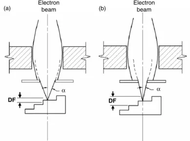
aperture is far away from the specimen chamber it can be kept clean for a long time, but the aperture alignment becomes a regular operation, as its size is very small. Decreasing the aperture size will reduce the beam angle αfor the same WD, resulting in an enhancement of the depth of field (shown in Fig. 1.15) and a decrease of the current in the final probe. Figure 1.16 shows the electron micro-graph of branched grown ZnO nanorods taken with different aperture size. Increase of depth of field due to change of aperture size is easily observed, which is emphasized by circles. An optimum choice of aperture size can also minimize the detrimental effects of aberrations on the probe size [6].
2.3.2. Stigmation
The lens defects (machining errors and asymmetry in lens winding), and con-tamination on aperture or column can cause the cross section of the electron beam profile to vary in shape. Generally, an elliptical cross section is formed instead of a circular one. As a result during operation, the image will stretch along different direction at underfocus and overfocus condition. This imperfection on the elec-tromagnetic lens is called astigmatism. A series of coils surrounding the electron beam, referred to as “stigmator,” can be used to correct astigmatism and achieve an image with higher resolution.
Figure 1.17a shows an SEM image with extreme astigmatism. When moving through focus the image stretches first in one direction (Fig. 1.17b) and when the image is in the in-focus position the stretch is minimized (Fig. 1.17a) before it is stretched to another direction (Fig. 1.17c). The astigmatism correction cycle
DF DF α α Electron beam Electron beam (a) (b)
FIGURE1.15. Small aperture (b) provides enhanced depth of field compared with large
(a) (b)
1 µm 1 µm
FIGURE1.16. Electron micrograph of branch grown ZnO nanorods taken with different aperture sizes: (a) 30 µm and (b) 7.5 µm. The enhancement of depth of field is emphasized by circles.
(c)
(a) (b)
(d)
1 µm
FIGURE 1.17. Comparison of SEM images of opal structure with astigmatism and after
astigmatism correction. (a) SEM image with astigmatism in in-focus condition; (b) SEM image with astigmatism in underfocus condition; (c) SEM image with astigmatism in over-focus condition; and (d) SEM image with astigmatism correction. The inset figures are the schematic diagrams of the shapes of probe spots.
(x-stigmator, focus, y-stigamator, focus) should be repeated, until ultimately the sharpest image is obtained (Fig. 1.17d). At that point the beam cross section will be focused to the smallest point. Generally the compensation for astigmatism is performed while operating at the increased magnification, which ensures the image quality of lower magnification even when perfect compensation is not obtained. However, the astigmatism is not obvious for low magnification observation. 2.3.3. Depth of Field
The portion of the image that appears acceptably in focus is called the “depth of field” [7]. Figure 1.18 shows the effect of a limited depth of field in an SEM image of a SnO2nanojunction sample [8]. Only middle part of the image is in the focus, and the upper side and underside of the image show underfocus and over-focus, respectively. An electron beam with a smaller convergence angle α pro-vides a larger depth of field, because the change of spot size is less significant along the beam direction for a sharper electron beam. Besides the aperture size, the WD will also influence the depth of field, which is demonstrated in Fig. 1.19. At a short WD the sample will be scanned with a wide cone of electrons resulting in an image with little depth of field. By contrast, at a longer WD, corresponding to a narrow cone of electron beam results in an enhanced depth of field. However, a long WD does not mean a high resolution. Depth of field is important when we observe a specimen with large topographical variation. In this case, we prefer to use a long WD so that we can bring as much of the image into focus as possible.
2 µm
But if the topography of the specimen is relatively flat, a shorter WD is preferred as depth of field is less important and higher resolution can be achieved by using a shorter WD. Figure 1.20 is the SEM image of well-aligned Co-doped ZnO nanowire arrays fabricated by a chemical vapor deposition method [9], showing the influence of WD on depth of field. The figures are focused on the middle part of the images. By comparing circled part of the two images, the enhancement of depth of field is obvious by increasing the WD from 3 to 12 mm.
DF α WD DF α WD Electron beam Electron beam (a) (b)
FIGURE1.19. Beam diagram showing enhancement of depth of field (DF) by increasing working distance (WD). (a) Short working distance and (b) long working distance.
(a) (b)
2 µm 2 µm
FIGURE1.20. Well aligned Co-doped ZnO nanowires array fabricated by chemical vapor deposition, showing the enhancement of depth of field by increasing the working distance from (a) 3 mm to (b) 12 mm, which is emphasized by circles.
2.4. Image Formation
Complex interactions occur when the electron beam in an SEM impinges on the specimen surface and excites various signals for SEM observation. The second-ary electrons, BSEs, transmitted electrons, or the specimen current might all be collected and displayed. For gathering the information about the composition of the specimen, the excited x-ray or Auger electrons are analyzed. In this section, we will give a brief introduction about the interactions of the electron beam with the specimen surface and the principle of image formation by different signals.
2.4.1. Signal Generation
The interaction of the electron beam with a specimen occurs within an excitation volume under the specimen surface. The depth of the interaction volume depends on the composition of the solid specimen, the energy of the incident electron beam, and the incident angle. Two kinds of scattering process, the elastic and the inelastic process, are considered. The electrons retain all of their energy after an elastic interaction, and elastic scattering results in the production of BSEs when they travel back to the specimen surface and escape into the vacuum. On the other hand, electrons lose energy in the inelastic scattering process and they excite elec-trons in the specimen lattice. When these low energy elecelec-trons, generally with energy less than 50 eV, escape to the vacuum, they are termed “secondary elec-trons.” Secondary electrons can be excited throughout the interaction volume; however, only those near the specimen surface can escape into the vacuum for their low energy and most of them are absorbed by the specimen atoms. In con-trast, the BSEs can come from greater depths under the specimen surface. In addi-tion to secondary electrons and BSEs, x-rays are excited during the interacaddi-tion of the electron beam with the specimen. There are also several signals that can be used to form the images or analyze the properties of specimen, e.g., Auger electrons, cathodoluminescence, transmitted electrons, and specimen current, which have been discussed in Sections 1.1.5 and 1.1.6.
2.4.2. Scanning Coils
As mentioned in the previous sections, the electron beam is focused into a probe spot on the specimen surface and excites different signals for SEM observation. By recording the magnitude of these signals with suitable detectors, we can obtain information about the specimen properties, e.g., topography and composi-tion. However, this information just comes from one single spot that the electron beam excites. In order to form an image, the probe spot must be moved from place to place by a scanning system. A typical image formation system in the SEM is shown in Fig. 1.21. Scanning coils are used to deflect the electron beam so that it can scan on the specimen surface along x- or y-axis. Several detectors are used to detect different signals: solid state BSE detectors for BSEs; the ET detector for secondary and BSEs; energy-dispersive x-ray spectrometer and
wavelength-dispersive x-ray spectrometer for the characteristic x-rays; and photomultipliers for cathodoluminescence. The details of secondary electron detectors will be discussed in Section 2.4.3. The detected signal is also processed and projected on the CRT screen or camera. The scanning process of CRT or camera is synchronized with the electron beam by the scanning signal generator and hence a point-to-point image for the scanning area is produced.
2.4.3. Secondary Electron Detectors
The original goal in building an SEM was to collect secondary electron images. Because secondary electrons are of low energy they could come only from the surface of the sample under the electron beam and so were expected to provide a rich variety of information about the topography and chemistry of the specimen. However, it did not prove to be an easy task to develop a collection system which could detect a small current (~10−12 A) of low energy electrons at high speed
enough to allow the incident beam to be scanned, and which worked without adding significant noise of its own. The only practical device was the electron multiplier. In this, the secondary electrons from the sample were accelerated onto a cathode where they produced additional secondary electrons that were then in turn accelerated to a second cathode where further signal multiplication occurred. By repeating this process 10 or 20 times, the incident signal was amplified to a large enough level to be used to form the image for display. Although the elec-tron multiplier was in principle sensitive enough, it suffered from the fact that the cathode assemblies were exposed to the pump oil, water vapor, and other con-taminants that were present in the specimen chambers of these early instruments with the result that the sensitivity rapidly degraded unless the multiplier was cleaned after every new sample was inserted.
Scanning coils Final aperture Backscattered electron detector Secondary electron detector Specimen Photomultiplier WDS, EDS Scanning signal generator CRT or camera Signal amplifier
The solution to this problem, and the development that made the SEM a commercial reality, was provided by Everhart and Thornley [10]. Their device consisted of three components: a scintillator that converted the electron signal into light; a light pipe to transfer the light; and a PMT that converts the light sig-nal back into an electron sigsig-nal. Because the amount of light generated by the scintillator depends both on the scintillator material and on the energy of the elec-trons striking it, a bias of typically 10 kV is applied to the scintillator so that every electron strikes it with sufficient energy to generate a significant flash of light. This is then conducted along the light pipe, usually made from quartz or Perspex, toward the PMT. The use of a light pipe makes it possible to position the scintil-lator at the place where it can be most effective in collecting the SE signal while still being able to have the PMT safely away from the sample and stage. Usually the light pipe conducts the light to a window in the vacuum wall of the specimen chamber permitting the PMT to be placed outside the column and vacuum. The conversion of SE first to light and then back to an electron signal makes it possi-ble to use the special properties of the PMT which is a form of an electron mul-tiplier, but is completely sealed and so is not affected by external contaminants. The PMT has a high amplification factor, a logarithmic response which allows it to process signal covering a very large intensity range, is of low noise, responds rapidly to changes in signal level, and is low in price.
This overall arrangement not only offers high efficiency and speed, but is flex-ible in its implementation, is cheap to construct, and needs little routine attention to maintain peak performance. Consequently, it has been present, in one form or another, in every SEM built since that time. The classic form of the ET detector is that shown in Fig. 1.22a where the sample is placed beneath the objective lens
100V–30kV PE Lens
coils
SE = secondary electrons BSE = backscatter electrons
Pole piece SE-IV( 1-4%) SE-III (70%) 1-25% SE-I SE-II BSE BSE Working Distance = 8.50 mm + + + + + ET Detector 12 keV (a)
FIGURE1.22. Three types of different detectors: (a) conventional (below-lens) scanning
of the SEM and the ET detector is positioned to one side. Because of the +10 kV bias on the front face of the scintillator there is an electrostatic field, of the order of a few hundred volts per millimeter, which attracts the SE from the specimen and guides them toward the detector. At low beam energies, however, a field of this magnitude is sufficient to deflect the incident beam off axis, so a Faraday screen in the form of a widely spaced metal grid is often placed over the scintil-lator itself to shield the beam. The Faraday screen itself is biased to just 250 or 300 V positive, which is enough to attract many of the emitted SE, but is too low to deviate the beam.
30kV
Above Lens Detector
Steam Detector ET Detector SE-I SE-I SE-II SE-II SE-II BSE Savgula Holder + ++ ++ (b) On ET Detector SE-I SE-II Near lens Off Sample ET Detector + + + + + (c)
FIGURE1.22. (Continued) (b) condenser/objective (in-lens) scanning electron microscope with above-lens ET detector; and (c) high-resolution (near-lens) scanning electron micro-scope with above-lens ET detector.
Secondary emission from a horizontal specimen is isotropic about the surface normal, and with the maximum intensity being emitted normal to the surface. Experimental measurements [11] show that this form of the ET detector typically collects about 15–30% of the available SE signal. This relatively poor perform-ance is the result of the fact that many of the SE escape through the bore of the lens and travel back up the column, and also because the asymmetric positioning of the detector only favors collection from half of the emitted SE distribution with a velocity component toward detector. In general this performance is quite satis-factory because of the way in which secondary electron images are interpreted [5]. The viewpoint of the operator is effectively looking down along the beam direction onto the specimen, which is being illuminated by light emitted from the detector assembly. An asymmetric detector geometry therefore results in an image in which topography (e.g., edges, corners, steps, and surface roughness) is shadowed or highlighted depending on the relative position of the feature and the detector. This type of image contrast is intuitively easy and reliable to interpret and produces aesthetically pleasing micrographs.
The main drawback with this arrangement, also evident from Fig. 1.22a, is that the detector will be bombarded not only by the SE1 and SE2 secondary electrons from the specimen carrying the desired specimen information, but also by BSEs from the specimen, and by tertiary electrons (SE3) created by BSE impact on the lens and the chamber walls. Typically at least half of the signal into the detector is from direct backscatters or in the form of SE3 generated by scattering in the sample area. As a result the fraction of SE content from the sample is diluted, the signal-to-noise ratio is degraded, and image detail is reduced in contrast. Although for many purposes it is simply sufficient that the detector produces an adequately large signal, for many advanced techniques it is essential that only specific classes of electrons contribute to the image and in those cases this first type of SE is far from optimum.
In basic SEMs the WD is typically of the order of 12–20 mm so the ET detec-tor can readily be positioned close to the specimen and with a good viewpoint above it. In more advanced microscopes, the WD is often much smaller in order to enhance image resolution and locating the detector is therefore more difficult. Such SEMs often employ a unipole or “snorkel” lens configuration, which pro-duces a large magnetic field at the specimen surface. This field captures a large fraction of the SE emission and channels it back through the bore of the lens and up the column. In order to provide efficient SE imaging the arrangement of Fig. 1.22b is therefore often employed. A standard ET detector is provided as before, for occasions when the sample is imaged at a high WD, or for imaging tilted samples. A second detector is provided above the objective lens to exploit the SE signal trapped by the lens field as first described by Koike [12]. This “upper” or “through the lens (TTL)” detector is a standard ET device and is posi-tioned at 10–15 mm off the incident beam axis. In early versions of TTL detec-tors the usual 10 kV bias on the scintillator was used to extract the SE signal from the beam path, but at low incident energies the field from the detector was often
sufficiently high to misalign the beam. Several SEM manufacturers have now overcome this problem, and introduced an important degree of flexibility and control into the detector system, by positioning a Wien filter just above the lens. The Wien filter consists of a magnetic field (B) at 90˚ to the direction of the elec-tric field (E) from the detector. This combination of elecelec-tric and magnetic fields can be adjusted so that the incident beam remains exactly on axis through the lens. However, the returning SE is deflected by the “E×B” fields in a direction, and by an amount, that depends on their energy. By providing electrodes between the E×B field region and the detector, different energies of electrons can be directed by the operator on to the scintillator so that one detector can efficiently collect secondary electrons, BSEs, and all electrons in between those limits.
The upper detector typically collects 70–80% of the available SE signal [10] from the specimen. Because SE3 electrons, generated by the impact of BSE on the lens and chamber walls, are produced well away from the axis of the lens they are not collected by the lens field and do not reach the TTL detector. The upper detector signal is therefore higher in contrast and information content than the signal from the lower detector because the unwanted background of nonspecific SE3 has been eliminated. If the signal is in the upper detector, then the desired contrast effect can in many cases be greatly enhanced by comparison with that available using the lower detector. In most SEMs that use this lens arrangement, both the upper and lower detector can be used simultaneously, because the total budget of SE is fixed by the operating conditions and by the sample, if 80% of the SE signal is going to the TTL detector then only 20% at most is available for the in-chamber ET detector. However, at longer WDs the ability to utilize both detectors can often be of great value. For example, the TTL detector is very sen-sitive to sample charging effects, but the in-chamber ET detector is relatively insensitive because of the large contribution to its signal from SE3 and BSEs, so mixing the two detector outputs can suppress charging artifacts while maintain-ing image detail. Similarly, the TTL detector has a vertical and symmetric view of the sample, while the in-chamber detector is asymmetrically placed at the level of the sample. The upper detector therefore is more sensitive to yield effects (e.g., chemistry, electronic properties, and charge) and less sensitive to topography, while the in-chamber detector has the opposite traits.
In the highest resolution SEMs (including TEMs equipped with a scanning sys-tem) the specimen is physically inside the lens and is completely immersed within the magnetic field of the lens, so the only access to the SE signal is to col-lect it using the lens field [11] as shown in Fig. 1.22c. The properties of this detec-tor will be the same as those of the TTL detecdetec-tor described above, but in this configuration there is no opportunity to insert an ET detector at the level of the specimen. The fact that the signal from the TTL detector is almost exclusively comprised of SE1 and SE2 electrons results in high contrast, and high signal-to-noise images that are optimum for high-resolution imaging. The ExB Wien filter discussed above also is usually employed for this type of instrument so that BSE images can also be acquired by appropriate adjustment of the controls.
2.4.4. Specimen Composition
The number of secondary electrons increases as the atomic number of the speci-men increases, because the emission of secondary electrons depends on the elec-tron density of the specimen atoms. The production of BSEs also increases with the atomic number of the specimen. Therefore, the contrast of secondary electron signal and BSE signal can give information about the specimen composition. However, BSE signal produces better contrast concerning composition variation of the specimen. Figure 1.23 is a secondary electron micrograph of an electrode-posited nickel mesh on a CaF2close-packed opal membrane. The bright spots in the image are nickel [13]. The strong secondary electron emission of nickel is due to its relatively high atomic number.
2.4.5. Specimen Topography
In the secondary electron detection mode, the number of detected electrons is affected by the topography of the specimen surface. The influence of topography on the image contrast is the result of the relative position of the detector, the spec-imen, and the incident electron beam. A simple situation is depicted in Fig. 1.5, in which the interaction volume by the electron beam and the detector is on the same or on the different sides of a surface island. For the situation illustrated in left side of Fig. 1.5, many of the emitted electrons are blocked by the surface island of the specimen and this results in a dark contrast in the image. In contrast, a bright contrast will occur if the emitted electrons are not blocked by the island (right side of Fig. 1.5). A bias can be applied on the detector so that the second-ary electrons from the shadow side can reach the detector.
Surface topography can also influence the emission efficiency of secondary elec-trons. Especially, the emission of secondary electrons will enhance significantly on the tip of a surface peak. Figure 1.24a illustrates the effective emission region of the secondary electrons with respect to different surface topography. Figure 1.24b
FIGURE 1.23. Secondary electron
micrograph of an electrodeposited nickel mesh on a CaF2close-packed opal membrane.
is a secondary electron micrograph of bundles of ZnO nanoneedles. The enhanced emission is obvious on the tips of the nanoneedles.
Tilting of the specimen, which will change the incident angle of electron beam on the specimen surface, will change the excited region and also alter the effec-tive emission region of secondary electrons. Generally a large tilting angle will contribute to enhanced emission of secondary electrons. The emission enhance-ment of tilted specimen can be easily understood by Fig. 1.24a at which a slope surface causes the electron beam strike the specimen surface obliquely and enlarges the effective secondary electron emission area.
2.4.6. Specimen Magnification
Magnification is given by the ratio of the scanning length of the CRT image to the corresponding scanning line on the specimen. A change of the size of the scan-ning area, which is controlled by the scanscan-ning coils, will result in the change of the magnification.The WD and the accelerating voltage on the electron beam will also affect the scanning area. However, for many electron microscopes, only the scanning signal is related to the magnification gauge. Therefore, additional cali-bration is required if accurate magnification is needed.
2.5. Vacuum System
An ultra high vacuum system is indispensable for SEMs in order to avoid the scattering on the electron beam and the contamination of the electron guns and other components. More than one type of vacuum pump is employed to attain the
Specimen Electron beam Interaction volume Secondary electron emission volume 2 µm (a) (b)
FIGURE1.24. Enhanced emission on the sharp tips. (a) Schematic of emission enhancement on the tip of a peak; and (b) SEM image of ZnO nanoneedles (emission is enhanced on the tips of the needles).
required vacuum for SEM. Generally, a mechanical pump and a diffusion pump are utilized to pump down the chamber from atmospheric pressure.
2.5.1. Mechanical Pumps
Mechanical pumps consist of a motor-driven rotor. The rotating rotor compresses large volume of gas into small volume and thereby increases the gas pressure. If pressure of the compressed gas is large enough, it can be expelled to the atmos-phere by a unidirectional valve. A simplified schematic diagram of this type of pump is shown in Fig. 1.25. As the pressure of the chamber increases, the effi-ciency of the vacuum pump decreases rapidly, though it can achieve a vacuum better than 5 ×10⁻⁵Torr. Avoiding the long pump down times, diffusion pumps
are used to increase the pumping rate for pressures lower than 1 ×10⁻²Torr.
2.5.2. Diffusion Pumps
The typical structure of a diffusion pump is illustrated in Fig. 1.26. The vaporized oil circulates from top of the pump to bottom. The gas at the top of the pump is transported along the vaporized oil to the bottom and discharged by the
To
atmosphere From chamber
Oil reservoir
Valve
Rotator
Vane
Stator
mechanical pump. The heater and the coolants are utilized to vaporize and cool down the oil so that it can be used circularly. The diffusion pump can achieve 5× 10⁻⁵Torr rapidly; however, it cannot work at the pressure greater than 1 ×10⁻²
Torr. The mechanical or “backing” pump is used to pump down the chamber to the pressure where the diffusion pump can begin to operate.
2.5.3. Ion Pumps
Ion pumps are used to attain the vacuum level at which the electron guns can work, especially for the LaB6guns (10−6–10−7Torr) and field emission guns
(10−9–10−10Torr). A fresh surface of very reactive metal is generated by
sputter-ing in the electron gun chamber. The air molecules are absorbed by the metal surface and react with the metal to form a stable solid. A vacuum better than 10−11Torr is attainable with an ion pump.
2.5.4. Turbo Pumps
The basic mechanism of turbo pump is that push gas molecules in a particular direction by the action of rotating vanes. The schematic diagram in Fig. 1.27 shows a small section of one stage in a turbo pump. As the vanes rotate, they push the molecules from the chamber side to the backing pump side and finally go to front pump system. On the one hand, if the molecules were incident from the backing pump side to the chamber side, it will be pushed to the backing pump side. In this way, a preferred gas flow direction is created and a pressure differ-ence is maintained across vane disk. A typical turbo pump contains several rotat-ing disks with the vane angle decreasrotat-ing at each stage. The pumprotat-ing speed of the turbo pump decreases rapidly at pressure above a certain level (near 10−3Torr).
Coolant Heater Diffusion pump oil Vaporized oil To mechanical pump
A front pump (generally a mechanical pump) is needed for pumping the vacuum before the turbo pump begins to operate.
3. Specimen Preparation
Most nanomaterials, e.g., carbon nanotubes, nanowires, nanoparticles, and nanos-tructured materials, can be observed by SEM directly through loading them on carbon tape. The sample preparation is quite simple. Some nonconductive nano-materials, especially bioorganic nanomaterials need metal coating and compli-cated sample preparation process. In this section, a detailed procedure on bioorganic specimen will be discussed.
3.1. Procedures for High-Resolution SEM of
Bioorganic Specimens
The SEM column, gun, and specimen chambers all maintain a vacuum of 10−6
Torr or better for performance of the electron optics. The exception to this condition is the specimen chamber of an environmental SEM. High vacuum
Vane rotation direction Backing pump Side Chamber side
FIGURE1.27. Schematic of a pumping stage in turbo pump.
environments are alien to most forms of life due to the nearly 80% water content of cells and tissues. Even small biomolecules need a hydration shell to remain in a natural state. This incompatibility of specimen fluids such as water with the electron microscope vacuum system necessitates rendering the sample into the solid state, devoid of fluids that would degas in high vacuum and contaminate the microscope. Therefore, all samples placed in an SEM must be dried of fluids in order to be stable for secondary electron imaging. When nanostructural stud-ies of biological or solvated organic systems are planned for the SEM, the science of fluid removal greatly influences the observed structures. The exception to the condition of dried sample preparation is cryofixation and low temperature imag-ing (cryo-HRSEM) which maintains the water content in the solid state. This topic is covered in Chapter 15.
In this section we will consider necessary steps to render a biological sample preserved in the solid state (dried) with minimal alteration. The preparation needs to be gentile enough so that “significant” structural detail, in the nanometer range, of the solid components can be studied by SEM. During solvent evaporation from a fluid sample into a gaseous atmosphere as in air drying, surface tension forces on the specimen surface are severe. It leads to shrinkage and collapse of structures in the 10−3–10−6m size range making any SEM assessment on a 1–10 nm range
impossible. During normal air drying of blood cell suspensions from water, the surface tension forces are great enough to flatten a white blood cell such that no surface features are visible. An interesting exception, the red blood cell has an extremely smooth surface that does not exhibit major structural changes in the submicrometer range after air drying. However, molecular features in the 1–10 nm range are obliterated by surface tension forces.
3.2. Specimen Fixation and Drying Methods
Particularly for life sciences, SEM serves to record topographic features of the processed sample surface. Inorganic solids are easily deposited or planed onto a sample support and directly imaged at high magnification exhibiting nanostruc-tural details. The more complex strategy of immobilizing the molecular com-ponents and structural features of organisms, organs, tissues, cells, and biomolecules is to chemically fix them into a rigid state with cross-linkers and then treatment with heavy metal salts to enhance the mass density of the compo-nents. Biological samples are first “fixed” with glutaraldehyde, a dialdehyde that contains five–carbon atoms. When this molecule is buffered and the biological sample is either perfused or immersed in it, it reacts with the N terminus of amino acids on adjacent proteins thereby releasing 2H2O molecules and cross-linking the peptide chains. Thus, movement of all protein components of the cells and tis-sues are halted. Biological samples are then “postfixed” with osmium tetroxide (OsO4) that is believed to interact with the unsaturated fatty acids if lipids serve to halt molecular rotation around these bonds and liberating 2H2O. Since OsO4 contains the heaviest of all elements, it serves to add electron density and scat-tering properties to otherwise low contrast biological membranes. OsO4 also
serves as a mordant that interacts with itself and with other stains. The use of mordants for high-resolution SEM is not recommended because it binds addi-tional elements to membranes such that at structural resolution of 1–10 nm the observed structures are artificially thickened and the features dimensions not accurately recorded. Mordant methods have been very elegantly employed for intermediate magnification of cellular organelles [14].
3.3. Dehydration and Air drying
Subsequent to fixation, the aqueous content of the sample is replaced with an intermediate fluid, usually an organic solvent such as ethanol or acetone before drying. A series of solvents, e.g., hexamethyldisilazane (HMDS), Freon 113, tetramethylsilane (TMS), and PELDRI II, are sometimes employed for air drying because they reduce high surface tension forces that cause collapse and shrinking of cells and their surface features. Solvent air drying methods are employed in the hopes of avoiding more time-consuming methods. These solvents have very low vapor pressure and some solvents provided reasonable results for white blood cell preservation observed in the SEM at intermediate magnification. However, this method is not appropriate for high-resolution SEM of nanometer-sized structures. Since the drying procedure removes the hydration shell from bioorganic mole-cules, some collapse at the 1–10 nm range is enviable. The topic of biomolecular maintenance of a hydration shell is covered in Chapter 15.
The most common dehydration schedule is to use ethanol or acetone in a graded series such as 30%, 50%, 70%, 80%, 90%, and 100%, and several washes with fresh 100% solvent. Caution should be exercised not to remove too much of the bulk fluid and expose the sample surface to air. Although biological cells are known to swell at concentrations below 70% and shrink between 70% and 100%, these shape change can be controlled by divalent cations used in the fixative buffers or wash. A superior dehydration method is linear gradient dehydration that requires an exchange apparatus to slowly increase the intermediate fluid con-centration [15,16] and serves to reduce osmotic shock and shape change to the specimen.
3.4. Freeze Drying
An outline of processing procedures will now be considered for HRSEM record-ings of biologically significant features in the 1–10 nm range. A tutorial on the pros and cons of freeze drying (FD) vs. critical point drying (CPD) was presented when these processes were first being scrutinized for biological accuracy in SEM structural studies [17]. In summary, FD of fixed specimens usually involves addi-tion of a cryoprotectant chemical (sucrose and DMSO) that reduces ice crystal formation but itself may interact with the sample. The fixed and cryoprotected sample is plunge frozen in a cryogen liquid (Freon-22, propane, or ethane) and then placed in an evacuated chamber of 10−3Torr or better and maintained at
the cryoprotectant because it sublimes away in a vacuum along with the ice. The FD and subsequent warming procedure that takes place under vacuum requires several hours to a couple of days and produces greater volume loss than with CPD.
3.5. Critical Point Drying
The most reliable and common drying procedure for biological samples is CPD by Anderson 1951 [18]. In this process, samples that have been chemically fixed and exchanged with an intermediate fluid (ethanol or acetone) are then exchanged with a transitional fluid such as liquid carbon dioxide (CO2), which undergoes a phase transition to gas in a pressurized chamber. The CPD process is not without specimen volume and linear shrinkage; however, there is no surface tension force at the temperature and pressure (T = 31.1˚C, P = 1,073 ψfor CO2) dependent crit-ical point. Studies in the 1980s showed that linear gradient dehydration followed by “delicate handling procedures” for CPD can greatly reduce the shrinkage measured in earlier studies. Flow monitoring of gas exhausted from the CPD chamber during intermediate transitional fluid exchange and thermal regulation of the transitional fluid from the exchange temperature (4–20˚C) to the transi-tional temperature (31.1˚C) greatly reduces linear shrinkage and collapse. Subcellular structures such as 100 nm diameter surface microvilli or isolated calathrin-coated vesicles retain their near native shape and size. The diversity of biological samples imaged in the SEM is great and therefore the necessary steps for processing isolated molecules with 1–10 nm features may be different than for imaging 1–10 nm structures in the context of complex biological organization such as organelles, cells, tissues, and organs. It is prudent to employ CPD for all HRSEM studies involving bulk specimens; however, FD may serve best for molecular isolates. Following the discussion of appropriate metal coating tech-niques for nanometer accuracy in HRSEM, a CPD protocol is presented for imag-ing ~50–60 nm organelles containimag-ing 1–10 nm fine structures within the context of a bulk sample (>1 mm3) by HRSEM and correlate these images with fixed,
embedded sectioned STEM materials.
3.6. Metal Coating
Bioorganic specimens are naturally composed of low atomic number elements that naturally emit a low secondary and BSE yield when excited by an electron source. These hydrocarbon specimens also act as an insulator and often lead to the charging phenomena. Since the beginning of biological SEM, precious met-als were evaporated onto the specimen in order to render the specimen conduc-tive. Such metals produced conductive specimens, but the heat of vaporization leads to hot metals impinging into the sample surface. Sputter coating these metals (gold, silver, gold/palladium, and platinum) in an argon atmosphere reduced bioorganic specimen surface damage, but still lead to structural decora-tion with large grain uneven film thicknesses. Precious metals are not suitable for