This content has been downloaded from IOPscience. Please scroll down to see the full text.
Download details:
IP Address: 137.79.205.150
This content was downloaded on 11/11/2013 at 16:54
Please note that terms and conditions apply.
Scanning near-field optical microscopy on dense random assemblies of metal nanoparticles
View the table of contents for this issue, or go to the journal homepage for more 2013 J. Opt. 15 125001
(http://iopscience.iop.org/2040-8986/15/12/125001)
J. Opt.15(2013) 125001 (9pp) doi:10.1088/2040-8978/15/12/125001
Scanning near-field optical microscopy on
dense random assemblies of metal
nanoparticles
M Schmid
1,2, J Grandidier
2and H A Atwater
21Solar Energy Research, Helmholtz-Zentrum Berlin f¨ur Materialien und Energie, Hahn-Meitner-Platz 1, D-14109 Berlin, Germany
2Thomas J Watson Laboratories of Applied Physics, California Institute of Technology, Pasadena, CA 91125, USA
E-mail:[email protected]
Received 10 July 2013, accepted for publication 16 October 2013 Published 4 November 2013
Online atstacks.iop.org/JOpt/15/125001
Abstract
Plasmonic absorption enhancement by metal nanoparticles strongly relies on the local electric field distributions generated by the nanoparticles. Therefore, here we study random assemblies of metal nanoparticles as they are widely considered for solar cell application with scanning near-field optical microscopy. A collective scattering behavior is observed despite a resolution on the particle size. We find variations in scattering intensity on a length scale several times larger than in the topography. FDTD (finite-difference time domain) simulations show the impact of irregularities and size variations on the scattering behavior. An understanding of the plasmonic scattering behavior at the nanometer scale will support the successful application of nanoparticles for absorption enhancement in thin-film solar cells.
Keywords:scanning near-field optical microscopy, plasmonic nanoparticles, thin-film photovoltaics, optical properties, FDTD simulations
(Some figures may appear in colour only in the online journal)
1. Introduction
The application of metallic nanoparticles in thin-film solar cells with the purpose of absorption enhancement is a topic of high interest. The reason is their specific scattering and enhanced near-field [1, 2]. Random assemblies of nanoparticles obtained by thermal growth (see e.g. [3]) can easily be fabricated and the technology is also suitable for up-scaling. These random nanoparticle assemblies therefore were widely tested in solar cells and enhancement in short circuit current density and overall device efficiency looked for, see [3–5] and many more. Related optical effects are most commonly studied in UV–vis-measurements on the mm/cm-scale. Optical properties on the scale of the nanoparticle size, however, are not completely unrevealed up to now. Yet, they have a crucial influence on the local photogeneration and hence will define the performance of the device. In order to obtain an effective light management with a net efficiency
enhancement from integrated nanostructures, the electric field distributions on the nanoscale are important to be understood.
We perform these investigations of local electric field distributions on the dense nanoparticle assemblies often considered for solar cell applications with scanning near-field optical microscopy (SNOM). SNOM is a very powerful technique that allows resolutions beyond the classical Abbe limit due to the exploitation of evanescent fields [6]. This makes it suitable for the investigation of near-field effects from nanostructures and it has successfully been applied mainly to single [7], dimer [8] and sparsely distributed nanoparticles [9]. Interactions between nanoparticles were investigated e.g. by [10–12] to which we will come back in more detail later. The effects of light scattered from the nanoparticles interfering with the incident light was investigated in [13] and more generally discussed in an overview paper on Fano resonances [14].
J. Opt.15(2013) 125001 M Schmidet al
Figure 1. Schematics of scanning near-field optical microscope: cantilever used for AFM feedback and near-field illumination through an opening in the pyramid tip. Detection of far-field transmission through microscope objective.
In this paper we probe the properties of random nanoparticle assemblies with respect to possible absorption enhancement in solar cells by investigating them with near-field excitation and transmission measurements. The structures used are nanoparticles on transparent conductive oxide (TCO) since this is a basic reference for the configuration of particles integrated in the front or back contact of a solar cell. With near-field excitation we obtain a highly locally resolved optical picture of the nanoparticles’ scattering. After introducing the nanoparticle assemblies we will show the SNOM measurements, then give background for the scattering behavior with FDTD (finite-difference time domain) simulations and finally highlight the expected impact on solar cell performance.
2. Experiment
Scanning near-field optical microscopy (SNOM) was per-formed using a commercial AlphaSNOM of witec brand. The principle schematics are sketched in figure1. An Al-coated
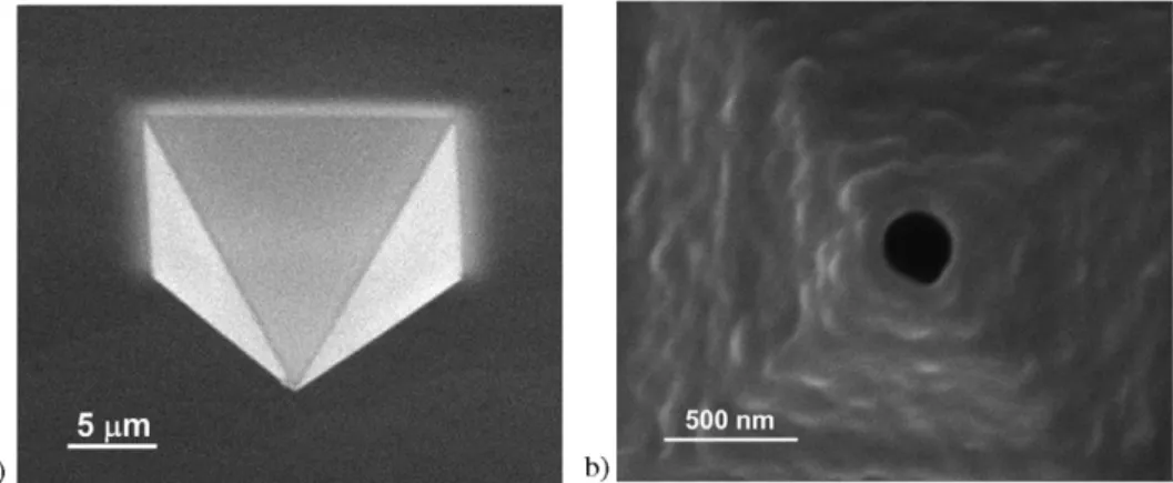
Si cantilever with a hollow SiO2 pyramid tip (pyramid tip see figure 2(a)) is attached to a microscope objective of 8× magnification (not shown). The system uses beam deflection feedback from the cantilever for distance control as it is well known from AFM (atomic force microscopy). The beam deflection laser as well as the near-field excitation laser are focused through the top objective onto the cantilever and into the pyramid tip, respectively. The pyramid shows a nanoscopic opening of approx. 200 nm acting as a near-field aperture for illumination of the sample, see figure 2(b). Illumination wavelengths were chosen from 430 to 610 nm and from 550 to 700 nm using a Fianium supercontinuum free space laser coupled via a monochromator into single mode optical fibers of the specified ranges. The optical signal was collected in far-field transmission through a 40×/0.60 collection objective on the bottom. The SNOM signal was recorded simultaneously with the AFM topography allowing for direct correlations.
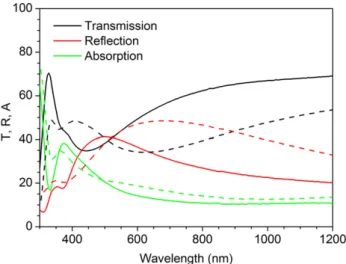
The nanoparticle assemblies were prepared by thermal growth: an 18 nm thin Ag film was evaporated onto a microscope slide and onto a 100 nm thick TCO layer— here a sputtered In2O3:Mo film—on a microscope slide, respectively. The samples were then annealed at 200◦C for 1 h to form nanoparticles. Figure 3shows scanning electron microscopy (SEM) pictures of the nanoparticles on In2O3:Mo which have an ellipsoidal shape of approximate lateral size of 50 nm×75 nm half lengths of the main axis (estimated from the top view in figure 3(a)) and a height of approx. 60 nm (as deduced from the 70◦ side view in figure3(b)). The resonance wavelength of the samples was determined by integrating sphere measurements using a lambda950 UV–vis photospectrometer. Transmission, reflection and absorption are depicted in figure 4 as solid lines for the nanoparticles on glass and as dashed lines for the nanoparticles on In2O3:Mo/glass. The resonance position is characterized by a minimum in transmission resulting from maxima in reflection and absorption. It shifts from 450 to 630 nm with the increase of substrate refractive indexngoing from glass (n=1.5) to In2O3:Mo (n decreases from 2.2 to 1.9 for the wavelength range shown).
Figure 2. SNOM tip: (a) pyramid tip and (b) nanoscopic tip opening for light transmission; typical approx. size 200 nm.
et al
Figure 3. Scanning electron microscopy picture of Ag nanoparticles obtained by thermal growth on In2O3:Mo; (a) top view, (b) 70◦side view.
Figure 4. Transmission, reflection and absorption of Ag nanoparticles deposited on glass (solid lines) and on 100 nm In2O3:Mo on glass (dashed lines).
3. Scanning near-field optical microscopy
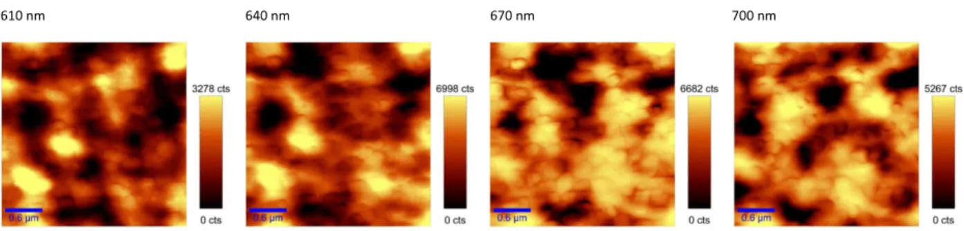
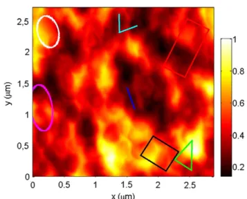
Given the range of illumination and the resonance wave-lengths of the samples as derived from optical measurements, the focus of SNOM investigations was for the sample of Ag nanoparticles on In2O3:Mo/glass in the range from 550 to 700 nm. Figure 5 shows in the left column the topography, in the right one the simultaneously recorded near-field optical image as a series of wavelength. Drift can be seen at a closer look to the topography pictures. It could partially be corrected for by adjusting the scanning area and it is furthermore considered by drawing various shapes to guide the eye to regions of specific interest. These shapes are repeated at the according locations of the optical pictures. The AFM resolution clearly resolves the nanoparticles. The resolution stays good throughout the whole series indicating that there was no major tip change—and related possible change of the opening of the near-field aperture by picking up material. The intensity range of the SNOM pictures is dropping down for the wavelengths of 550 and 700 nm, which are at the margins of
the optical fiber transmission. But the signal is still sufficient to obtain optical resolution.
The shapes in figure 5 are drawing attention to selected individual, conjoint and assembled nanoparticles. The according areas in the optical pictures are marked by various transitions from bright to dark or dark to bright which we will try to find explanations for. Four major points can be mentioned that will influence the measured field intensities. (1) A metal nanoparticle of a given size and shape (and
material) has a defined plasmon resonance frequency. With changing the particle’s size and especially the shape (which in the here considered method of fabrication by thermal growth often goes along with the size) the resonance frequency will shift. The trend is a red-shift with increasing size and elongation [15]. Differently sized and shaped particles will therefore experience their transition through resonance at different wavelengths. (2) The scattering and the absorption cross section of a
plasmonic nanoparticle are several times larger than its geometric cross section [1]. In the case of Ag this is a factor of approx. 5 which means that a circularly assumed area with 2.2 times the particle radius is affected by the particle’s absorption and scattering.
(3) Depending on the particle size, either absorption or scattering will dominate. Generally, smaller particles show a higher parasitic absorption, whereas big particles are the better scatterers. For Ag particles with radii above 40 nm scattering has started to dominate absorption and radii over 60 nm are related to scattering efficiencies above 80% (for spherical particles at air/TCO interface, see [16]). Also scattering is more efficient on the red side of the resonance whereas the absorption is more prominent in the blue.
(4) It is not only the light scattered from the nanoparticles that needs to be considered for interpreting the detected transmission but also the light that passes the sample without interacting with a nanoparticle. The combination of the two processes will lead to an overlay of simply transmitted and of scattered light and will result in Fano resonances [13,14]. In our specific case we can break it
J. Opt.15(2013) 125001 M Schmidet al
Figure 5. Topography and optical signal measured on a sample of Ag nanoparticles on 100 nm In2O3:Mo/glass for various wavelengths from 550 to 700 nm. Selected particles and assemblies are marked to guide the eye to areas of specific interest.
et al
Figure 6. Optical signal measured for a sample of Ag nanoparticles on 100 nm In2O3:Mo/glass for various wavelengths from 610 to 700 nm. The tip was kept at constant height without pushing force.
down to the main fact that there may occur a transition from destructive to constructive interference when passing the resonance. For wavelengths below the resonance the scattered light shows a π phase shift with the incident light and therefore interferes destructively with the simply transmitted light. At longer wavelengths there will be no phase shift of the scattered light and thus constructive interference.
With these general descriptions of plasmonic effects in mind we now exemplarily address three nanoparticle arrangements as visible in figure5.
(i) A single (big) particle dominates (see e.g. the particle marked with a white circle on the top left in the pictures of figure5). In this case mainly the Fano like overlap of scattered and non-scattered light as described under (4) is expected to dominate. Assuming that the amplitudes are balanced—which appears justified for this case of isolated particle—a transition from dark to bright when sweeping from 550 to 700 nm through the resonance can be explained.
(ii) The uncovered surface between particles dominates (see e.g. the black box depicted on the bottom in figure 5). Generally, a high transmission, e.g. a bright signal, is expected from these areas. Yet, when approaching the resonance wavelength, neighboring particles will strongly absorb light and since the absorption cross section of a metal nanoparticle may significantly surpass its geometrical cross section (as outlined in (2)) they also absorb light from uncovered areas. These formerly bright areas therefore turn dark.
(iii) Mainly smaller particles of different shapes and with varying distances come together. For these nanoparticles their different resonance wavelengths have to be considered (see (1)), which may be out of the range investigated in figure 5. Furthermore, either much light is transmitted if they are sparsely scattered or strong interactions may dominate if they are closely packed. The higher parasitic absorption of these smaller nanoparticles compared to bigger ones will lead to a generally darker occurrence in the blue wavelength, whereas the lower reflection due to smaller coverage area will lead to a higher transmission in the red wavelengths (see also (3)).
The red rectangle on the top right in figure 5 gives an example for such an area, see especially the dimers around the bottom right corner.
These three examples illustrate the general behavior of plasmonic metal nanoparticles. The contribution of different effects that are in addition strongly dependent on particle sizes, shapes and density complicate a coherent explanation of the observed optical signals. The above given trends were however also found for the sample nanoparticles on glass, yet in the measurement range 430–610 nm since the resonance wavelength lies at 450 nm here. The cases (i)–(iii) may be partially identified although the resonance is very close to the lower end of the wavelength range. Multiple transitions still occurring above resonance are related to a range of resonance positions reaching into higher wavelengths. Also for the sample nanoparticles on In2O3:Mo/glass still changes in optical contrast are observed in the range of 430–610 nm. In this case resonances of smaller particles as well as higher order modes contribute. (No image series shown.) Strong changes in the SNOM contrast with varying the excitation wavelength across the resonances was studied by [17] on colloidal clusters and similar changes from hot to cold spots found.
In several optical pictures the broad combined scattering distribution from the nanoparticle assemblies is visible together with resolution of transmission on the size of individual particle features. By performing constant height measurements it was ruled out that these particle features are a result of cross talk between topography and optical signal. Figure6 shows a series of optical pictures recorded without any pushing force on the cantilever and a simultaneous topography of zero (resulting unicolor topography pictures not shown). The measured variations of scattering intensity are fully reproducible when returning to the initial wavelength after a sweep again. The optical pictures clearly show particle structures. Yet, the pictures also clearly show that there is never just the interaction between the light and one nanoparticle, but the nanoparticles experience strong interactions in their scattering properties resulting in a ‘collective effect’ of particle scattering.
A collective scattering effect is to be expected considering the high density of the nanoparticles and their large scattering cross sections. The emerging collective
J. Opt.15(2013) 125001 M Schmidet al
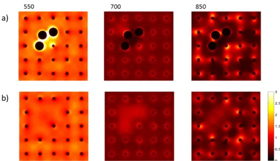
Figure 7. Array of 125 nm diameter, 225 nm pitch Ag hemispheres on In2O3:Mo/glass with a distortion of regularity and (a) increased, (b) decreased particle size in the upper left of the picture. FDTD calculations of the electric field distribution in a plane 60 nm above the substrate surface are shown for the three different wavelengths 550, 700 and 850 nm. Thez-scale is in V2m−2.
Figure 8. Transmission, reflection and absorption extracted from FDTD simulations of an array of 125 nm diameter, 225 nm pitch Ag hemispheres on In2O3:Mo/glass with a distortion of regularity and increased (‘distortion big’) or decreased (‘distortion small’) particle size (see also figure7).
behavior was e.g. also investigated by Huang et al who gradually reduced the particle distance and observed a much more blurred optical response [11] or by Maier et al who investigated coupling in linear particle chains [18]. Next we will make the attempt to understand collective behavior better using numerical simulations related to our structures.
4. FDTD simulations
We study theoretically the scattering behavior of nanoparticle assemblies using finite-difference time domain (FDTD) simulations with the program Lumerical. As a simple reference example we firstly investigate regular nanoparticle arrays including small distortions to find out about their impact. Ag nanostructures on In2O3:Mo/glass were modeled
based on the Ag dielectric data according to Palik [19] and values for In2O3:Mo derived from transmission and reflection measurements. The structures were in the simple case illuminated with a plane wave source and the electric field was monitored on top of the nanoparticles, since this is the focal plane of the recording transmission objective. It has to be added that in our case the substrate (i.e. In2O3:Mo/glass) has the higher refractive index (than air) so that most of the scattered light is directed to transmission. In the pictures, both s- and p-polarization were taken into account and averaged. In following steps further realistic details of the SNOM measurements on random structures need to be considered. These are the illumination through an aperture tip, the far-field recording through a microscope objective with aperture <1 and the specific random nanoparticle distribution. We will discuss these points in order to highlight the various factors of influence to be taken into account when attempting to precisely simulate the experimental setup.
Initially, a regular particle array featuring small distortions was simulated. The regular array consists of Ag hemispheres with a diameter of 125 nm and a pitch of 225 nm. Within the simulated regular array small distortions were introduced in order to investigate the influence of different particle sizes and deviations from the regular arrangement. One particle was slightly shifted from its regular position and this particle as well as the two it was approaching were either increased (‘distortion big’) or decreased (‘distortion small’) for 30 nm in radius, see figures 7(a) and (b), respectively. Hemispheres were chosen in this basic arrangement since the higher contact area to the substrate shifts the resonance position to a wavelength better comparable to the one of elliptical particles, although in this specific case of array the resonance wavelength is with approx. 700 nm a little higher than in our experimental data (630 nm). The resonance is derived from figure 8 where transmission, reflection and 6
et al
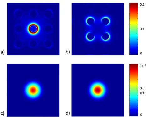
Figure 9. FDTD simulation of a (100 nm) Al/SiO2SNOM tip over an array of 125 nm diameter, 225 nm pitch Ag hemispheres on In2O3:Mo/glass with (a) the tip directly on top of a particle and (b) the tip in the middle between four particles. The electric field was recorded forλ=700 nm (e.g. at the resonance) at a horizontal monitor at 35 nm above the In2O3:Mo surface. Thez-scale is in V2m−2. (c) and (d) show the far-field projections into an NA = 0.6 objective for the respective cases of (a) and (b).
absorption of the nanoparticles are plotted. At the resonance wavelength the absorption and the reflection are maximum whereas the transmission experiences a minimum. This occurs at 700 nm and much less pronounced at 375 nm. At the main resonance the absorption of the array with distortions by big particles is comparable to the array with distortions by small particles. The reflection however is higher when considering distortions by big particles resulting in a smaller transmission. This observation of reduced transmission thus is a result of higher coverage by the nanoparticles and related scattering not of higher absorption (the absorption to scattering ratio is still bigger for the small particles).
The electrical field distributions on top of the nanopar-ticles are shown in figure7 for the resonance wavelength of 700 nm flanked by 550 and 850 nm. For the regular sized particles the area in between them appears darkest around the resonance which reflects the minimum transmission. At wavelengths below and above the resonance where the transmission increases they become brighter. Therefore the electric field distributions can be considered as representatives for the observed transmission images as they are recorded in the SNOM experiments. Considering now in particular the distortions we see that especially the area in between these particles of different sizes undergoes the most distinct changes. Around the distortion by big particles (figure7(a)), the dark appearance at 700 nm is even more pronounced. This extends up to approx. 800 nm (without picture) resulting from a red-shift of the resonance for the bigger particles. At 550 and 850 nm—off resonance—however, strong electric fields emerge between the particles. For the case of the distortion by small particles (figure7(b)), the transition of dark to bright occurs as well but is blue-shifted due to an expected lower
resonance wavelength of these small particles. Compared to the surrounding the area around the small particles becomes brighter from 550 to 700 nm and still at 850 nm. Taking into account that a random assembly of nanoparticles includes both, smaller and bigger particles, it becomes comprehensible, that a picture recorded for this situation will include multiple aspects of theoretically ideal structures together with various resonance frequencies and is therefore much more challenging in interpretation. But what we can learn is that with deviations from regular arrangement and variations in particles size, strong fields between the particles may emerge and become dominant. This finding is in agreement with literature where also strong localizations of electric fields were observed between closely spaced nanoparticles [10,12,20].
The simple reference example gave us first ideas about electric field distributions in irregular nanoparticle arrays. In order to describe the realistic situation of measuring random nanoparticles assemblies with a SNOM several further factors need to be considered: in this case the illumination takes place through an aperture tip which is scanning across the sample. Furthermore, the measurement of the far-field transmission through a microscope objective needs to be taken into account by restricting the simulated transmission intensity with the numerical aperture of the objective. Finally, of course also the realistic topology has to be considered, which may be achieved by importing the measured AFM data into the simulation. In the following we will discuss these various points and give implications for a detailed simulation of realistic nanoparticle assemblies.
An exemplary simulation for a (100 nm) Al/SiO2SNOM tip (opening 200 nm) over a Ag nanoparticle array (regular
J. Opt.15(2013) 125001 M Schmidet al
area from figure7) on 100 nm In2O3:Mo/glass is shown in figure9. The resonance wavelength of 700 nm was chosen and the horizontal monitor put at half height of the particles, i.e. 35 nm from the In2O3:Mo interface, to better see the ring-like appearance around the nanoparticles. Comparing the position of the tip directly on top of a nanoparticle (figure9(a)) to a position in the middle between four particles (figure9(b)) we see that the general occurrence is very similar, but asymmetries appear that are related to the presence of the tip. Considering the four different positions a tip could have around one nanoparticle—always being in the center of four particles—and notionally averaging over these four pictures, we would return to a field distribution similar to the one where the tip is on top of the particle. This shows us the difference of assuming a plane wave versus a tip source—namely the stronger asymmetric appearance of the shapes, yet no profound change in the overall electric field distribution. The additional asymmetries in the measurements will indeed be better described by considering the tip. Furthermore, the far-field projections into a microscope objective with NA = 0.6 are shown in figures9(c) and (d) for the respective cases (a) and (b). It is furthermore interesting to note that the maximum intensity collected through this NA = 0.6 aperture is approx. 10 times smaller than it would be through an NA = 1 objective (pictures not shown).
For finally simulating the realistic case of SNOM measurements on random nanoparticle assemblies, also the realistic topology, in particular the specific arrangement of the nanoparticles in the experimental configuration, would need to be considered, which may be feasible using the AFM-measured topography in the simulation. This simulation structure closely representing the particular experimental setting, then would need to be combined with a representation of the illumination tip as outlined before. For each position of the tip for its scan across the sample a simulation and recording of the far-field projected into the microscope objective would need to be taken. The execution, however, requires enormous computation efforts and times and therefore cannot be presented here. A comprehensive theoretical understanding of the working mechanisms of nanoparticle scattering therefore remains challenging. Yet, scanning near-field optical microscopy experiments can provide important information about the local distribution of electric fields which is important for evaluating possible absorption enhancement in solar cells.
5. Impact
Our aim of investigating optical properties of dense random arrays of Ag nanoparticles on the nanoscale was to find out about the local electric field distribution and the impact on the performance of a solar cell with these nanostructures integrated. We deliberately choose these dense random structures since they are widely considered to promote absorption enhancement in thin-film solar cells. In our investigations we focus on Ag nanostructures on top of a thin TCO layer on glass. In this configuration the nanoparticles may be integrated in the front or the back contact of a solar
Figure 10. Expected optical generation rate for a solar cell with integrated random assemblies of nanoparticles. The measured optical data as shown in figure5were weighted by the AM1.5G spectrum as well as by the measured transmission through the sample for the different wavelength intervals given.
cell. For the case of back contact, we of course would need to consider that the then adjacent absorber material with an even higher refractive index than the TCO would lead to a red-shift of the resonance. Yet, since it is the higher n material, the scattered light would be preferentially scattered towards it [1] and thus again show its impact in the absorber layer. When the nanostructures were integrated in the front contact, the resonance remains unchanged and the scattered light will be directed towards the absorber in the transmission direction which corresponds to the situation represented in our experiments. Assuming a directly adjacent absorber layer we then can investigate the influence of the observed local electric field distributions on the absorption and resulting performance of the solar cell. As shown in [21], the near-field enhancement contributes to additional absorption that can be measured in the solar cell characteristics.
In order to quantify the impact of locally enhanced electric fields on the solar cell performance we calculate the expected optical generation rate as follows. The measured optical signals shown in figure 5 were firstly normalized. They were then weighted with the independently measured transmission value as depicted in figure 4and finally folded with the AM1.5G solar spectrum for each portion of the solar spectrum. This gives us the local light intensity which may contribute to photocurrent generation (of course still the band gap of the absorber needs to be considered for estimations of maximum local short circuit current density of the solar cell). The result is shown in figure10 and the features marked in figure 5 are repeated to show the influence of the different particle arrangements. The strong variations in the intensity profile of figure 10reveal that the highly non-uniformity of the electric field distribution translates to the expected optical generation rate. Thinking about the resulting performance of a solar cell, these non-uniformities can have a negative influence on the overall device performance [22]. For a device 8
et al
without local scatterers a homogeneous light distribution and thus optical generation rate would be expected which is beneficial for a uniform current generation but which cannot make profit of enhanced fields. This is a trade-off for which to solve detailed investigation of the electric field distributions around nanoparticle assemblies in high local resolution are of great importance. They can help to estimate the impact on possible photocurrent enhancement in combination with solar cells. Near-field optical microscopy which reveals these local electric fields thus constitutes a useful approach to optimize the nanostructures for efficient absorption enhancement.
6. Conclusions
In this paper we investigated the optical properties of random silver nanoparticle assemblies with a resolution in the range of 100 nm. The SNOM pictures show that despite individual particle features can be identified the particles appear to exhibit a collective scattering behavior. This has a significant impact on the local generation rates of a solar cell including random arrangements of nanoparticles. FDTD simulations of particle arrays with distortions proof that variations in particle size and distance lead to strong variations of electric fields in the vicinity of the particles. A comprehensive simulation of near-field optical measurements on random nanoparticle would need to consider the (e.g. AFM-)measured topology, the illumination through an aperture tip and the projection into a microscope objective and thus require enormous computing power. Yet, we showed that with our initial approach we are able to provide first insight to the scattering behavior and identified the impact of further parameters like tip and collection objective aperture. The consideration of local scattering properties of nanoparticles for the integration in thin-film solar cells is expected to be highly advisory to optimize geometries.
Acknowledgments
We thank A Leenher, R Palla and D Turner-Evans for technical support with the SNOM and scientific exchange. V Brar and S Kim are acknowledged for providing FIB and SEM on the tips, respectively, M Jang for computer support and the MMRC (Caltech) for access to the SNOM. M Schmid also thanks M Kirsch for In2O3:Mo sputtering and R Bartmann for discussion. The work of J Grandidier and
H A Atwater was supported by the Department of Energy ‘Light-Material Interactions in Energy Conversion’ Energy Frontier Research Center under Grant DE-SC0001293. M Schmid acknowledges support from the Initiative and Networking fund of the Helmholtz Association for the Young Investigator Group VH-NG-928.
References
[1] Catchpole K R and Polman A 2008Opt. Express1621793
[2] Atwater H and Polman A 2010Nature Mater.9205
[3] Pillai S, Catchpole K R, Trupke T and Green M A 2007
J. Appl. Phys.101093105
[4] Moulin E, Sukmanowski J, Schulte M, Gordijn A, Royer F and Stiebig H 2008Thin Solid Films5166813
[5] Tan H, Santbergen R, Smets A H M and Zeman M 2012Nano Lett.124070
[6] D¨urig U, Pohl D W and Rohner F 1986J. Appl. Phys.593318
[7] Klar T, Perner M, Grosse S, von Plessen G, Spirkl W and Feldmann J 1998Phys. Rev. Lett.804249
[8] Lereu A L, Sanchez-Mosteiro G, Ghenuche P, Quidant R and Van Hulst N F 2007J. Microsc.229254
[9] Chang Y-C, Chen H-W and Chang S-H 2008IEEE J. Sel. Top. Quantum Electron.141536
[10] Aigouy L, Prieto P, Vitrey A, Anguita J, Cebollada A, Gonz´alez M U, Garc´ıa-Mart´ın A, Lab´eguerie-Eg´ea J and Mortier M 2011J. Appl. Phys.110044308
[11] Huang C-H, Lin H-Y, Chang C-H and Chui H-C 2009Proc. SPIE7224722411
[12] Danckwerts M and Novotny L 2007Phys. Rev. Lett. 98026104
[13] Prikulis J, Xu H, Gunnarsson L, K¨all M and Olin H 2002
J. Appl. Phys.926211
[14] Luk’yanchuk B, Zheludev N I, Maier S A, Halas N J, Nordlander P, Giessen H and Chong C T 2010Nature Mater.9707
[15] Maier S A and Atwater H A 2005J. Appl. Phys.98011101
[16] Schmid M, Klenk R, Lux-Steiner M C, Topic M and Krc J 2011Nanotechnology22025204
[17] Markel V A, Shalaev V M, Zhang P, Huynh W, Tay L, Haslett T L and Moskovits M 1999Phys. Rev.B5910903
[18] Maier S A, Kik P G, Brongersma M L and Atwater H A 2001
Proc. SPIE445622
[19] Palik E D 1985Handbook of Optical Constants of Solids
(Boston, MA: Academic)
[20] Wang X, Gogol P, Cambril E and Palpant B 2012J. Phys. Chem.C11624741
[21] Grandidier J, Weitekamp R A, Deceglie M G, Callahan D M, Battaglia C, Bukowsky C R, Ballif C, Grubbs R H and Atwater H A 2013Phys. Status Solidia210255
[22] Sze S M 1981Physics of Semiconductor Devices2nd edn (New York: Wiley)