e-ISSN: 2278-067X, p-ISSN: 2278-800X, www.ijerd.com
Volume 10, Issue 10 (October 2014), PP.70-74
Testing and Relocating of Memory with Address
Programmability
Kosuru.Maruthi
1, Tadi.Venkateswara Reddy,
2C.R.S.Hanuman
31(M.Tech Student in VLSI & Embedded Systems, S.I.T.E, Tadepalligudem, India) 2
(Assistant Professor , ECE Department, S.I.T.E, Tadepalligudem, India )
3(Associate Professor, ECE Department, S.I.T.E, Tadepalligudem, India)
Abstract:-
Most of the System-on-Chip (SoC)‟s area is covered by embedded memories. As these memories are very tightly integrated, consists majority of defects in SoC. Detection of such a complex and diverse faults during fabrication is not possible. Hence leads to failure of soc in field. Usage of test algorithms may increase the coverage of complex faults, but unexpected failures can‟t be covered by these algorithm. Providing possibility of choosing testing algorithms before using in SoC is very important. Programmable BIST approaches, allowing selecting after fabrication a large variety of memory tests, are therefore desirable, but may lead on unacceptable area cost. BIST approaches enabling test algorithm programmability and data background programmability at low area cost have been presented in the past. However, no proposals exist for programming the address sequence used by the test algorithm. In this paper, we extend programmable BIST to complete programmability. This new feature is implemented at low cost by using the memory under test itself to store the desired address sequence and some compact circuitry that enables using this sequence for testing the memory.Keywords:-
Built In Self Test (BIST), Memory BIST (MBIST), Memory test algorithms, System-on-Chip (SoC).I.
INTRODUCTION
Nowadays, the area occupied by embedded memories in System-on-Chip (SoC) is about 90%, and expected to rise up to 94% by 2015. As those memories are very tightly integrated with large number of transistors causes 90% of overall faults in system on chips Thus, they concentrate the large majority of defects. In addition, with aggressive nanometer scaling, defect types are becoming more complex and diverse and may escape detection during fabrication test. If they are not treated adequately, the above trends will increase defect level, affect circuit quality dramatically and impact reliability, as undetected fabrication faults will be manifested as field failures. To cope with, the ability to guaranty a high quality test should be integrated in memory BIST, which is the mainstream test technology for embedded memories. Memory BIST generators can integrate a limited set of test algorithms [1],[2],[3]. Thus, only the test algorithms selected during the design phase can be used after fabrication. However, fixing the memory test algorithms during the design phase is not a good strategy as unexpected failures may be discovered after production. Also, integrating pre-emotively a large number of test algorithms in the BIST generator will result in large area cost. Thus, programmable memory BIST enabling selecting the memory, test stimuli in silicon and testing the memory for a wide variety of faults is becoming mandatory. This flexibility has to be achieved at low area cost, to make the approach attractive for real products. Also, the flexibility offered by programmable BIST is highly important for thorough screening inspection, failure analysis of customer returns, debug of a new fabrication process or a new memory design, and production ramp-up, since the most challenging issue in these processes is to detect and/or diagnose unexpected failures.
programmability of the address sequence used concerns the large amount of data that have to be programmed (here the complete memory address space) and the associated high hardware cost. We resolve this problem by adapting the transparent BIST scheme [10],[11] in a way enabling storing the address sequence in the memory under test and using it for testing the memory.
II.
FAULT MODELS, TEST ALGORITHMS
A fault model is a systematic and precise representation of physical faults in a form suitable for simulation and test generation [11]. Applying the reduced functional model, SRAM faults can be classified as follows: 1. Address Fault (AF), 2. Address Decoder Open Faults (ADOF), 3. Coupling Faults (CF), 3a. Inversion Coupling Faults (CFin), 3b. Idempotent Coupling Faults (CFid), 3c. State Coupling Faults (CFst), 4. Bridge Coupling Faults (BF) 5. Data Retention Faults (DRF) 6. Stuck-at Faults (SAF), 7. Stuck Open Faults (SOF), 8. Transition Faults (TF)
An efficient memory test should provide the best fault coverage in shortest time [13].March tests have the advantage of shortest test time with good fault coverage. There are many March tests such as March C, March C-, March C+, March 3 and so on. Table .1 compares the test length, complexity and fault coverage of them. „n‟ stands for the capacity of memory.
Algorithms
Test length Complexity
Fault coverage
March C-
10n
O(n)
AF, SAF, SOF,CF
March SS
22n
O(n)
AF, SAF, SOF, CF
M0M1
4n
O(n)
SAF, SOF
March LR with BDS
23n
O(n)
AF, SAF, SOF, CF
Table: 1 Comparison of different March tests
As shown in TABLE 1, March C- has better fault coverage than March C and shorter test time than March C and March C+. So March C- has been chosen as BIST algorithm in this Paper.
III.
BISR STRATEGY WITH REDUNDANCY ARCHITECTURE:
SRAM BISR strategy is flexible. The SRAM users can decide whether to use it by setting a signal. So the redundancy of the SRAM is designed to be selectable. In another word, some normal words in SRAM can be selected as redundancy if the SRAM needs to repair itself. We call these words Normal-Redundant words to distinguish them from the real normal ones.
Figure: 1 Architecture of redundancy in SRAM
IV.
PROGRAMMABLE MEMORY BIST
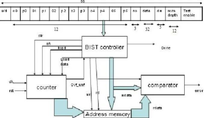
Work on most of programmable memory BIST approaches concerns the programmability of the memory test algorithm [4],[6],[8]. The programmable memory BIST proposed in [7] has several advantages. It enables programming both test algorithms and test data. It implements test algorithm programmability at low cost, by extracting the different levels of hierarchy of the test algorithm and associating a hardware bloc to each of them, resulting on low cost hardware. It enables low-cost implementation of full-data Programmability by adapting the transparent memory test approach [10-16] in a manner that uses the memory under test for programming the test data. As stated in the introduction, the aim of this paper is to extent the above programmable BIST scheme to enable programming the address sequence, thus enabling programmability of all components of memory test: test algorithm; test data; address sequence. The architecture for programming march test algorithms proposed in [7] (and implemented and evaluated in [8]). This architecture uses an Instruction Register specifying the current match test sequence by means of several fields indicating: the number of operations (NO) performed by the current march sequence; the order Up or Down (U/D) in which the address counter is used; the address mode like fast-X, fast-Y, fast-D (@mode); several operation fields (O1, O2, Om-1), each determining one of the operations used by the march sequence (usually read and write, but other operations like read-modify-write, no operation, etc are also supported if necessary); the value of the memory word (DATA) to be used during the march sequence (fewer bits that the actual memory word can be used and expended by the BIST circuitry to create the full word); one data polarity bit for each operation field (P1, P2, Pm-1), specifying if the corresponding operation uses the data word in its direct or complemented form; a wait bit (W) forcing all the operations of the march sequence to the non-operation (idle) mode, in order to implement a retention test; a bit (TE) set to 1 only at the last instruction of the test algorithm to indicate that the test finishes at the end of the current march sequence.
Figure 2: Proposed Architecture for Programming March C- Algorithm
Each field of the Instruction Register is interpreted by a specific block of the BIST architecture shown in Fig: 2. They enable a very compact implementation resulting on low-cost programmable BIST allowing selecting in silicon any march test algorithm at will, provided that its longest march sequence can be supported by the number of Operation fields and Polarity bits of the Instruction Register, selected during the design phase. As this size only impacts the size of the Instruction Register (linearly), the size of the Control MUX (linearly) and the size of the Cycles Counter (logarithmically), selecting a large number of operations will slightly affect the BIST area and can be done comfortably, to cover any march test algorithm of realistic length. March test algorithms are powerful and can be designed to test a wide range of static and dynamic memory fault models.
V.
SELF REPAIRING MECHANISM WITH BISR:
The architecture of the proposed BISR strategy is shown in Fig:3
.
It consists of three parts: PBIST module, BIAA module and MUX module. We call the SRAM with BISR a system. The BIST module uses March C- to test the addresses of the normal words in SRAM. It detects SRAM failures with a comparator that compares actual memory data with expected data.Figure: 3 Proposed BISR Architecture.
If there is a failure (compare_Q = 1), the current address is considered as a faulty address. The BIAA module can store faulty addresses in a memory named Fault_A_Mem. There is a counter in BIAA that counts the number of faulty addresses. When BISR is used (bisr_h = 1), the faulty addresses can be replaced with redundant addresses to repair the SRAM. The inputs of SRAM in different operation modes are controlled by the MUX module. In test mode (bist_h=1), the inputs of SRAM are generated in BISR while they are equal to system inputs in access mode(bist_h= 0).
VI.
TRANSPARENT BIST APPROACH
We present a scheme enabling programming the address sequence used by March test algorithms without any limitations (i.e. any address sequence can be programmed in silicon). Enabling programming at will the full address space would require an auxiliary memory of large capacity for storing any memory address sequence selected after fabrication. We observe that the number of addresses of the auxiliary memory is the same as the number of addresses of the memory under test. Based to this observation, we eliminate the auxiliary memory and instead we use the memory under test to store the desired address sequence. We store it in a manner that allows producing the desired address sequence during the March tests. We adopt the transparent BIST approach in order to preserve the stored address sequence during testing.
VII.
SIMULATION RESULT AND CONCLUSION:
As these benefits are obtained at low area cost, the proposed memory BIST becomes highly attractive not only for test chips dedicated to new memory and/or process debug but also for integrating it into final products. The proposed BIA (built in analyzer) was simulated with ModelSim PE student version using Verilog is shown in Fig:4.
REFERENCES
[1]. Semiconductor Industry Association, “International technology roadmap for semiconductors (ITRS), 2003 edition,” Hsinchu, Taiwan, Dec.2003.
[2]. C. Stapper, A. Mclaren, and M. Dreckman, “Yield model for Productivity Optimization of VLSI Memory Chips with redundancy and Partially good Product,” IBM Journal of Research and Development, Vol. 24, No. 3, pp. 398-409, May 1980.
[3]. W. K. Huang, Y. H. shen, and F. lombrardi, “New approaches for repairs of memories with redundancy by row/column deletion for yield enhancement,” IEEE Transactions on Computer-Aided Design, vol. 9, No. 3, pp. 323-328, Mar. 1990.
[4]. P. Mazumder and Y. S. Jih, “A new built-in self-repair approach to VLSI memory yield enhancement by using neuraltype circuits,” IEEE transactions on Computer Aided Design, vol. 12, No. 1, Jan, 1993. [5]. H. C. Kim, D. S. Yi, J. Y. Park, and C. H. Cho, “A BISR (built-in self repair) circuit for embedded memory with multiple redundancies,” VLSI and CAD 6th International Conference, pp. 602-605, Oct. 1999.
[6]. Shyue-Kung Lu, Chun-Lin Yang, and Han-Wen Lin, “Efficient BISR Techniques for Word-Oriented Embedded Memories with Hierarchical Redundancy,” IEEE ICIS-COMSAR, pp. 355-360, 2006. [7]. C. Stroud, A Designer‟s Guide to Built-In Self-Test, Kluwer Academic Publishers, 2002.
[8]. Karunaratne. M and Oomann. B, “Yield gain with memory BISR-a case study,” IEEE MWSCAS, pp. 699-702, 2009.
[9]. I. Kang, W. Jeong, and S. Kang, “ High-efficiency memory BISR with two serial RA stages using spare memories,” IET Electron. Lett., vol. 44,no. 8, pp. 515-517, Apr. 2008.
[10]. Heon-cheol Kim, Dong-soon Yi, Jin-young Park, and Chang-hyun Cho, “A BISR (Built-In Self-Repair) circuit for embedded memory with multiple redundancies,” in Proc. Int. Conf. VLSI CAD, Oct. 1999, pp. 602-605.
[11]. M. Sachdev, V. Zieren, and P. Janssen, “Defect detection with transient current testing and its potential for deep submicron CMOS ICs,” IEEE International Test Conference, pp.204-213, Oct. 1998.
[12]. Mentor Graohics, MBIST Architect Process Guide, Software Version 8.2009_3, Aug 2009, pp. 113-116.